e-ISSN: 2278-7461, p-ISSN: 2319-6491
Volume 6, Issue 2 (Feb 2017) PP: 58-66
A Comparative Study of Electrical Properties of Si and ZnO
Gate-all-around Nanowire FET
Syed Zahin Reza
1, Md. Shahrul Islam
2, Fahad Al Mamun
31,2,3
Department of Electrical and Electronic Engineering, Islamic University of Technology, Board Bazar, Gazipur- 1704, Bangladesh
Abstract:-
A comparative study of various electrical properties of n-channel Si And ZnO Gate-all-around (GAA) nanowire Field-Effect Transistors has been assessed and presented. The simulation results shown here are found on the basis of self-consistent solution of energy balance equation. The temperature, channel diameter and gate length dependence of various electrical parameters like subthreshold swing (SS), threshold voltage and transconductance have been simulated. ZnO nanowire FET showed better threshold voltage but poor subthreshold swing and transconductance with respect to Si nanowire FET.Keywords: GAA, Si, ZnO, Nanowire FET, SS, Threshold voltage, Transconductance
I.
INTRODUCTION
In modern electronic circuits, transistors have been implemented as basic modeling elements. For the past few decades, MOS devices have been developed at a dynamic pace [1]. From Moore’s law, dimensions of transistors have been reduced to nanoscale. Although varying of dimensions affects information processing system of transistors, it might cause few technical problems [2]. Gate-all-around (GAA) FET is advantageous over FinFET and silicon-on-insulator (SOI) technology as it overcomes the problem of mobility loss due to channel width variations. GAA FET is a nanowire structure where the gate surrounds all the four sides of the channel. This structure enables the transistor to obtain good gate control over the channel which is very much integral for building next generation nanowire transistors. The knowledge of working methods of solid state devices is indispensable for device physics. Simulation is becoming very much important for understanding different process parameters of NWTs. Simulation tools can assist experimental work to modify the FETs [3], minimize their cost, point out their pros and cons, and demonstrate their scalability down to the nanometer range [4-5].
II.
NEED
AND
SCOPE
OF
PRESENT
STUDY
ZnO is touted as one of the most pre-eminent II-VI semiconductors that have been investigated since the early 1930s [6-7]. ZnO is a direct bandgap material having a bandgap of about 3.4eV [8]. It crystallizes in the hexagonal wurtzite type structure [8]. ZnO has become an alluring choice for transparent conductors and FET as it has large bandgap and possibility of introducing n type dopants is also there [9]. The bandgap modulation over wide range by alloying cadmium and magnesium has been demonstrated for UV-optoelectronics [6]. Nanoparticles and nanowires of ZnO have been implemented as electron transport layer in dye-sensitized solar cell [10-11]. Development of 1-D ZnO nanostructures as biosensors is in the initial but potential stage [12-17]. Various enzymes have been deactivated in order to realize highly selective bioassays [18-20]. Surface modification of ZnO nanowires with biotin for streptavidin detection has been reported recently [21]. For uric acid detection, Enzyme coated ZnO nanowire FET have been used [22]. In literature, further ZnO nanowire use for DNA sensory applications can be observed [23]. There have been several studiesfocusing on the development of Si-NWsensors during the last decade due to availability and ease of fabrication [24-26]. Si-NWs are CMOS compatible [27]. But ZnO-Si-NWs are not CMOS compatible but it works quite well under ambient conditions and oxygen rich environment [28-30]. The industry has reached the saturation limit and the need for better and efficient material for nanowire FET has increased greatly with the span of time. Thus ZnO can become a good alternative. In this paper, a comparative simulation based study of different parameters has been provided considering the importance and increasing demand of Si and ZnO nanowire transistors in different applications.
III.
DEVICE
CONFIGURATION
AND
SIMULATION
METHODOLOGY
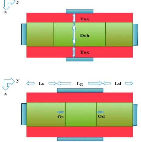
source and drain lengths were both chosen 100nm and the gate length has been varied in the range of 500 nm to 800 nm, channel diameter from 20 nm to 60 nm. The oxide thickness has been taken 10 nm and kept constant throughout the simulation studies. The drain and source doping has been kept fixed at 2 1024 cm-3 and channel doping was 8 1016 cm-3. The gate bias was varied from -1.5 V to 2 V whereas drain bias has been kept at 0.8V. Oxide overlap has not been considered.
Fig. 1. Two Dimensional structure of Gate-all-around Nanowire FET device for geometry- x and for geometry- y [31]
A simulation tool named MuGFET was used to observe various effects of the nanowire parameters like temperature, gate length and channel diameter on NWT Id–Vg characteristics. The MuGFET software was
designed and developed at Purdue University. MuGFET is a software for simulating different electrical properties for nanoscale multi-gate FET structures [31]. FromMuGFET, PADRE simulator was used which was developed at Bell Laboratories. PADRE is basically a device oriented simulator for 2D/3D device with arbitrary geometry. It delivers many plots which come useful for better understanding of device operation. MuGFET provides self-consistent solutions to the Poisson and drift-diffusion equations for the calculation of the characteristics of NWTs [32].
TABLE I. List of various properties of Si and ZnO channel materials at 300 K undertaken for simulation study
S. No. Properties Si ZnO
1 Energy band-gap (eV) 1.12 3.37
2 Dielectric constant 11.7 8.49
3 Electron affinity (V) 4.05 4.35
4 Electron effective mass 0.2mo 0.26
5 Light Hole effective mass 0.16mo 0.59mo
6 Heavy Hole Effective mass 0.49mo 0.59mo
5 Density of states
effective mass
Electrons 1.18mo 0.29mo
Holes 0.81mo 1.21mo
6 Electron mobility (cm2/V-s) 1450 300
7 Hole mobility (cm2/V-s) 500 5
8 Saturation
Velocity (cm/s)
Electrons 1.0 107 2.24 x 10⁷
IV.
SIMULATIONS
AND
RESULTS
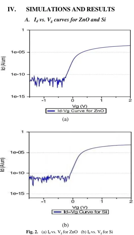
A. Id vs. Vg curves for ZnO and Si
(a)
(b)
Fig. 2. (a) Id vs. Vg for ZnO (b) Id vs. Vg for Si
In fig. 2(a), it is shown that the normalized Id-Vg graph for ZnO with moderately doped channel at 300K was simulated. It is observed from the graph that the on/off current ratio is about 106. The threshold voltage and subthreshold swing were found to be 0.394V and 113.891 mV/decade respectively. The simulation results were fairly in consonance with the experimental data for ZnO nanowire FET [33]. In fig. 2(b), the Id-Vg graph for Si with moderately doped channel at 300K was shown. The gate length was chosen 800 nm and diameter was fixed at 60 nm for both ZnO and Si.
B. Subthreshold Swing vs. Temperature, Channel Diameter and Gate Length
(b)
(c)
Fig. 3. (a) Subthreshold Swing vs. Temperature (b) Subthreshold Swing vs. Channel Diameter (c) Subthreshold Swing vs. Gate Length
In fig. 3(a), it has been observed that subthreshold swing increased with temperature as expected. At room temperature ZnO showed much worse subthreshold swing compared to Si. In fig. 3(b), subthreshold swing vs. channel diameter was plotted. The subthreshold swing increased for both Si and ZnO, ZnO showing the higher subthreshold swing. Similarly, in fig. 3(c), subthreshold swing vs. gate length was plotted. The subthreshold swing of Si was quite stable at all gate length whereas subthreshold swing of ZnO decreased steeply. At long gate length, ZnO and Si showed similar subthreshold swing.
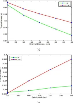
C. Threshold Voltage vs. Temperature, Channel Diameter and Gate Length
(b)
(c)
Fig. 4. (a) Threshold voltage vs. Temperature (b) Threshold voltage vs. Channel diameter (c) Threshold voltage vs. Gate length
The threshold voltage is a fundamental technological parameter that should be maintained properly for a nanowire device.In fig. 4 (a), by varying temperature from 270K to 310K, the decrease observed in threshold voltage in ZnO was found less steep than Si. ZnO provided higher threshold voltage than Si. In fig. 4 (b), this is also true for channel diameter while the diameter was varied from 20 nm to 60 nm. In fig. 4 (c), with the increase of gate length, threshold voltages increases. As the distance between the drain and source decreases, potential becomes more prone to drain electric field encroachment leading to an earlier threshold point of gate bias. Although the initial value for ZnO was lower than Si, the value of threshold voltage of ZnO increased very steeply with the increase of gate length. In all cases, Si offered worse threshold voltages. Lowering this threshold tends to result in the channel never being fully switched off – it’s always leaking some current. From this perspective ZnO would be preferable for most logic application. However for low power device power efficiency is obtained by lowering threshold where Si would be useful.
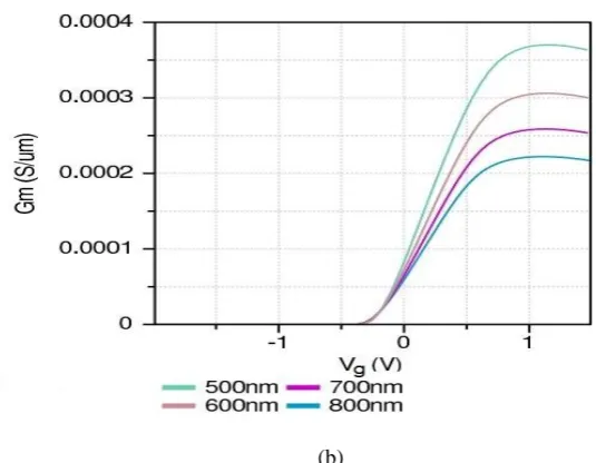
D. Transconductance vs. Temperature, Channel Diameter and Gate Length
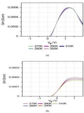
Transconductance, gm, is a measure of the sensitivity of drain current to changes in gate-source bias.
(a)
(b)
Fig. 5. (a) Transconductance vs. Temperature for Si (b) Transconductance vs. Temperature for ZnO
In fig. 5(a), by varying temperature from 270 to 310K, it is observed that the highest transconductance
for Si was achieved near about 1.2V. The transconductance for Si nanowire was quite stable. In fig. 5 (b), it is shown that for ZnO, highest transconductance was achieved near about 0.8V.
(b)
Fig. 6. (a) Transconductance vs. Channel Diameter for Si (b) Transconductance vs. Channel Diameter for ZnO
In fig. 6 (a), it is shown that for Si, with the increase in channel diameter, the highest transconductance was increased and shifted to the right. In fig. 6 (b), it is shown that for ZnO, as the channel diameter increased, the highest transconductance decreased.
(b)
Fig. 7. (a) Transconductance vs. Gate Length for Si (b) Transconductance vs. Gate length for ZnO
In fig. 7(a) and fig. 7 (b), with increase in gate length the transconductance for both nanowire FETs have decreased as expected [35]. Thus in all studies Si nanowire FET has shown higher transconductance than ZnO yielding higher gain and sensitivity.
V.
CONCLUSION
In this study, various electrical properties of ZnO and Si nanowire long channel FETs wereanalyzed. Properties like subthreshold swing, threshold voltage and transconductance study were observed by varying temperature, channel diameter and gate length keeping all other parameters constant. At room temperature, the subthreshold swing of ZnO surpassed that of Si by a large margin deteriorating the device performance. The subthreshold swing of ZnO improved a little with increasing gate length and lowering diameter. Hence to implement faster device Si is preferable. The threshold voltage of Silicon and ZnO varied less with temperature, channel diameter and gate length. ZnO showed better threshold voltage value than Si. So ZnO provides an attractive choice for logic applications. Again in case of transconductance, Si achieved better value than ZnO. For sensitive devices like biosensors, Si is still the better choice. ZnO has advantageous characteristics in the area of nano-biosensing and optoelectronics because of its stability in air, chemical stability, ease of synthesis and nontoxicity. But significant amount of research is yet to be done for improving the performance of ZnO nanowire FET. The main problem still being faced with ZnO nanowire FETs is a need for stable, reproducible p-type doping of ZnO which has not been achieved until now.
REFERENCE
[1] M. Bohr, S.U. Ahmed, L. Brigham, R. Chau, R. Gasser, R. Green, W. Hargrove, E. Lee, R. Natter, S. Thompson, K. Weldon and S. Yang, IEDM Technical Digest, p. 273, (1994)
[2] Scott Thompson, Paul Packan, Mark Bohr, Intel Technology Journal (1998)
[3] M. Bescond, K. Nehari, J. L. Autran, N. Cavassilas, D. Munteanu and M. Lannoo, IEDM Tech Digest (IEEE), San Francisco (USA), p. 617, (2004)
[4] R. V. Martínez, J. Martínez, and R. Garcia, Nanotechnology 21, 24 (2010)
[5] K. Nehari, N. Cavassilas, J. L. Autran, M. Bescond, D. Munteanu and M. Lannoo, Proceedings of 35th
European Solid-State Device Research Conference, p. 229 (ESSDERC 2005)
[6] U. Oezguer, Y.I. Alivov, C. Liu, A. Teke, M.A. Reshchikov, S. Dogan, V. Avrutin,S.J. Cho, and H. Morkoc. A comprehensive review of ZnO materials and devices. Journal of Applied Physics, 98: 041301, (2005)
[7] Klingshirn, J. Fallert, H. Zhou, J. Sartor, C. Thiele, F. Maier-Flaig, D. Schneider, and H. Kalt. 65 years of ZnO research - old and very recent results. physica status solidi (b), 247(6): 1424-1447, (2010)
[8] Chattopadhyay, Soubhik et al. "Optical Property Modification Of Zno: Effect Of 1.2 Mev Ar Irradiation". physica status solidi (c) 8.2 (2010): 512-515. Anderson Janotti and Chris G Van de Walle, Fundamentals of zinc oxide as a semiconductor, Rep. Prog. Phys. 72, 126501 (29pp), (2009)
[10] M. Law, L.E. Greene, J.C. Johnson, R. Saykally, and P. Yang. Nanowire dyesensitized solar cells. Nature Materials, 4(6): 455-459, (2005)
[11] P. Ravirajan, A.M. Peiro, M.K. Nazeeruddin, M. Graetzel, D.D.C. Bradley, J.R.Durrant, and J. Nelson. Hybrid polymer/zinc oxide photovoltaic devices with vertically oriented ZnO nanorods and an amphiphilic molecular interface layer. The Journal of Physical Chemistry B, 110(15): 7635-7639, (2006) [12] J. S. Kim, W. I. Park, C.-H. Lee, and G.-C. Yi, ZnO nanorod biosensor for highly sensitive detection of
specific protein binding, [J. Korean Phys. Soc., vol. 49, pp. 1635–1639, (2006)
[13] P. D. Batista and M. Mulato, ZnO extended-gate field-effect transistors as pH sensors, [Appl. Phys. Lett., vol. 87, pp. 143508-1–143508-3, (2005)
[14] B. S. Kang, F. Ren, Y. W. Heo, L. C. Tien, D. P. Norton, and S. J. Pearton, pH measurements with single ZnO nanorods integrated with a microchannel, [Appl. Phys. Lett., vol. 86, pp. 112105-1–112105-1, (2005)
[15] O. Dulub, B. Meyer, and U. Diebold, Observation of the dynamical change in a water monolayer adsorbed on a ZnO surface, [Phys. Rev. Lett., vol. 95, pp. 136101-1–136101-4, (2005)
[16] S. M. Al-Hillia, M. Willander, A. O ¨st, and P. Stra˚lfors, ZnO nanorods as an intracellular sensor for pH measurements, [J. Appl. Phys., vol. 102, pp. 084304-1–084304-5, (2007)
[17] S. M. Al-Hilli, R. T. Al-Mofarji, and M. Willander, Zinc oxide nanorod for intracellular pH sensing, [Appl. Phys. Lett.,vol. 89, pp. 173119-1–173119-3, (2006)
[18] Fulati A, Ali SMU, Asif MH, Alvi NH, Willander M, Brännmark C, Stralfors P, Börjesson SI, Elinder F, Danielsson B: An intracellular glucose biosensorbased on nanoflake ZnO. Sensors and Actuators B, 150:673-680, (2010)
[19] Ali SMU, Alvi NH, Ibupoto Z, Nur O, Willander M, Danielsson B: Selective potentiometric determination of uric acid with uricase immobilized on ZnO nanowires. Sensors and Actuators B,152:241-247, (2011)
[20] Lin SS, Chen IC, Yang J, Hsueh TJ, Hsu CL, Lee HE, Shieh TY: A study on one-step immobilization of horse immunoglobulin with vertically grown ZnO nanorods substrates. J Electrochem Soc, 158:K107-K111, (2011)
[21] Choi A, Kim K, Jung HI, Lee SY: ZnO nanowire biosensors for detection of biomolecular interactions in enhancement mode. Sensors and Actuators B, 148:577-582, (2010)
[22] Pei Lin, X. Yan, Z. Kang, Y. Zhao, Y. Lei, C. Li,H. Du, Y. Zhang, Enzyme-coated single ZnO nanowire FET biosensor for detection of uric acid, Sensors and Actuators B: Chemical (2010)
[23] Niepelt, Raphael et al. "Biofunctionalization Of Zinc Oxide Nanowires For DNA Sensory Applications". Nanoscale Res Lett 6.1 (2011): 511
[24] Cui Y, Wei Q, Park H, Lieber CM: Nanowire nanosensors for highly sensitive and selective detection of biological and chemical species, Science 2001, 293:1289-1292
[25] Patolsky F, Timko BP, Zheng G, Lieber CM: Nanowire-based nanoelectronic devices in the life sciences. MRS Bull, 32:142-149, (2007)
[26] Cattani-Scholz A, Pedone D, Dubey M, Neppl S, Nickel B, Feulner P, Schwartz J, Abstreiter G, Tornow M: Organophosphonate-based PNA functionalization of silicon nanowires for label-free DNA detection. ACSNano, 2:1653-1660, (2008)
[27] Singh, Pradyumna S. "From Sensors To Systems: CMOS-Integrated Electrochemical Biosensors". IEEE Access 3 (2015): 249-259
[28] Zhou J, Xhu NS, Wang ZL: Dissolving behavior and stability of ZnO wires in biofluids: a study on biodegradability and biocompatibility of ZnO nanostructures. Adv Mater, 18:2432-2435, (2006)
[29] Cheng C, Xin R, Leng Y, Yu D, Wang N: Chemical stability of ZnO nanostructures in simulated physiological environments and its application in determining polar directions. Inorg Chem, 47: 7868-7873, (2008)
[30] Israr MQ, Sadaf JR, Nur O, Willander M, Salman S, Danielsson B: Chemically fashioned ZnO nanowalls and their potential application for potentiometric cholesterol biosensor. Appl Phys Lett, 98: 253705, (2011)
[31] https://nanohub.org/tools/nanofinfet
[32] B. P. Haley, S. Lee, M. Luisier, H. Ryu, F. Saied, S. Clark, H. Bae, and G. Klimeck, Journal of Physics:
Conference Series 180, 012075, (2009)
[33] S. N. Cha et al, High performance ZnO nanowire field effect transistor, IEEE Xplore, (2005)
[34] Hong, Woong-Ki et al. "Electrical Properties Of Zno Nanowire Field Effect Transistors By Surface Passivation". Colloids and Surfaces A: Physicochemical and Engineering Aspects 313-314 (2008): 378-382