16
Huge on-Current Ferroelectric-Gate Thin Film Transistor with
Solution-Processed Indium Tin Oxide Channel
Do Hong Minh
1, Vu Thi Huyen Trang
2, Bui Nguyen Quoc Trinh
1,*
1
Faculty of Engineering Physics and Nanotechnology, VNU University of Engineering and Technology, 144 Xuan Thuy, Cau Giay, Hanoi, Vietnam
2
Faculty of Physics, VNU University of Science, 334 Nguyen Trai, Thanh Xuan, Hanoi, Vietnam
Received 03 February 2014
Revised 20 March 2014; Accepted 28 March 2014
Abstract: We have demonstrated ferroelectric-gate thin film transistors (FGTs) using solution-processed indium tin oxide (ITO) film as an oxide-semiconductor channel and Pb1.2Zr0.4Ti0.6O3
ferroelectric film as a gate insulator on a poly-crystalline 100-nm-STO/SiO2/Si substrate or a
single-crystalline STO(111) wafer. The FGTs show a clear memory function with an on/off current ratio of more than 105 and a memory window of 2 V. It is interesting that even using solution-processed ITO channel, the saturated “on” current in the FGT reached as high as 4.6 mA at operation voltages of 8 V, corresponding to a field-effect mobility of 8.0 cm2/Vs, for the case of single-crystalline STO(111) wafer. The large “on” current is mainly due to the huge induced charge of the ferroelectric gate, compensated to the small mobility of the ITO channel.
Keywords: PZT, Thin film transistor (TFT), ferroelectric, ITO, FeRAM.
1. Introduction*
In recent years, a ferroelectric-gate thin film transistor (FGT) using an oxide-semiconductor channel and a ferroelectric-gate insulator has attracted considerable interests because of the advanced device functions such as high-density integration, nondestructive readout operation and high nonvolatile data storage. For instance, zinc oxide (ZnO) [1-3], Sb-doped tin oxide (SnO2:Sb) [4], and
indium tin oxide (ITO) [5], have been used as an oxide-semiconductor channel of FGT, which was commonly prepared by vacuum-deposition methods such as rf magnetron sputtering and pulse laser deposition. However, vacuum-deposition methods require expensive equipments and make production cost high.
Solution-processed and low-temperature deposition (less than 500 oC) methods are to be expected both to have a glass substrate compatibility and to make its fabrication process simpler for low cost
_______
production [6]. Recently, oxide-semiconductor channel-based thin film transistors (TFTs) have been increasingly studied for large-area flat-panel displays and system-on-panel applications. In particular, the transistor operation of TFTs with a channel layer such as (ZnO) [7,8], indium gallium zinc oxide (IGZO) [9], indium zinc oxide (IZO) [10,11], and ITO [12] has been successfully demonstrated using solution-processed and low-temperature deposition methods. However, when the gate insulator is paraelectric, TFT devices need a high-operation voltage due to a small induced charge density coming from the paraelectric materials. This drawback can be solved by introducing a ferroelectric layer for the gate insulator, which possesses an additional advantage as to have a memory function.
In this paper, we present a solution-processed ITO film crystallized at 450 oC as the oxide-semiconductor channel to fabricate the FGT with a Pb1.2Zr0.4Ti0.6O3 (PZT) ferroelectric-gate
insulator. We obtained a clear memory function for the FGT, whose “on/off” current ratio is more than 105, and whose memory window is 2 V. It is interesting that, even for the solution-processed ITO channel with a low carrier concentration and a low conductivity, a very large saturated “on” current of 4.6 mA was achieved at operation voltages of 8 V, which is larger than that obtained from the FGT with a sputter ITO channel [5], and solution-processed ITO channel as we reported previously [13-15].
2. Experiment
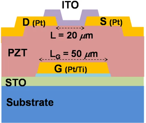
We fabricated a FGT with a bottom-gate and bottom-contact configuration, as shown in Fig. 1.
Fig. 1. Schematic drawing of the FGT with a bottom-gate and top-contact configuration.
Second, a 160-nm-thick PZT film having a composition of Pb1.2Zr0.4Ti0.6O3 was prepared by a sol-gel
method. The PZT film was consolidated at 400 oC for 15 min, and then crystallized at 500 oC for 30 min in air atmosphere to obtain a (111)-preferred orientation. Third, a 100-nm-thick Pt film was formed as the source and the drain electrodes of the FGT by sputtering. Next, a 5%wt Sn-doped ITO precursor solution (Kojundo chemical laboratory company, Japan) was spin-coated, dried at 250 oC for 5 min, and consolidated at 400 oC for 15 min to form the ITO film. Thereafter, the ITO film channel area was isolated by reactive ion etching. The channel length (L), channel width (W) and gate length (LG) of the fabricated FGT were 20, 60 and 50 µm, respectively. Finally, the ITO channel was
crystallized in air atmosphere by using rapid thermal annealing. We found that, if the annealing temperature was higher than 450 oC, the on/off current ratio decreased because of the strong diffusion at the ITO/PZT interface and of the difficulty in depletion for the FGT with a high conductive ITO channel. Also, the off current became large due to a large gate leak from the channel area. On the other hand, if the annealing temperature was a little bit lower than 450 oC, the memory window of the FGT was narrow due to the poor crystallinity of the ITO film. As a result, the best operation of the FGT corresponded to an ITO channel annealed at 450 oC for an hour, for which the carrier concentration, resistivity and thickness were 1018 cm-3, 0.3 Ωcm and 25 nm, respectively.
3. Results and discussion
Figure 2(a) shows the thermogravimetry and differential thermal analysis (TG-DTA) profile of the ITO precursor solution, measured by using TG-DTA8120 model, Rigaku, Japan. The first endothermic reactions with large weight losses were observed at 90 oC due to solvent evaporation. The exothermic peak at 408 oC without weight loss corresponds to the crystallization of the ITO. According to the TG-DTA result, the ITO crystallization temperature is rationalized to be around 450 oC from the viewpoint of a low-temperature process. Figure 2(b) shows a cross-section transmission electron microscope (TEM) image at the channel area of the FGT on the PZT/Pt/Ti/STO/SiO2/Si substrate, which was
observed by using H-7100 model, Hitachi, Japan. It is found that the sol-gel process ITO and PZT films were grown dense enough on the Pt bottom gate. The insert of Figure 2(b) shows a larger-scale image at the ITO/PZT interface. It is obvious that there is no serious reaction between the ITO and PZT films, which strongly supports the operation of the FGT. One notices on the FGT structure (see Figure 1) that, the ferroelectric-gate PZT layer is not only grown on the Pt bottom gate, but also on the STO film layer to isolate each FGT cell in the integration circuit. Thus, we fabricated FGTs on both a pc-STO/SiO2/Si substrate and a sc-STO(111) wafer as a comparison of transistor operation. In
this study, the PZT film was preferentially (111)-oriented on a Pt(111) film or on a sc-STO(111) wafer, and was randomly-oriented on a pc-STO/SiO2/Si substrate, although the XRD results were not
shown here.
Figure 3(a) and (b) shows polarization-applied voltage (P-V) hysteresis loops of the 160-nm-thick PZT film measured from FGTs on the pc-STO/SiO2/Si substrate and on the sc-STO(111) wafer,
One can observe that both P-V loops have a good squareness and symmetry. The remnant polarization (Pr) of the PZT film is 22 µC/cm
2
for the FGT on the pc-STO/SiO2/Si substrate, which is lower than
the Pr of 31 µC/cm
2
for the FGT on the sc-STO(111) wafer. This is because the crystalline quality of PZT and Pt films on the pc-STO/SiO2/Si substrate is worse than that on the sc-STO(111) wafer as
mentioned above.
Fig. 2. (a) TG-DTA profile of the ITO precursor solution and (b) cross-section TEM image at the channel area of the FGT.
Fig.3.bmp
Fig. 3. Polarization-applied voltage (P-V) hysteresis loops for the FGTs fabricated on: (a) a poly-crystalline STO/SiO2/Si substrate and (b) a single crystalline STO(111) wafer.
Figure 4(a) and (b) shows the transfer characteristics (ID-VG) of FGTs fabricated on the
7 V and returned to -7 V at a constant drain voltage VD of 1.5 V. The ID-VG curves imply a typical
n-channel transistor with a counter-clockwise hysteresis loop, indicated by arrows, which exhibits a clear memory function of FGTs originating from the nature of ferroelectric materials. Here, we can estimate the memory window to be about 2 V, which is almost equal to the twice coercive voltages (2Vc∼2 V) shown in Figure 3. This is theoretically reasonable and indicates the effectiveness of the
low-temperature process (450 oC) for the sol-gel ITO channel because the well-formed ITO/PZT interface causes a small trap density, and the pining domains might be negligible at the ITO/PZT interface. Next, we can see in Fig. 4(b) that the drain current of the FGT on the sc-STO(111) wafer is saturated easily and that the ID-VG loop is square, which are better than those of the FGT on the
pc-STO/SiO2/Si substrate shown in Fig. 4(a). This behavior is consistent with that shown in Fig. 3, where
the polarization for the FGT on the sc-STO(111) wafer is also saturated more easily, and where the P-V loop is more square. This indicates that the shape of the ID-VG loop is related to that of the P-V loop,
i.e., the crystalline and ferroelectric quality of the PZT film is important for the FGT operation. From Fig. 4, we can also see that the on/off current ratio for the FGTs is about 105 and 106 on the pc-STO/SiO2/Si substrate and the sc-STO(111) wafer, respectively. When VG < 0, the “off” current is less
than 10-10 A for the FGT on pc-STO/SiO2/Si substrate and less than 10 -8
A for the FGT on the sc-STO(111) wafer. These off currents are lower than that of the sputter-ITO channel FGT (>10-8 A), as we reported before, even though the thickness of the sol-gel ITO film (25 nm) is thicker than that of the sputter ITO film (10 nm) [5]. We are convinced that the sol-gel ITO channel can be depleted more easily due to a lower conductivity and a lower carrier concentration, compared with the sputter ITO channel.
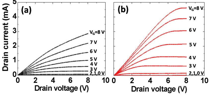
Figure 5(a) and (b) shows the output characteristics (ID-VD) of the FGTs on the pc-STO/SiO2/Si
substrate and on the sc-STO(111) wafer, respectively, which were tested by a semiconductor parametric analyzer (Agilent 4155C). The VD was swept from 0 to 8 V, while the VG was also
increased from 0 to 8 V with a step of 1 V. It is interesting to note that a typical n-channel transistor operation with a very large “on” saturated current up to 3 and 4.6 mA was obtained when VG = VD = 8
V on the pc-STO/SiO2/Si substrate and on the sc-STO(111) wafer, respectively. These values are
larger than the ID of 2.5 mA obtained from the FGT with a sputter ITO channel [5]. Also, it is much
larger than the ID of 0.8 mA at large operation voltages VG = VD = 100 V from the TFT with a sol-gel
ITO channel and SiO2 gate insulator as reported by Kim et.al [12]. Based on this work, the field-effect
mobility (µFE) of the sol-gel ITO channel FGT was estimated to be 8.0 cm2/Vs for the FGT on the
sc-STO(111) wafer. This µFE is a little smaller than that of the sputter ITO channel FGT, of which µFE is
9.1 cm2/Vs [5]. Also, it is comparable with other solution-processed channels, e.g. the ZnO-based TFT (<0.8 cm2/Vs), [7,8] the IGZO-based TFT (<7.9 cm2/Vs) [9], the IZO-based TFT (7.3-16.1 cm2/Vs) [10,11], and the ITO-based TFT (around 10 cm2/Vs) [12]. Furthermore, we estimate the saturated drain current per unit gate width is about 0.03 mA/um at operation voltages of 5 V from this work, which is comparable to that obtained from the conventional MOSFET with the same channel length. This supports that the sol-gel ITO channel FGT is very expected to the LSI downscaling because its structure is one simple transistor and the large output signal is obtained mainly due to the huge induced charge of the ferroelectric gate compensated to the small mobility of the sol-gel ITO channel. This is different from the MOSFET, of which the on current is mainly contributed from the large mobility of the Si channel.
4. Conclusion
In summary, we obtained an excellent operation for the FGTs fabricated on both a pc-STO/SiO2/Si
substrate and a sc-STO(111) wafer, in which the ITO channel was prepared by a solution-processed method and annealed only at 450 oC. In particular, we demonstrated a typical n-channel FGT with a square transfer characteristic loop, whose on/off current ratio is larger than 105, and whose memory window is 2 V. It is interesting that a large saturated “on” current as high as 4.6 mA can be achieved at operation voltages of 8 V. From the achievement, we believe that the FGT with a solution-processed ITO channel and PZT ferroelectric-gate insulator proposes a new challenge for the future of nonvolatile ferroelectric memory devices, which directly support to data decoding, without any amplifier.
Acknowlegment
This research is funded by Vietnam National Foundation for Science and Technology Development (NAFOSTED) under grant number 103.02-2012.81. We are thankful to the measurements assistance from Japan Science and Technology Agency, ERATO, Shimoda Nano-Liquid Process Project.
References
[1] Y. Kato, Y. Kaneko, H. Tanaka, and Y. Shimada, Nonvolatile Memory Using Epitaxially Grown Composite-Oxide-Film Technology, Jpn. J. Appl. Phys., 47 (2008) 2719.
[2] Y. Kaneko, H. Tanaka, M. Ueda, Y. Kato, and E. Fujii, A dual-channel ferroelectric-gate field-effect transistor enabling NAND-type memory characteristics, IEEE Trans. Electron Devices, 58 (2011) 1311.
[3] Y. Kaneko, Y. Nishitani, M. Ueda, E. Tokumitsu, and Eiji Fujii, A 60 nm channel length ferroelectric-gate field-effect transistor capable of fast switching and multilevel programming, Appl. Phys. Lett., 99 (2011) 182902. [4] M.W. Prins, S.E. Zinnemers, J.F.M. Cillessen, and J.B. Giesbers, Depletion-type thin-film transistors with a
ferroelectric insulator, Appl. Phys. Lett., 70 (1997) 458.
[5] T. Miyasako, M. Senoo, and E. Tokumitsu, Appl. Phys. Lett., Ferroelectric-gate thin-film transistors using indium-tin-oxide channel with large charge controllability, 86 (2005) 162902.
[6] T. Shimoda, Y. Matsuki, M. Furusawa, T. Aoki, I. Yudasaka, H. Tanaka, D. Wang, M. Miyasaka, and Y. Takeuchi, Solution-processed silicon films and transistors, Nature, 440 (2006) 783.
[7] D. Gupta, M. Anand, S.W. Ryu, Y.K. Choi, and S.H. Yoo, Nonvolatile memory based on sol-gel ZnO thin-film transistors with Ag nanoparticles embedded in the ZnO/gate insulator interface, Appl. Phys. Lett., 93 (2008) 224106.
[8] H.C. Cheng, C.F. Chen, and C.Y. Tsay, Transparent ZnO thin film transistor fabricated by sol-gel and chemical bath deposition combination method, Appl. Phys. Lett., 90 (2007) 012113.
[9] G.H. Kim, B.D. Ahn, H.S. Shin, W.H. Jeong, H.J. Kim, and H.J. Kim, Effect of indium composition ratio on solution-processed nanocrystalline InGaZnO thin film transistors, Appl. Phys. Lett., 94 (2009) 233501.
[10] C.G. Choi, S.J. Seo, and B.S. Bae, Solution-processed indium-zinc oxide transparent thin-film transistor, Electrochem. Solid-State. Lett., 11 (2008) H7.
[12] H.S. Kim, M.G. Kim, Y.G. Ha, M.G. Kanatzidis, T.J. Marks, and A. Facchetti, Low-Temperature Solution-Processed Amorphous Indium Tin Oxide Field-Effect Transistors, J. Am. Chem. Soc., 131 (2009) 10826. [13] T. Miyasako, B.N.Q. Trinh, M. Onoue, T. Kaneda, P.T.Tue, E. Tokumitsu, and T. Shimoda, Totally
solution-processed ferroelectric-gate thin-film transistor, Appl. Phys. Lett., 97 (2010) 173509.
[14] P.V. Thanh, B.N.Q. Trinh, T. Miyasako, P.T.Tue, E. Tokumitsu, and T. Shimoda, Electric Properties and Interface Charge Trap Density of Ferroelectric Gate Thin Film Transistor Using (Bi,La)4Ti3O12/Pb(Zr,Ti)O3 Stacked Gate Insulator, Jpn. J. Appl. Phys., 51 (2012) 09LA09.