Effect of Thickness on Catalytic Performance of Cu Doped TiO
2Thin
Films
Vidhya.R1, Gandhimathi.R2, Sankareswari.M1, Neyvasagam.K3*
1Department of Physics, V.V. Vanniaperumal College for Women, Virudhunagar, India.
2Department of Physics, AMET University, Kanathur, Chennai, India.
*3PG and Research Department of Physics, The Madura College, Madurai, India.
Email id: srineyvas@yahoo.co.in
Abstract
Thickness plays a vital role in determining properties of thin films and its variation influences performance of the thin films remarkably. In this work, the impact of thickness on the structural, morphological and optical properties of Cu-TiO2 thin
films have been investigated in detail. Copper doped Titanium dioxide thin films with different thickness (~1.89 to 2.44µm) were deposited on glass substrates by sol gel dip coating technique and were annealed at 500°C for 3 h. The annealed films were subjected to different characterization studies. The surface morphology and stoichiometry of the prepared films were characterized by Scanning Electron Microscopy (SEM) and Energy Dispersive X-ray spectroscopy (EDX) respectively. The microstructural parameters such as crystallite size, dislocation density and micro strain of deposited films demonstrate notable variations with increased film thickness. The optical absorption of Cu-TiO2
thin films show shift towards long wavelength region depending upon thickness. The photocatalytic activity of the different layered thin films was also tested via the degradation of Methylene Blue (MB) and Methylene Orange (MO) dye solutions under visible irradiation. The threshold thickness for best catalytic efficiency was acquainted and reported.
Keywords: Cu-TiO2 thin films, XRD, SEM,
UV-Visible, Photocatalytic activity
1. Introduction
Due to the increase in the demand of thin films in diverse fields such as semiconductor device fabrication, optical coating, magnetic recording, photovoltaics and photocatalytic turn out thin film
techniques as one of primary materials processing methods. The fundamental properties of thin films rely on deposition parameters such as film thickness, grain size and substrate quality. The transition metal oxide TiO2 semiconductor possesses a range of
applications in various fields due to its exceptional properties such as nontoxicity, high catalytic activity, low cost, and long-term stability [1, 2]. TiO2 has
been synthesized using numerous methods such as chemical vapor deposition (CVD), plasma, hydrothermal and sol-gel [3]. Among these methods, sol-gel is the simplest technique in which the different material parameters such as morphology, surface area, average crystallite size and phase structure can be controlled and extended in determining photocatalytic activity of TiO2 compound [4].
Pristine TiO2 has band gap energy of about 3.2eV.
TiO2 photocatalyst stimulates production of highly
oxidative hydroxyl radicals (OH) and Super-oxide radicals (O2-), resulting in the decomposition of any
organic pollutants present in the environment through a natural occurring oxidation process. Thus, TiO2 have gained considerable attention as a
self-cleaning material for environmental purification and clean energy. The key factors governing the photocatalytic activity of TiO2 are lowering of band
gap energy in visible region and prevention of electron hole recombination rate. One of the methods to improve photocatalytic activity of TiO2
in the long wave length region is doping metal impurities in the TiO2 matrix or coupling low band
gap semiconductor with TiO2 [5-7]. The integration
of metal ions in TiO2 lattice bids a way to trap the
charge carrier thus improving the efficiency of TiO2
In this work, efforts have been taken to prepare Cu doped TiO2 thin films of different thickness by
sol-gel dip coating method and the influence of thickness on optical and catalytic properties of Cu-TiO2 thin films was investigated effectively.
Materials and methods 2.1. Raw materials
Titanium (IV) isoproxide (TTIP, 99.95 %, Fluka Sigma-Aldrich), and copper (II) nitrate trihydrate (Cu(NO3)2.3H2O) were used as raw materials to
prepare Cu-TiO2 thin films. Ethanol (C2H5OH,
99.9%, Merck Germany) was used as solvent in the preparation of samples.
2.2. Thin films preparation
Cu doped TiO2 thin films of various thicknesses
(5, 7 & 9 dipping cycles) were prepared via sol-gel dip coating method. In the beginning 2.8 ml of Titanium (IV) isoproxide (TTIP) was mixed with 20 ml of ethanol and the mixture was vigorously stirred at room temperature for 10 min. And then 0.6 ml of acetic acid was added drop by drop to this solution and the blend was stirred for another 10 min. A suitable amount of copper (II) nitrate trihydrate was added into this solution slowly. Eventually, it was stirred at room temperature for 90 min., until clear sol was formed. To fabricate 5 dip Cu-TiO2 thin films, the sol was deposited on glass
substrates by five dipping with the drawing speed of about 1.5 mm/s at room temperature and the process was repeated to obtain 7 & 9 dip thin film samples of different thickness. The coated specimens were calcined at the temperatures of 500°C for 3 h with a heating rate of 10°C/min. The thickness was measured by surface profile meter. The thickness of films of 5, 7 & 9 dip is about 1.89, 2.17 & 2.44 µm respectively.
2.3. Characterization
The crystallite size of the Cu-TiO2 thin films
prepared with different Cu concentrations were estimated by X–Ray Diffraction method (XRD) using X’PERT PRO X–ray diffractometer which was
operated at 40 KV and 30 mA with CuKα1 radiation of wavelength 1.5407Å. UV–visible spectra were recorded in the range of 300 – 800 nm using the Schimadzu 1800 UV–VIS–NIR spectrophotometer. The surface morphology observation and elemental were done by Carl Zeiss and Supra 55 respectively.
The surface topology was studied using Atomic Force microscope (AFM) Nano surf Easy scan 2. The thickness of the film was measured using Mitutoyo Surfest SJ-301stylus profilometer. Photocatalytic activity of the prepared Cu-TiO2 thin films was studied by
examining the degradation of aqueous solution of methylene blue (MB) under visible light irradiation using 500-W halogen lamp.
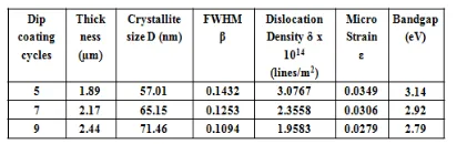
3. Results and Discussion 3.1. XRD Analysis
The XRD patterns of Cu doped TiO2 thin films are
shown in Figure1. It confirmed the presence of anatase phase of tetragonal structure with high intensity peak in (101) orientation. The other orientations observed at (210), (200) and (105) for all samples with low intensities, agree with JCPDS file no. 89-4203. Cu compound phase cannot be found in the XRD peaks due to small amount of Cu doping. The calculated micro structural parameters such as crystallite size, micro strain and dislocation density are tabulated in Table 1. The variation in dislocation density and micro strain with the thickness of films is shown in Figure 2. The reduction in FWHM reveals that the crystallization becomes more perfect when the thickness of film was increased by depositing more layers of Cu-TiO2 on the
Figure 1. XRD patterns of Cu-TiO2 thin films for
different number of coatings
Figure 2. Variation of Dislocation density and Microstrain with different dipping cycles
Table 1. Micro structural parameters of Cu-TiO2
films deposited at different dipping cycles
3.2. Surface morphology and Quantitative Analysis The surface morphology of deposited films was investigated by scanning electron microscope. Figure 3a & 3b show the SEM images of Cu doped TiO2 thin
films coated with 5 & 7 dip cycles. The images illustrate irregular flake like cracked morphology. During deposition, films undergo significant tensile stress which is relieved as cracks by annealing [11].
The surface cracks gradually rise with the increase in coating cycles. The EDAX picture shown in Figure 3c depicts only characteristic peaks of Ti, O and Cu elements.
Figure 3. SEM images of the film deposited for 5 coatings (a) and 7 coatings (b) of Cu-TiO2 thin films
with EDAX spectrum (c)
3.3. Surface topography
Atomic force microscope was used to characterize the surface morphology and roughness of the deposited samples. The AFM image of Cu doped TiO2 (9 dip) is shown in Figure 4. We can see
dispersal of aggregated spherical grains of different sizes on the surface. The surface roughness parameters values such as the root mean square roughness (Rq) and average roughness (Rave) are
calculated as 11.26 nm and 8.567nm respectively.
Figure 4. AFM (a) 2D and 5 (b) 3D image of Cu-TiO2
3.4. Optical analysis
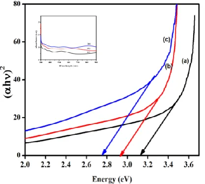
The UV-Visible optical absorption spectra of the copper doped TiO2 thin films are shown in Figure 5.
Depositing more layers of Cu-TiO2 films (5 to 9
dipping) resulted in shifting the absorption edge towards the visible region up to 440nm. The shift in the absorption edge is attributed to change in the crystallite size and thin film density with various thickness [12]. Also, the absorption edge movement towards longer wavelengths represents a decrease in the bandgap of about ~0.35eV [13]. Thus, the addition of Cu-TiO2 layers on the substrate alter the
optical responses of samples, causing a decrease in the bandgap energy and resulting in wide range absorbance of visible light, which can be used in photocatalytic application.
Figure 5. Direct bandgap of Cu-TiO2 thin films (a)
5dip (b) 7dip & (c) 9dip
3.5. Photocatalytic activity
3.5.1. Thickness effect on photocatalysis
Photocatalytic activity of Cu doped TiO2 thin
films was analysed by examining the degradation of methylene blue (MB) and methylene orange (MO)
dye solutions. The thin films were soaked into dye solutions and kept under visible light for irradiation. After that the 5ml of the degradation solution was taken and subjected to Schimadzu-1800 UV-Vis spectrometer to measure the absorbance.
To analyze the effect of thickness on catalytic performance, the thin films with different thicknesses were dipped into MB solution and kept under irradiation for 3hour.The absorbance spectra of degraded MB with Cu-TiO2 thin films of different
thickness are shown in Figure 6a. The reduced band gap energy and increased surface roughness (act as reaction sites) play important role in determining catalytic efficiency [14, 15]. It was observed that the photocatalytic activity of Cu-TiO2 film was
depending on the thickness. All the three films show degradation effect but the film with 5 coatings depicts the more enhanced catalytic activity than other films. The amount of photo generated electron hole pairs reaching the surface is abridged when thickness of the film increases above 1.89 µm. It was found that the thickness of Cu-TiO2 (5-dip) film is
Figure 6 (a). Optical absorption spectra of degradation of MB dye thin films (b) Percentage of
degradation of MB for different thickness of the films
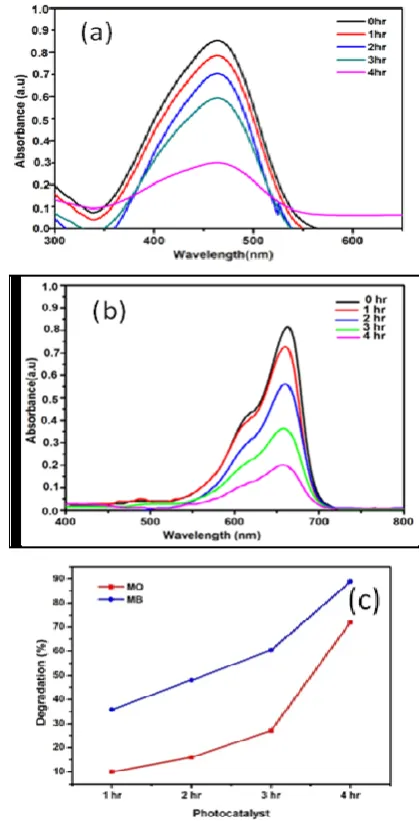
3.5.2. Time Effect on photocatalysis
The degradation time effect on MB and MO dyes was examined by soaking Cu-TiO2 thin films in MB
and MO solutions respectively for 1, 2,3 and 4hour under visible light. The changes in the concentration of dye solutions MB and MO as a function of time with Cu-TiO2 catalyst are shown in Figure 7(a & b).
In photocatalytic activity, the degradation efficiency is more reliant on the illumination time. If the illumination time is longer, the degradation will be higher. The degradation efficiency increases with increase time with Cu-TiO2 thin films. Figure 7c
shows degradation percentage of MB & MO dye with the catalyst Cu-TiO2 (5dip). It was seen that
complete decomposition took place in MB solution after 240 minutes. Hence, the optimum illumination time for degradation of MB is 240 minutes. However, in MO solution, we could see still the presence of little dye after 240 minutes degradation. Thus, it is resolved is that Cu-TiO2 catalyst was more
efficient for the degradation of MB.
Figure 7 (a & b) . Optical absorption spectra of degradation of MO & MB dye thin films (b) Percentage of degradation of MO & MB for
Cu-TiO2 films
This work reveals dependences of structural, optical and degradation properties on the thickness of Cu-TiO2 films deposited onto glass substrates by
dip coating technique. The thin films exhibited homogeneous surface grain aggregation, improvement in the optical activity and reduced bandgap energy. Degradation of MB dye solution under visible light rationalizes the dependence of thickness of Cu-TiO2
thin films on the photocatalytic activity property. The film with ~1.8µm thickness (5-dip) show better degradation efficiency since only the excitons present in the surface region of few nm involves vigorously in photo catalytic reactions. Degradation time effect analysis shows that the film removes more MB molecules in short time. Hence it is proposed that Cu-TiO2 thin film (~1.89µm) can act as an excellent
photocatalyst under visible-light excitations.
References
[1] M.E.Yang Juan, Sen and J.M.F. Ferreira Hydrothd, Synthesis of nano sized Titania powders: Influence of tetra alkyl ammonium hydroxides on particle characteristics, J. Am. Ceram. Soc. 84(8), 2001, pp.1696-1706.
[2] Hang Ru-bin and Gao Lian, Effect of peptization on phase transformation of TiO2 nanoparticles, J.
Mater Res Bull., 36, 2001, pp.1957- 1965.
[3] M.R. Hoffman, S.T. Martin, W. Choi, D.W. Bahnemann, Environmental applications of semiconductor photocatalysis, Chemical Reviews, 95, 1995, pp69.
[4] D. Byun, Y. Jin, J. Kim, K. Lee, P. Hofmann, Photocatalytic TiO2 deposition by chemical
vapour deposition, J. Haz. Mater., 73, 2006, pp.199.
[5] X. Chen. S.S. Mao, Titanium dioxide nanomaterials synthesis, properties, modifications
and applications, Chemical Reviews, 107, 2007, pp.2891.
[6] T.C. Dang, D.L. Pham, H.C. Le, V.H. Pham, TiO2/CdS nanocomposite film: Fabrication,
characterization, electronic and optical properties, Advances in Natural Sciences: Nanoscience and Nanotechnology 01, 2010, pp.5002.
[7] B. Tryba, M Piszcz, A.W. Morawski, Photocatalytic activity of TiO2-WO3 composites,
Hindawi Publishing Corporation, International Journal of Photoenergy Volume 2009, Article ID 297319, pp.7.
[8] P. Dharmarajan, A. Sabastiyan, M. Yosuvasuvaikin, S. Titus and C. Muthukumar, Photocatalytic Degradation of Reactive Dyes in Effluents Employing Copper Doped Titanium Dioxide Nanocrystals and Direct Sunlight, Chem Sci. Trans, 2(4), 2013, pp.1450-1458.
[9] P. Malliga, J. Pandiarajan, N. Prithivikumaran, K. Neyvasagam, Influence of Film Thickness on Structural and Optical Properties of Sol – Gel Spin Coated TiO2 Thin Film, IOSR Journal of
Applied physics, 6, 2014, 22-28.
[10]Effect of Film Thickness on Structural and Electrical Properties of Sputter-Deposited Nickel Oxide Films Hao-Long Chen, Yang-Ming Lu and Weng-Sing Hwang, Materials Transactions, Vol. 46, No. 4, 2005, pp. 872 - 879.
[11]Senjiang Yu, Xiaofei Zhang, Xiaofei Xiao, Hong Zhou and Miaogen Chen, Wrinkled stripes localized by cracks in metal films deposited on soft substrates, Soft Matter, 11, 2015, pp.2203-2212
Properties Dependence on Thickness of Screen-Printed TiO2 Thin Films, Journal of Materials
Physics and Chemistry, 4, 2016, pp.1-3.
[13]Gurpreet Kaur, AnirbanMitra, K.L.Yadav, Pulsed laser deposited Al-doped ZnO thin films for optical applications, Progress in Natural Science: Materials International, 25, 2015, pp.12-21.
[14]Yen-Hua Chen and Kuo-Jui Tu, Thickness Dependent on Photocatalytic Activity of Hematite Thin Films, International Journal of Photoenergy, 2012, Article ID 980595, pp.6.
[15]Masoud Rismanchian, Farideh Golbabaei, Yadollah Mortazavi, Gholamhossein Pourtaghi, Abbas Rahimi Foroushani, and Parvin Nassiri, A Comparative Evaluation of TiO2 Suspension