http://www.sciencepublishinggroup.com/j/nano doi: 10.11648/j.nano.20180601.12
ISSN: 2575-3754 (Print); ISSN: 2575-3738 (Online)
Selective Pattern Transfer of Nano-Scale Features
Generated by FE-SPL in 10 nm Thick Resist Layers
Martin Hofmann
1, *, Cemal Aydogan
1, 2, Claudia Lenk
1, Yana Krivoshapkina
1, Steve Lenk
1,
Burkhard Volland
1, Marcus Kaestner
1, Burhanettin Erdem Alaca
3, Eberhard Manske
4,
Ivo Rangelow
11
Department of Micro- and Nanoelectronic Systems, Ilmenau University of Technology, Ilmenau, Germany
2
Department of Electronics and Cryptology, TUBITAK - YITAL, Kocaeli, Turkey
3Department of Mechanical Engineering, Koc University, Istanbul, Turkey 4
Department of Process Measurement and Sensor Technology, Ilmenau University of Technology, Ilmenau, Germany
Email address:
*Corresponding author
To cite this article:
Martin Hofmann, Cemal Aydogan, Claudia Lenk, Yana Krivoshapkina, Steve Lenk, Burkhard Volland, Marcus Kaestner, Burhanettin Erdem Alaca, Eberhard Manske, Ivo Rangelow. Selective Pattern Transfer of Nano-Scale Features Generated by FE-SPL in 10 nm Thick Resist Layers. American Journal of Nano Research and Applications. Vol. 6, No. 1, 2018, pp. 11-20. doi: 10.11648/j.nano.20180601.12
Received: January 8, 2018; Accepted: January 20, 2018; Published: March 7, 2018
Abstract:
High performance single nanometer lithography is an enabling technology for beyond CMOS devices. In this terms a novel mask- and development-less patterning scheme by using electric field, current controlled Scanning Probe Lithography (FE-SPL) in order to pattern structures on different samples was developed. This work aims to manufacture nanostructures into different resist by using FE-SPL, whereas plasma etching at cryogenic temperatures is applied for an efficient pattern transfer into the bottom Si substrate. The challenge for future quantum devices, generated by SPL and cryogenic etching, is finding a resist that is at most 10 nm in thickness and has a plasma durability high enough for pattern transfer into silicon. As a first step towards future quantum devices the silicon-to-resist selectivity of calixarene, AZ Barli, poly (3-hexylthiophen-2, 5-diyl) and polymethylmethacrylat for the anisotropic cryogenic dry etching process was estimated. A silicon-to-resist selectivity of about 4:1 for each of these resists was found. With these results, nano-scale, highly parallel double line features in silicon for future double patterning were generated.Keywords:
Field Emission Scanning Probe Lithography, Cryogenic Plasma Etching, Single-Electron Devices1. Introduction
Scaling down of device sizes has been the fundamental strategy for improving the performance and efficiency of nanoelectromechanical devices and systems (NEMS). Field-Emission Scanning Probe Lithography (FE-SPL) permits a precise and cost effective fabrication route towards the enabling of new devices as, e.g., single electron transistors [1]. Thereby, a Fowler-Nordheim-type electron emission of low energy electrons from a sharp scanning tip is caused by an intense electric field [2]. In contrast to EBL, in which high energy electrons are generating secondary electrons which induce the lithographic reaction, in FE-SPL electrons in an energy range (typically < 50eV) just needed for chemical
patterning, and tone switching without post processing [3, 4]. Moreover, a reliable dry etching recipe operating at cryogenic temperatures for pattern transfer into silicon using a relatively thin resist layer of calixarene, (usually with thicknesses of 10 to 50 nm) and preserving the lithographic resolution was developed. Thereby, the combination of cryogenic temperatures with the reactive ion etching using SF6 with a certain amount of oxygen enables a highly
anisotropic and pattern preserving etching. The process is established for aspect ratios and linewidths below 10 nm and for high aspect ratio (HAR) in the 50-100 nm regime respectively.
In this work results from the optimized lithography and etching protocols as well as tests of the plasma durability and etching stability of different resists typically used for lithography purposes will be presented.
2. Field-Emission Scanning Probe
Lithograhpy
For pattern generation of nano-scale features into ultrathin resists, field-emission scanning probe lithography (FE-SPL) is used. An applied bias voltage between tip and sample generates an electric field. Due to the enhancement of the field caused by the ultrasharp tip [2], a constant Fowler-Nordheim electron emission can occur. These electrons are used to generate features in the resist.
(a)
(b)
Figure 1. (a) SEM image of the thermomechanically actuated piezoresistive cantilever. (b) A sub-10nm write and imaging resolution by SPL/AFM require cantilever tips with radius of curvature of < 15 nm [5].
The utilization of self-actuated, self-sensing active cantilevers with a resonance frequency of about 100 kHz, enables not only to structure the resist with FE-SPL but also to inspect the written features by AFM. The oscillation of these cantilevers is induced thermomechanically, whereas the deflection is measured by piezoresistors. The thermomechanical actuator, as indicated in Figure 1 (a) by yellow color, actuates the cantilever on the basis of the bimorph effect. It consists of a metallic micro heater, which excites the cantilever at its resonance, and simultaneously deflects the cantilever at lower frequencies off-resonance (1 Hz to 20 kHz). In this respect, the cantilever bends proportionally to the square of the input DC-current to the micro-heater. The deflection read-out of the cantilever is realized by piezoresistive sensors integrated on the base of cantilever beam (colored green in Figure 1 (a)) [5- 9]. Four piezoresistors are arranged in an integrated Wheatstone bridge configuration to reduce the influence of temperature variations and noise. At the end of the cantilever beam a sharp conductive tip with typically < 15 nm tip radius of curvature is integrated (Figure 1 (b)). The shape of the tip has considerable influence on the electric field and the trajectories of the electrons [10], as well as on the emission probability [2]. A more detailed information about the active cantilever, their fabrication process as well as their performance is provided in [9].
The use of self-sensing and self-actuated scanning probes enables the implementation of two independent feedback loops in the setup: The first is the feedback loop for the AFM, to image patterns in high resolution and perform surface inspection. Here the height of the scanning probe is regulated in dependence of the amplitude of oscillation. The second is a current feedback for FE-SPL, where the height of the scanning probe is changed to keep the current setpoint. With the combination of these 2 loops, the surface can be inspected and structured with the same scanning probe.
The SPL tool operates in constant-current Fowler-Nordheim regime, thus pattern generation into the resist is done by a fine beam of low energy electrons (a few eV<E<50 eV) and results in either development-less positive tone or negative tone behavior, dependent on the type of resist and the electron dose. The principle can be seen in Figure 2. The linewidth of the generated patterns can be regulated by the electron dose. To adjust the favored electron dose, the FE-SPL tool is capable of setting both, current and writing speed. The resulting line dose can be calculated as
,
Figure 2. Concept of closed-loop for imaging and patterning. Figure according to [4].
Beside the electron dose, the distance between tip and sample is important for a stable lithographic process. The tip-to-sample distance can be regulated by the applied voltage (at a constant current setpoint), whereby a higher voltage causes a higher distance and vice versa. The bias voltage can be regulated in the range of 5 V to 100 V. The optimal bias voltage value thereby depends on the resist, resist thickness, substrate and tip.
It should be mentioned that the environmental conditions should be stable during the lithography process. The optimal temperature and humidity is in the range of 22°C ± 2°C, 35 % ± 10 %, respectively. Large fluctuation of the environmental conditions can cause a change of tone or even a tip crash. The general setup of the FE-SPL tool is shown in Figure 3. The system is based on a granite block and a damping system to minimize thermal and mechanical drift. The top scanner for the regulation of the scanning probe height is mounted on a cross-beam suspension for higher mechanical stability. Two different scanners can be applied; one providing a 10 × 10 µm2 scan area and another with 200 × 200 µm2 scan area. The sample is located on a coarse positioning bottom stage to enable an increased patterning area of up to 100 × 100 mm2 size. A step-and-repeat function enables an active pattern area up to 4 inch wafers [1]. The step-and-repeat function is mostly used to generate same
structures repeatedly on the sample. By optical navigation through a camera mounted on the top of the system, structures can be found easily.
The aim of the FE-SPL is
(a) scaling down the nanomanufacturing to the single nanometer,
(b) development of nano-lithographic methods with respect to cost efficiency and reliability,
(c) to realize ultra-low power electronics, single electron transistors, quantum devices and individual atom manipulation and
(d) to create new technology for beyond CMOS devices with help of cost-efficiencies, to implement mix-and-match technique.
Figure 3. Cross-beam setup combining top scanner and bottom coarse positioning stages enabling a step-and- repeat-based SPL scheme.
3. Cryogenic Etching
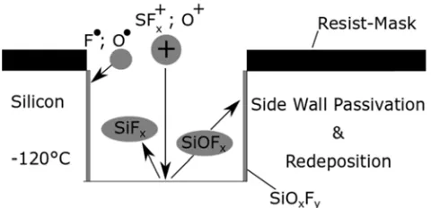
For a pattern transfer in the nanoscale range, a cryogenic anisotropic etching procedure is used. This process has been first introduced by Tachi et al. [13] and many studies [14-16] revealed enhancements of the cryogenic etching process compared to standard reactive ion etching (RIE). Basically, the idea of cryogenic etching is to combine the effect of ionized feed gases with low substrate temperatures [17]. The low temperature increases the sticking probabilities of the reactants and enables the formation of a polymeric layer on the silicon surface [18]. In this work, SF6/O2 gases at
cryogenic temperatures are used. These feed gases are commonly used for deep anisotropic etching of silicon. In this particular process, both oxygen and the low temperature are necessary to produce the passivation layer at the feature sidewalls. By lowering the temperature below - 100°C, recombination of Si, O, and F becomes energetically favorable and SiOxFy molecules are created. Furthermore, the
attack of sidewalls by radicals and the evaporation rate of halogen compounds such as SiOxFy products are thermally
activated by an Arrhenius law for activation energy, hence these rates are reduced when the substrate temperature is lowered [18]. This results in a polymeric SiOxFy passivation
layer on the silicon surface at cryogenic temperatures. This layer protects the silicon from the spontaneous etching by the fluorine. Due to the condensation of Si2F6 products on the
silicon surface, the spontaneous etching of Si by fluorine is blocked at temperatures lower than -196°C [19]. Thus the practically usable temperature is limited. For the cryogenic etching process, the typical temperature range is between - 100°C to -140°C [17].
To this point, the passivation layer acts as an etch stop, because the layer hinders further etching in both vertical and horizontal direction. Thus, additionally to the chemical etching, a sputtering effect is applied by a potential difference between plasma bulk and sample surface. This triggers an acceleration of ions straight towards the sample [20]. These accelerated ions will have energies of a few tens
of electron-volt, depending on the actual process conditions. The vertically accelerated ions have a glancing angle of incidence to the feature sidewalls, resulting in low or no sputtering of the SiOxFy layer. On the contrary, at the bottom
of the etched feature the sputtering yield is high enough to effectively remove any polymer already deposited. Additionally, the physical sputtering due to the ion bombardment also prevents the growth of an inhibitor film. Thus the fluorine can react spontaneously on the bottom of the feature, forming volatile SiF4 molecules. This attack of
silicon by fluorine is an exothermal chemical reaction. Finally, the etching product then desorbs from the surface. As a result of the above described processes, the etching proceeds only in vertical direction (ion bombardment direction) and an anisotropic profile can be achieved. [13, 18, 20-23]. Figure 4 depicts the principle of cryogenic etching.
Figure 4. Demonstration of basic principle of ions and radicals involved in cryoetching. Figure according to [22].
In 2005 Mellhaoui et al. published a cryogenic etching test for different substrate temperatures, with or without oxygen and ion bombardment [24]. They concluded that the injection of O2 to the SF6 gas results in the formation of perfect
passivation layers on the feature sidewalls, whilst prevailing cryogenic temperature. When the temperature is increased to room temperature after etching, the SiOxFy passivation layer
becomes volatile and leads to smooth silicon sidewalls. Thus, cryogenic etching allows precise pattern transfer for sub 20 nm features with high aspect ratio. It should be noted, that it has been demonstrated, that the passivation can also be created by the injection of SiF4 and O2 [25]. Chopping-mode
etches for high aspect ratios using SF6 and O2 have also been
demonstrated [26]. Since cryogenic etching is basically a reactive ion etching (RIE) process, it suffers from the same high aspect ratio effects. This effects can only be observed for features with aspect ratios >3:1. The most significant of these aspect ratio dependent effects (ARDE) are RIE-lag, bowing (barrelling), facetting and microtrenching (see Figure 5). These effects are caused by serveral mechanisms:
- Ion and kinetic neutral flux - Electron shading effect
- Transport and Depletion of chemical etch and inhibit reactants
Figure 5. The most significant aspect ratio dependent effects. Figure according to [18].
4. FE-SPL Resists
Both, lithography and the subsequent etching are affected by the resist. In this work, the influence of the pattern transfer by cryogenic etching on the FE-SPL defined pattern, more specific, the selectivity, was in the spotlight. Thus the selectivity and plasma durability of different standard FE-SPL resist will be compared.
For the creation of nanoscale features, a molecular resist is favored compared to conventional resists. Typically, calixarene resist is used for FE-SPL. Calixarenes belong to the group of metacyclophanes, are cup-shaped and the molecule size is about 1 nm. Due to its small particle size, low molecular weight, precise defined spatial extent, mono-disperse nature and high uniformity, these resists are capable of a higher resolution and lower line edge roughness for the SPL process. Furthermore, calixarene resists offer the possibility for tone switching by electron dosechanges. Due to its thermal and chemical stability [28], calixarene can be coated on rough and non-flat surfaces. It also provides high plasma etch durability, which is an important factor for the production of nanodevices [29].
Table 1. Mixing ratio and solvent for each resist taken in this work. It should be noted, that AZ Barli is weighed in ml (1 ml AZ Barli in 13 ml ELL). 1
Resist type
Amount of
resist [mg] Solvent
Amount of solvent [ml]
Layer thickness [nm]
Calixarene 70 MCB 10 20
Calixarene 35.49 MCB 10 10
AZ Barli 1 ELL 0 200
AZ Barli 1 ELL 13 10
P3HT 4 Toluol 2 10
PMMA 36.91 MIBK 10 10
Ohnishi et al. handles calixarene resists as “prospective material for nanofabrication” [30]. The following resists were compared: AZ® Barli®, Poly (3-hexylthiophen-2, 5-diyl) (short: P3HT) and Polymethylmethacrylat (short: PMMA).
PMMA is a standard resist for EBL. Details about the lithographic resolution for polymeric resists, in particular PMMA, can be found in [31]. AZ Barli is an antireflective coating for photolithography but is used as resist for FE-SPL
1 MCB: Mono Chloro Benzene; ELL: Ethyl-L-Lactate; MIBK: Methyl isobutyl ketone
as well, since it offers a small surface roughness. Due to the lithography mechanism it is necessary that either the sample or the resist is conductive. Unfortunately, all of the resist types introduced to this point are insulating. A promising loophole for future FE-SPL with non-conductive chips could be P3HT, which is a p-type semiconductor and is mainly used as part of the photoactive layer in organic solar cells or as semiconducting layer in organic field-effect transistors [32].
5. Methodology
To optimize the etching protocol and determine the etching durability of different resists, different steps were conducted. Each resist is diluted in a solvent. The corresponding solvent and mixing ratio for each resist can be obtained from Table 1.
First, a resist layer was spin-coated onto n-doped silicon chips. The parameters for spin-coating and annealing can be found in Table 2. As second step, the resist layer was structured either by FE-SPL or scratching. Next, the patterned samples are cryogenically etched. Finally, the residual resist is removed by O2-plasma.
In this work, cryogenic etching was carried out with a PlasmaPro 100 Cobra ICP cryoetching tool from Oxford Instruments. In order to obtain a passivation layer, an oxygen gas flow of 2 sccm was used. Process pressure was 5 mTorr. A DC bias voltage of 70 V and RF at 11 Watt were kept constant. The wafer is fixed to the temperature-adjusted lower electrode. The substrate temperature was -120°C.
To estimate the selectivity of different resists calixarene, AZ® Barli®, P3HT and PMMA were spun on silicon chips and annealed them (see Table 2). In result, the samples had different resists, but same thicknesses of about 10 nm upon the respective silicon samples. Lines were scratched into the resist by a scalpel and measured by AFM to obtain the resist thickness. Afterwards, each sample was etched with our cryogenic etching process for 1 minute. Then, the residual resist was removed and the final structures were analyzed by AFM and the silicon-to-resist selectivities were estimated.
To determine if there are differences in the pattern transfer process for structures obtained by scratching or FE-SPL, an additional calixarene samples with a resist layer thickness of 21 nm was prepared. These samples were patterned by FE-SPL and then imaged by AFM. For FE-FE-SPL an additional etching step was added to remove SiO2, which can be formed
on the top layer of the Si during FE-SPL due to humidity. Next, the samples were cryogenically etched for 40 s, followed by resist removal and AFM measurements to obtain the final structure depth.
principle can be seen in Figure 6. Resist areas exposed with an exposure dose larger than the ablation threshold (middle of the electron beam) are directly ablated (positive tone). Resist areas exposed with an exposure dose between the ablation and the cross-linking threshold become cross-linked (negative tone). If
the resist is wet developed, only the cross-linked regions remain on the substrate, yielding thus self-aligned features. Their distance is thereby controlled by the ablation threshold in relation to the current density of the electron beam.
Table 2. Values for spin-coating and pre-bake of different resists.
Resist type
Spin-coating Annealing
1st step 2nd step
Rotation speed duration Rotation speed duration Annealing temperature duration
rpm s rpm s °C min
Calixarene 1200 3 2000 30 130 5
PMMA 1200 3 2000 30 130 5
AZ Barli 3000 30 200 1
P3HT 3200 45 125 5
Figure 6. Generation of double line features. Due to the gaussian distribution of the electrons, resist in the center of the electron beam is exposed with a higher exposure dose than the outer beam areas, resulting in direct ablation for an exposure dose higher than the “ablation threshold” (represented by the resist colored in white) and cross-linking between “ablation threshold” and “cross-linking threshold” (indicated by resist colored in red). For exposure doses below the “cross-linking threshold” the resist remains unaffected. After wet development only the red part of the resist remains on top of the substrate.
To demonstrate the process of preparing self-aligned double-line features, lines in a meander pattern shape were written into 9 nm calixarene resist with an SPL exposure dose of 200 nC/cm. Next, the resist was wet developed, followed by the cryogenic etching process (etching time was 25 s), as mentioned in the previous section, where the remaining resist was used as etching mask, and, afterwards, residual resist was removed by an oxygen plasma. Final structures were analyzed by AFM and SEM.
6. Results
(a)
(b)
(c)
(d)
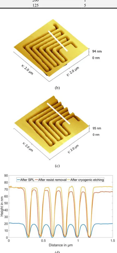
To obtain high-resolution FE-SPL patterns and fabricate future sub-10 nm structures a resist thickness of at most 10 nm will be required. Therefore, the plasma durability (silicon-to-resist selectivity) of different types of resists (calixarene, AZ Barli, P3HT and PMMA) is compared. The selectivities of the four resists were extracted from the AFM images taken after patterning, after etching and after resist removal. Examples of these AFM images in the different process steps [after FE-SPL (a), after cryogenic etching (b) and after resist removal (c)] are shown in Figure 7 for 21 nm thick calixarene resist patterned with FE-SPL.
Figure 7 d) shows the AFM profile along the contour line in Figure 7 a)-c). The initial thickness of theesist is about 21 nm (obtainable from the contour “after lithography”), whilst after etching the depth has increased to approximately 71 nm. After removing the residual resist, the depth is around 68 nm. Thus approximately 3 nm of the resist layer were still on the silicon after the etching process. As result the silicon-to-calixarene selectivity can be estimated as ~3.5:1. Simultaneously it is possible to estimate the average etching rate of both, silicon and calixarene, for the cryogenic etching process used in this work, by dividing the etching depth by the etching time. The etching rates are around 1.7 nm/s and 0.5 nm/s, respectively. As can be seen from the AFM images {Figure 7 a)-c)} the shape of the pattern, line edge roughness and line width are preserved during the pattern transfer. It should be mentioned, that the measured line width is not the real line width, due to tip convolution in the AFM measurement. The resulting selectivities for the four different resists are shown in Figure 8. It can be seen, that the selectivities of the different resists are quite comparable. Thus their usability for fabrication of nanoscale features in silicon is only dependent on the FE-SPL resolution. While PMMA has a quite poor resolution, the other three resists (calixarene, AZ Barli and PHS) could all be used to prepare 10 nm half pitch structures in standard FE-SPL resolution tests.
Figure 8. Silicon-to-resist selectivity of calixarene, AZ Barli, P3HT and PMMA. All selectivities were around 4:1.
To obtain the influence of the patterning technique on the etching results, two types of samples with calixarene resist were prepared by either scratching or FE-SPL, as described above. The selectivities of the samples with the different patterning techniques are comparable. Thus, it can be deduced that the patterning method is not influencing the etching result.
With the rough estimation of the silicon-to-resist selectivities, patterns and devices can be designed. To decrease the minimal pitch between two lines and obtain perfectly aligned, parallel lines, which is necessary for nanoelectronic devices, the possibility to create double-line features as described in the methodology section is explored.
(a)
(b)
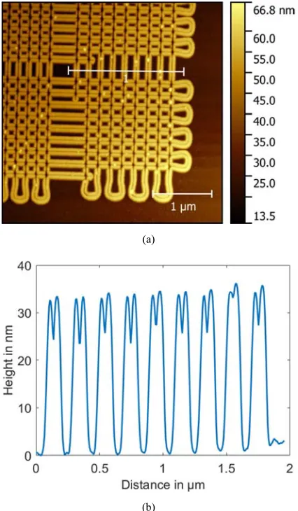
Figure 9. (a): AFM picture of intersected double line features written via SPL and etched at cryogenic temperatures into silicon. (b): Contour of the measured double line features was obtained at the section indicated by the white line in the AFM picture. The height of the features is about 30 nm after etching. The measured total width is 130 nm, whereas the distance between the two parallel lines is about 30 nm.
structures after etching is about 30 nm. The total width of these double lines is in the range of 130 nm, whereas the distance between the parallel lines is about 30 nm (etched trenches), resulting in a linewidth of a single line of about 50 nm. Line width and distance can be tuned by changing the FE-SPL exposure dose. The measured depth of such a trench is in the range of 5 nm (see Figure 9b), resulting in a discrepancy between total feature height (30 nm) and the measured trench depth (5 nm).
As can be seen from the SEM image of the generated double line features (Figure 10), the trench seems to be etched to the bottom. It can be concluded, that the measured trench depth of 5 nm is also just a measurement error due to the tip convolution in the AFM measurement.
As mentioned above, AFM pictures suffer from convolution of the real structure with the tip shape (tip radius around 10 nm). The result is an expanded measured structure. Furthermore, due to the tip size, it is also not able to fully penetrate into the etched trench between the two parallel lines. In this work no deconvolution was conducted, but there are different strategies to obtain the real feature after AFM [33- 35].
The double line features generated in this work could be used for pattern doubling, to further enhance the resolution capability of the lithography method. The use of the as produced double lines as spacer for “spacer defined double patterning” is another method to generate special nanostructures [36]. In Figure 11 the mechanism can be seen.
After Scanning Probe Lithography and wet development, nanoscale double line features are generated. Subsequently, a second layer can be deposited on top of the features. After an anisotropic etch step, followed by resist removal, dense, highly parallel features in the nano scale can be produced on top of the substrate. Afterwards these features can be used as base for future production steps.
Figure 10. SEM picture of the etched double line features. A fully etched trench between the two parallel lines can be seen.
Figure 11. Procedure to use double line features for spacer defined double patterning.
7. Conclusion
Here, a method to estimate the silicon-to-resist selectivity (plasma durability) of different types of resist was presented. As a result, the molecular glass resist calixarene has a selectivity of about 4:1 to silicon. The plasma durability of calixarene, AZ Barli, P3HT and PMMA is comparable. Since calixarene, P3HT and AZ Barli offer similar FE-SPL resolutions (10 nm half pitch), the best resist for generation of a certain type of nanostructure can be chosen according to
their individual properties as conductivity, tone switching and stiffness. Future high resolution lithography by FE-SPL and pattern transfer by cryogenic etching should be based on these resists. With an applied cryogenic etching step, field-emission scanning probe lithography offers a route for single nano-digit manufacturing and eventually could replace some cost-intensive lithography techniques in terms of resolution, patterning with low electron energy, direct patterning, tone switching, ambient conditions and costs.
parallel double line features in silicon by FE-SPL, wet development and cryogenic etching was demonstrated. These structures could be used for spacer defined double patterning in the future. Recently, single electron transistors were patterned on SOI-Wafer chips by FE-SPL, followed by a pattern transfer using cryogenic etching. The capability of these single electron transistors to work at room temperature was demonstrated [1]. Furthermore, we were able to generate templates with FE-SPL. These templates can be used for the production of high fidelity structures by nanoimprint lithography, enabling a high-throughput, high-resolution fabrication chain for future nanoelectronic devices like quantum dots and single electron devices [37].
Acknowledgments
The research leading to these results has received funding from the European Union’s Seventh Framework Programme FP7/2007-2013 under Grant Agreement No. 318804 (Single Nanometer Manufacturing for beyond CMOS devices – acronym: SNM).
The authors also gratefully acknowledge the support by the Deutsche Forschungsgemeinschaft (DFG) in the framework of Research Training Group “Tip- and laser-based 3D-Nanofabrication in extended macroscopic working areas” (GRK 2182) at the Technische Universität Ilmenau, Germany.
References
[1] I. W. Rangelow, A. Ahmad, T. Ivanov, M. Kaestner, Y. Krivoshapkina, T. Angelov, S. Lenk, C. Lenk, V. Ishchuk, M. Hofmann, D. Nechepurenko, I. Atanasov, B. Volland, E. Guliyev, Z. Durrani, M. Jones, C. Wang, D. Liu, A. Reum, M. Holz, N. Nikolov, W. Majstrzyk, T. Gotszalk, D. Staaks, S. Dallorto, and D. L. Olynick, “Pattern-generation and pattern- transfer for single-digit nano devices,” J. Vac. Sci. Technol. B, Nanotechnology and Microelectronics: Materials, Processing, Measurement, and Phenomena 34 (6), 06K202 (2016). [2] S. Lenk, M. Kaestner, C. Lenk, T. Angelov, Y. Krivoshapkina,
Ivo W. Rangelow, "2D Simulation of Fowler-Nordheim Electron Emission in Scanning Probe Lithography". J Nanomater Mol Nanotechnol 5 (6) (2016).
[3] I. W. Rangelow, Tz. Ivanov, Y. Sarov, A. Schuh, A. Frank, H. Hartmann, J.-P. Zöllner, D. Olynick, V. Kalchenko, "Nanoprobe maskless lithography.", Proc. SPIE 7637 (2010). [4] Z. Durrani, M. Jones, M. Kaestner, M. Hofer, E. Guliyev, A.
Ahmad, T. Ivanov, J.-P. Zoellner, Ivo W. Rangelow, "Scanning probe lithography approach for beyond CMOS devices," Proc. SPIE 8680, Alternative Lithographic Technologies V, 868017 (2013).
[5] I. W. Rangelow, “Scanning proximity probes for nanoscience and nanofabrication,” Microelectronic Engineering 83 (4-9), 1449–1455 (2006).
[6] K. Ivanova, Y. Sarov, T. Ivanov, A. Frank, J. Zöllner, C. Bitterlich, U. Wenzel, B. E. Volland, S. Klett, I. W. Rangelow, P. Zawierucha, M. Zielony, T. Gotszalk, D. Dontzov, W.
Schott, N. Nikolov, M. Zier, B. Schmidt, W. Engl, T. Sulzbach, and I. Kostic, “Scanning proximal probes for parallel imaging and lithography,” J. Vac. Sci. Technol. B 26 (6), 2367–2373 (2008).
[7] T. Ivanov, T. Gotszalk, T. Sulzbach, and I. W. Rangelow, “Quantum size aspects of the piezoresistive effect in ultra thin piezoresistors,” Ultramicroscopy 97 (1-4), 377–384 (2003). [8] T. Gotszalk, P. Grabiec, and I. W. Rangelow, “Piezoresistive
sensors for scanning probe microscopy,” Ultramicroscopy 82 (1-4), 39–48 (2000).
[9] M. Kaestner, T. Ivanov, A. Schuh, A. Ahmad, T. Angelov, Y. Krivoshapkina, M. Budden, M. Hofer, S. Lenk, J.-P. Zoellner, I. W. Rangelow, A. Reum, E. Guliyev, M. Holz, and N. Nikolov, “Scanning probes in nanostructure fabrication.”, Vac. Sci. Technol. B, Nanotechnology and Microelectronics: Materials, Processing, Measurement, and Phenomena 32 (6), 06F101 (2014).
[10] M. Kaestner, K. Nieradka, T. Ivanov, S. Lenk, Y. Krivoshapkina, A. Ahmad, T. Angelov, E. Guliyev, A. Reum, M. Budden, T. Hrasok, M. Hofer, C. Neuber, and I. W. Rangelow, “Electric field scanning probe lithography on molecular glass resists using self-actuating, self-sensing cantilever,” Proc. SPIE 90490C (2014).
[11] D. M. Eigler and E. K. Schweizer, “Positioning single atoms with a scanning tunnelling microscope,” Nature 344 (6266), 524–526 (1990).
[12] O. Custance, R. Perez, and S. Morita, “Atomic force microscopy as a tool for atom manipulation,” Nature nanotechnology 4 (12), 803–810 (2009).
[13] S. Tachi, K. Tsujimoto, and S. Okudaira, “Low‐temperature reactive ion etching and microwave plasma etching of silicon,” Appl. Phys. Lett. 52 (8), 616–618 (1988).
[14] E. S. Aydil, J. A. Gregus, and R. A. Gottscho, “Electron cyclotron resonance plasma reactor for cryogenic etching,” Review of Scientific Instruments 64 (12), 3572–3584 (1993). [15] G. S. Oehrlein and Y. Kurogi, “Sidewall surface chemistry in
directional etching processes,” Materials Science and Engineering: R: Reports 24 (4), 153–183 (1998).
[16] S. Aachboun and P. Ranson, “Deep anisotropic etching of silicon.”, Vac. Sci. Technol. A: Vacuum, Surfaces, and Films 17 (4), 2270–2273 (1999).
[17] S. Tachi, K. Tsujimoto, S. Arai, and T. Kure, “Low‐ temperature dry etching.”, Vac. Sci. Technol. A: Vacuum, Surfaces, and Films 9 (3), 796–803 (1991).
[18] I. W. Rangelow, “Critical tasks in high aspect ratio silicon dry etching for microelectromechanical systems.”, Vac. Sci. Technol. A: Vacuum, Surfaces, and Films 21 (4), 1550–1562 (2003).
[19] C. B. Mullins and J. W. Coburn, “Ion‐beam‐assisted etching of Si with fluorine at low temperatures,” Journal of Applied Physics 76 (11), 7562–7566 (1994).
[21] J. W. Bartha, J. Greschner, M. Puech, and P. Maquin, “Low temperature etching of Si in high density plasma using SF6/O2,” Microelectronic Engineering 27 (1-4), 453–456
(1995).
[22] I. W. Rangelow, “Reactive ion etching for microelectrical mechanical system fabrication,” J. Vac. Sci. Technol. B 13 (6), 2394 (1995).
[23] D. L. Olynick, J. A. Liddle, B. D. Harteneck, S. Cabrini, and I. W. Rangelow, “Nanoscale pattern transfer for templates, NEMS, and nano-optics,” in, edited by M.-A. Maher, H. D. Stewart, J.-C. Chiao, T. J. Suleski, E. G. Johnson, and G. P. Nordin (SPIE, 2007), 64620J.
[24] X. Mellhaoui, R. Dussart, T. Tillocher, P. Lefaucheux, P. Ranson, M. Boufnichel, and L. J. Overzet, “SiOxFy passivation layer in silicon cryoetching,” Journal of Applied Physics 98 (10), 104901 (2005).
[25] T. Tillocher, R. Dussart, L. J. Overzet, X. Mellhaoui, P. Lefaucheux, M. Boufnichel, and P. Ranson, “Two Cryogenic Processes Involving SF6, O2, and SiF4 for Silicon Deep
Etching,” J. Electrochem. Soc. 155 (3), D187 (2008).
[26] A. F. Isakovic, K. Evans-Lutterodt, D. Elliott, A. Stein, and J. B. Warren, “Cyclic, cryogenic, highly anisotropic plasma etching of silicon using SF6/O2,” Journal of Vacuum Science
& Technology A: Vacuum, Surfaces, and Films 26 (5), 1182– 1187 (2008).
[27] R. Kassing and I. W. Rangelow, “Etching processes for High Aspect Ratio Micro Systems Technology (HARMST),” Microsystem Technologies 3 (1), 20–27 (1996).
[28] J. Fujita, “Nanometer-scale resolution of calixarene negative resist in electron beam lithography,” J. Vac. Sci. Technol. B 14 (6), 4272 (1996).
[29] M. J. Rooks and A. Aviram, “Application of 4-methyl-1-acetoxycalix [6] arene resist to complementary metal–oxide– semiconductor gate processing,” J. Vac. Sci. Technol. B 17 (6), 3394 (1999).
[30] Y. Ohnishi, J. Fujita, Y. Ochiai, and S. Matsui, “Calixarenes-prospective materials for nanofabrications-,” Microelectronic Engineering 35 (1-4), 117–120 (1997).
[31] Y. Krivoshapkina, M. Kaestner, C. Lenk, S. Lenk, and I. W. Rangelow, “Low-energy electron exposure of ultrathin polymer films with scanning probe lithography,” Microelectronic Engineering 177, 78–86 (2017).
[32] L. Janasz, D. Chlebosz, M. Gradzka, W. Zajaczkowski, T. Marszalek, K. Müllen, J. Ulanski, A. Kiersnowski, and W. Pisula, “Improved charge carrier transport in ultrathin poly (3-hexylthiophene) films via solution aggregation,” J. Mater. Chem. C 4 (48), 11488–11498 (2016).
[33] J. Canet-Ferrer, E. Coronado, A. Forment-Aliaga, and E. Pinilla-Cienfuegos, “Correction of the tip convolution effects in the imaging of nanostructures studied through scanning force microscopy,” Nanotechnology 25 (39), 395703 (2014). [34] S. Yuan, F. Luan, X. Song, L. Liu, and J. Liu, “Reconstruction
of an AFM image based on estimation of the tip shape,” Meas. Sci. Technol. 24 (10), 105404 (2013).
[35] A. T. Winzer, C. Kraft, S. Bhushan, V. Stepanenko, and I. Tessmer, “Correcting for AFM tip induced topography convolutions in protein-DNA samples,” Ultramicroscopy 121, 8–15 (2012).
[36] A. J. M. Mackus, A. A. Bol, and W. M. M. Kessels, “The use of atomic layer deposition in advanced nanopatterning,” Nanoscale 6 (19), 10941–10960 (2014).
![Figure 1. (a) SEM image of the thermomechanically actuated piezoresistive cantilever. (b) A sub-10nm write and imaging resolution by SPL/AFM require cantilever tips with radius of curvature of < 15 nm [5]](https://thumb-us.123doks.com/thumbv2/123dok_us/961990.1595514/2.595.47.285.417.731/figure-thermomechanically-actuated-piezoresistive-cantilever-resolution-cantilever-curvature.webp)
![Figure 2. Concept of closed-loop for imaging and patterning. Figure according to [4].](https://thumb-us.123doks.com/thumbv2/123dok_us/961990.1595514/3.595.83.533.85.433/figure-concept-closed-loop-imaging-patterning-figure-according.webp)
![Figure 5. The most significant aspect ratio dependent effects. Figure according to [18]](https://thumb-us.123doks.com/thumbv2/123dok_us/961990.1595514/5.595.44.290.542.625/figure-significant-aspect-ratio-dependent-effects-figure-according.webp)