A Comparative Study on Single Switch and
Quadratic Buck-Boost Converters
1
Febi Thomas V1, Ninu Joy2, Kiran Boby3
1
PG Student, 2,3Professor
Department of Electrical & Electronics Engineering
Mar Athanasius College of Engineering, Kothamangalam, Kerala, India
Abstract-Conventional voltage regulators are less capable of providing high voltage gain in an efficient manner for applications demanding steady dc voltage. The switching frequency of the power converter must be increased in order to achieve small size, light weight, and low noise. Many new converters which are modifications of the conventional voltage regulators are being proposed inorder to improve the converter performance characteristics. A comparative study on such converters are helpful in selecting the most suitable converter for a particular application. Here, the converters taken for comparison are quadratic buck-boost converter and single switch buck-buck-boost converter. Both the converters are individual based on ripple factor, power density, and output voltage with same switching frequency, duty ratio and input voltage. The simulation of both the converters were performed using MATLAB/Simulink. The variation of output voltage with respect to duty ratio and output ripple with respect to switching frequency of both converters were tabulated and plotted. The prototype of 20kHz, 5W of single switch buck-boost converter was implemented using PIC16F877A microcontroller and the simulation results were compared.
Keyword- Single Switch Buck-Boost Converter, Quadratic Buck-Boost Converter, Voltage gain,
Switch Stress.
I. INTRODUCTION
In recent years, the usage of renewable energy systems such as fuel cell and photovoltaic systems are encouraged due to various environmental troubles caused by other fuels, such as climate change and global warming by increased emissions of carbon dioxide. With increasing attention to environmental problems, energy achieved from the fuel cell systems is focused on the low environmental effects and clean energy. Fuel cells are an effective alternative to replace fuels in emergency power systems and vehicles. Fuel cells can be used as clean energy by users with low emissions of carbon dioxide. Due to steady operation with renewable fuel supply and high effectiveness and effciency, the fuel cell has been recognized increasingly as a suitable alternative source. There are some problems of this fuel such as high cost, but
and small size. The output voltage of the fuel cell unit is low and is not steady and it cannot be directly connected to the load. For applications that need a steady DC voltage, buck-boost DC-DC converter is required so as to obtain an incremented or decremented voltage at the output compared to the input.
However, the traditional buck-boost converter is not suitable for fuel cell sources. The traditional buck-boost converter efficiency is expected high, however, it is low and is limited by the effects of diodes, switches and equivalent series resistance (ESR) of capacitors and inductors. In order to obtain the high efficiency and high voltage gain, many converters, which are modifications of conventional buck-boost converters have been suggested by various researchers inorder to attain more and more efficient converters with low cost. A multiwinding coupled inductor and a voltage doubler can be used to achieve high step-up voltage gain [1]. But the leakage inductance of the coupled inductor is so important that it cause high voltage spikes and adds the voltage stress. Also, the voltage spike of the main switch is limited and voltage stress can be adjusted by the turns ratio of the coupled-inductor. Converter with switched capacitor techniques with capacitors on the output-stacking which are charged in parallel and discharged in series are also employed to achieve high step-up gain [2].
II. SINGLESWITCHANDQUADRATIC BUCK-BOOSTCONVERTERS
Here, Single switch buck-boost converter and quadratic buck-boost converter are compared based on various factors.
Single Switch Buck-Boost Converter
Fig.1: Circuit diagram of single switch buck- boost converter
Principle of Operation
This converter consists of one power switch S, three diodes D1, D2, D3, three inductors L1, L2, L3, ve
capacitors C1, C2, C3, C4, Co and load R. Certain
assumptions are taken for the analysis of this circuit. The capacitors in this converter are large
enough, hence the voltage across capacitors are assumed to be constant.
The main switch of the converter is treated as ideal and the parasitic capacitor of the main switch is neglected.
There are two modes of operation for this converter in continuous conduction mode(CCM). The duty ratio can be varied so as to obtain the required voltage gain and output voltage. The input current of the converter is discontinuous. Here, the input current and the switch current are the same. The output voltage of the converter is negative as in a conventional buck-boost converter. This converter operates as a universal power supply and it is appropriate for low voltage and low power applications.
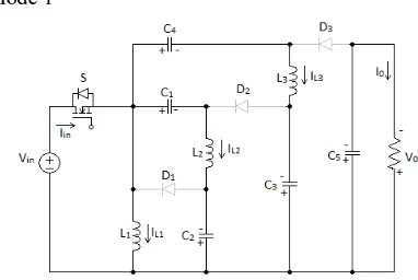
Mode 1
Fig.2 Equivalent Circuit during Mode 1.
During mode 1, the switch S is turned on and the diodes D1, D2 and D3 are turned off. The
inductors L1, L2 and L3 are magnetized linearly. The
capacitors C1 and C4 are charged by the capacitors
C2 and C3.
Fig. 3: Waveforms (Mode 1 shaded) Mode 2
Fig. 4: Equivalent circuit during Mode 2
During mode 2, the switch S is turned off and the diodes D1, D2 and D3 are turned on. The inductors L1,
L2 and L3 are demagnetized linearly. The capacitor
C2 is charged by the inductor L1 and the capacitor C3
is charged by the inductors L1 and L2 and the
capacitors C1 and C4 are discharged.
VL1 = Vi (1)
VL2 = VC2 ˗VC1+Vi (2)
VL3= VC3˗VC4 + Vi (3)
VL1 = ˗VC2 (4)
VL2 = VC2 ˗ VC3 (5)
.
Fig. 5: Waveforms (Mode 2 shaded)
By applying volt-sec balance principle on inductors L1, L2 and L3, we can obtain the voltage transfer
ratio in CCM as:
(7)
A. Quadratic Buck-Boost Converter
Fig. 6: Circuit diagram of quadratic buck-boost converter
Principle of Operation
It consists of two diodes, D2, two inductors L1, L2,
two capacitors C1, C2 and two switches S1 , S2. The
two switches in the circuit are turned on simultaneously so that there is no phase delay between them. There are two modes of operation for this circuit.
The inductors acts as the medium for storing and transferring energy. By applying volt-sec balance principle,
(8)
Mode 1
Fig. 7: Equivalent Circuit during mode 1
In this mode, S1 and S2 are turned on
simultaneously which makes D1 and D2 be reversely
biased. L1 stores the energy by the input voltage
source. L2, stores the energy while C1 is being
discharged and C2 is supplying the load.
Mode 2
Fig. 8: Equivalent Circuit during mode 2
In this mode, S1 and S2 are turned off
simultaneously. The diodes D1 and D2 are forward
biased. The inductors L1 and L2 transfers the energy
stored in them during this interval thereby charging C1 and C2 respectively
.
VL1 = VC1 (11)
VL2=V0 (12)
VL1 = Vin (9)
VL2 = VC1 (10)
D
1
D
3
V
V
i O
2 2
i O
D)
(1
D
V
V
III. SIMULATIONMODELSANDRESULTS The simulation of single switch buck-boost converter is performed in MATLAB/Simulink 2014. The detailed simulink model is shown in figure 9.
Simulation Parameters of Single Switch Buck-Boost Converter are given in table 1.
Table 1: Simulation Parameters of Single Switch Buck-Boost Converter
Fig. 9: Simulink Model of Single Switch Buck-Boost Converter
Simulation is performed with 11 V input DC source and a 100Ω resistive load. The current through inductors and voltage across capacitors are measured.
Simulation Results of Single Switch Buck-Boost Converter are shown below:
Fig. 10. (a)gate pulse (b)voltage across switch in buck operation.
Fig. 11. (a)input voltage (b)output voltage in buck operation.
Fig. 12. (a)input current (b)output current in buck operation.
Fig. 13: Current through (a)L1, (b)L2, (c)L3 in
buck operation
Fig. 15. (a)gate pulse (b)voltage across switch in boost operation
Fig. 16. (a)input voltage (b)output voltage in boost operation
Fig. 17. (a)input current (b)output current in boost operation.
Fig. 18: Current through (a)L1, (b)L2, (c)L3 in
boost operation
Fig.19 :Voltage across (a)C1, (b)C2, (c)C3, (c)C4,
(d)C5 in boost operation
Simulation Parameters of quadratic buck-boost converter are shown in table 2.
Table 2: Simulation Parameters of Quadratic Buck-Boost Converter
Fig. 20: Simulink Model of Quadratic Buck-Boost Converter
Simulation results of quadratic buck-boost converter are shown below:
Fig.21: (a)Input Voltage, (b)Output Voltage in buck operation
Fig.22: (a)Input current, (b)current through L2,
(c)Output Current in buck operation
Fig.23: (a)Input Voltage, (b)Output Voltage in boost operation
Fig.24: (a)Input current, (b)current through L2,
(c)Output Current in boost operation
IV. COMPARISON OF SINGLE SWITCH AND QUADRATIC CONVERTERS
Table 3 : Comparison of various parameters
Fig:25 Output voltage v/s duty ratio of both converters
Fig:26 Output ripple v/s frequency of both converters
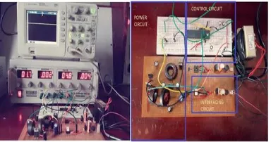
Fig.27: Experimental Setup
A prototype of 20kHz, 5W of single switch buck-boost converter was setup in lab. The output voltage waveforms in both buck and boost mode operations were observed in digital storage oscilloscope(DSO).
Fig. 28: Gate pulse and output voltage in buck operation
Fig.29: Gate pulse and output voltage in boost operation
VI. CONCLUSIONS
The single switch buck-boost converter and quadratic buck boost converters are essentially the modifications of conventional buck-boost converter with improved performance characteristics. Both these converters were compared on the basis of parameters like switching stress, number of components and graphs were plotted for output volt-age with respect to duty ratio and output voltvolt-age ripple with respect to switching frequency. The single switch buck-boost converter gives better performance than the quadratic buck boost converter in the way of less ripple voltage and high output voltage in the range of operating duty ratio and frequency. For a switching frequency of 37kHz and 0.58 duty ratio, the quadratic buck-boost converter
provides only 20 V as output whereas single switch converter provides an output voltage of magnitude 42 V for the same input voltage of 11 V. The control circuit for single switch converter is simple since there is only one switch. But the complexity of single switch converter is slightly more due to the presence of more number of components. A 20kHz, 5W prototype of single switch buck-boost converter was implemented using PIC16F877A microcontroller. For an input voltage of 11 V, about 2 V was obtained in buck operation and for an input voltage of 2.7 V, an output voltage of 11 V was obtained in boost operation and these results were matching the results obtained from the simulation of prototype of the converter.
REFERENCES
[1] S.K.Changchien, T.J.Liang, J.F.Chen and L.S.Yang,
“Novel high step-up DC-DC converter for fuel cell energy conversion system", IEEE Transactions on Industrial Electronics, Vol.57, No:6, June 2010.
[2] Y. P. Hsieh, J. F. Chen, T. J. Liang and L. S. Yang, “Novel high stepup DC-DC converter with coupled-inductor and switched-capacitor techniques", IEEE Transactions on Industrial Electronics, Vol.59, No:2, February 2012.
[3] T. J. Liang, J. H. Lee, S. M. Chen, J. F. Chen, L. S. Yang, “Novel Isolated High-Step-Up DC-DC Converter With voltage lift” IEEE Transactions on Industrial Electronics, Vol.60, No:4, April 2013.
[4] L. S. Yang, T. J. Liang and J. F. Chen, “Transformer-less
DC-DC converter with high voltage gain", IEEE Transactions on Power Electronics, Vol 56, No:8, August 2009
[5] C. T. Pan, C. F. Chuang and C. C. Chu, “A novel
transformer less interleaved high step-down conversion ratio DC-DC Converter with low switch voltage stress", IEEE Transactions on Power Electronics, Vol.61, No:10, October 2014
[6] Ned Mohan, Undeland and Robbin, “Power Electronics:
converters, Appli-cation and design”, John Wiley and sons.Inc, Newyork, 1995.
[7] O. Abutbul, A. Gherlitz, Y. Berkovich and A. Ioinovici,
“Step-up switching-mode converter with high voltage gain using a switched capacitor circuit.” IEEE Trans. Circuits Syst. I, vol. 50, no. 8, pp.1098-1102, Aug. 2003.
[8] K. I. Hwu and W.Z. Jiang, “Isolated step-up converter
based on flyback converter and charge pumps,” IET Power
Electron., vol. 7, no.9, pp. 2250–2257, Sep. 2014.
[9] C. T. Pan, C. F. Chuang and C. C. Chu, “A novel
transformer less interleaved high step-down conversion ratio DC-DC converter with low switch voltage stress”,
IEEE Trans. Ind. Electron., vol. 61 , no. 10, pp. 5290 -5299 , Oct. 2014.
[10] L. S. Yang, T. J. Liang, and J. F. Chen, “Transformer-less
DC–DC converter with high voltage gain,” IEEE Trans.