Latch-Type Sense Amplifier Modification for
Coupling Suppression
Chandra kishore*1, Amit Kumar#2, 1
Department of Electronics Engineering, Institute of Engineering and Technology, Sitapur Road, Aliganj, Lucknow, India
2
Department of Electronics Engineering, Institute of Engineering and Technology, Sitapur Road, Aliganj, Lucknow, India
Abstract
When continuously increase the semiconductor fabrication technology, then continually shrink the channel length and pitch of the CMOS device with the vigorous process variation and signal coupling effect. Here explained how the action of sense amplifier disturbed by the property of coupling effect. In this paper, we design the single stage amplifier, modified single stage amplifier and multistage amplifier. The operational amplifier contains the high gain, high input impedance and low output impedance. The circuits are simulated by using the .25µm CMOS technology. All results obtained by using the tanner tool version 13.0 software. The comparison among all amplifiers parameters like as power dissipation, leakage voltage and supply voltage of the circuit.
Keywords Operational Amplifier (OP-AMP), CMOS,
Metal oxide semiconductor (MOS)
I. INTRODUCTION
It is essential for all memories as that dynamic random access memory (DRAM) and static random access memory (SRAM) for any read, write operations. It shows the comparison between bit line voltage and rail to rail complemented output voltage. It sense mainly write operation [1]. It is a peripheral circuit which are exist in each and every column of memory array. It detects the correct signal when the input difference voltage of the sense amplifier is larger than off-set voltage of the sense amplifier and amplifier gives the correct logic levels. Ideally the off-set voltage of any sense amplifier is approximately zero but practically it is not possible because due to the devices or transistors mismatching [4]. When the off-set voltage of sense amplifier is approximately zero then the sense amplifier sense the correct voltage which are present in the input bit lines whenever the differential bit line voltage does not zero.
We discuss the when introducing the coupling capacitance in sense amplifier then the sense amplifier how to act due to the coupling effect [2]. Here we control the time by using the output waveform’s transient and Fourier analysis. We can achieve the enhancement CMOS structure under the differential input in our tanner tool spice design and this can implemented by the use of .25 um CMOS technology. The sense amplifier’s basic process is to sense the
differential input voltage and to reduce the dynamic dissipated power and access time of sense amplifier [5]. This is more capable to differential noises and offset voltages and by using the output waveform we check the coupling effect in sense amplifier when comparison with the old CMOS design.
In analog electronics the most important and useful component is operational amplifier. The operational amplifier used most widely in electronics but it contains some limitation which performance depends upon operating frequency which is not exceeding the 1Mz. Some models have been designed for higher operating frequency [10].
II. PREVIOUSWORK
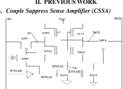
A. Couple Suppress Sense Amplifier (CSSA)
Figure 1: CMOS Representation of CSSA
devices which causes very less increment in the area of the devices.
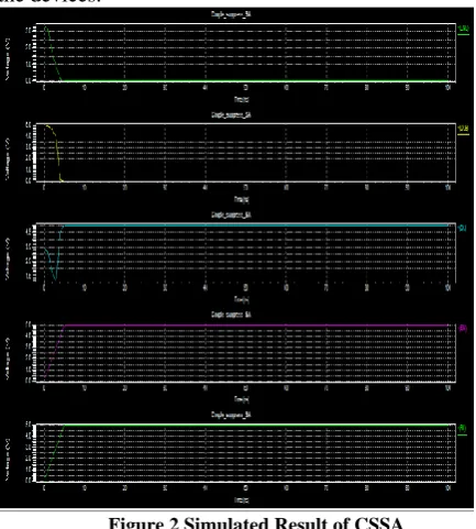
Figure 2 Simulated Result of CSSA
III.OURPROPOSEDWORK
The enhancement CMOS design brings more difficulties, which is specially say that for SRAM, that is the unfavourable memory block of SoC. In this paper we present the design procedure of single stage operational amplifier and multistage operational amplifier. In this paper we have simulated the diode connected load with two extra PMOS which get the better trade-off among the output swing voltage, voltage gain and the common mode range. The properties of operational amplifier are high input impedance, low output impedance and it also contains the high gain. We take the dimension of transistors with width W = 2.5µm and length L = 0.25µm. Here we have used the 0.25µm CMOS technology.
A. CMOS Representation Of Single Stage Amplifier
Figure 2 Single Stage Amplifier
The measurement of single ended signal with respect to the ground where as the differential signal measured with respect to the two nodes usually both nodes contains the equal and opposite in amplitude. The important advantages of differential signal over the single ended signal which protecting from environmental noise. The single stage amplifier contains the four transistors like as NMOS1, NMOS2 and PMOS1, PMOS2. In this circuit the two NMOS transistors connected back to back though the gate of NMOS and the NMOS1 and PMOS1 both sources are connected to the common gate of NMOS1 and NMOS2. The output of this amplifier is connected to the source of NMOS2 and PMOS2. At the output terminal one load capacitance is connected which value is 1PF. At the PMOS transistors both differential inputs are connected i.e. at the PMOS1 terminals the input signals are apply and at the PMOS2 terminals the clock pulse is applied. The power supply VDD is applied at the drain
of the both NMOS transistors (VDD = 5V).
B. Modified Single Stage Amplifier
In the modified single stage amplifier the three extra transistors are added i.e. two NMOS and one PMOS. In the NMOS transistors there are two signals are apply in one terminal the input pulse and in the other terminal the read signals are applied. In the PMOS transistors i.e. PMOS1 contain one terminal that is known as input terminal (In) and PMOS2 terminal known as write terminal (ww1) and PMOS3 transistor contain the clock terminal (clk). This circuit contains the four NMOS transistors. The two transistors NMOS1 and NMOS2 contains two terminals which is known as In-1 and rw1 and take the output in between source terminals of NMOS1, NMOS2 and PMOS1.
C. Proposed Circuit Diagram of Two Stage Amplifier
Figure 4 Multistage Amplifier
This is the cascade of two stages, the first stage provides the high gain and second stage provides the large output swing. This circuit contains the 8 transistors and one current source (I = 5 micrometer). These 8 transistors name as 4 PMOS transistors and 4NMOS transistors. The input terminal is common for both NMOS1 and NMOS2 gate terminal and inputs I/P and clock pulse provided through the PMOS1 and the PMOS2 transistors. The PMOS transistors PMOS3 and PMOS4 are connected back to back through gate terminals.
The circuit is simulated by using the tanner 13 version software and the output waveform find using this tool and also calculate the dissipated power for each proposed circuit. Take the dimension of each transistors is length L = .25 micrometer and width of each transistors is W = 2.5 micrometer. In this circuit the output is taken in between PMOS3 and NMOS3 source terminals.
III. SIMULATEDRESULT
A. Schematic Diagram of Single Stage Amplifier
Figure 5 Schematic Diagram of III (A)
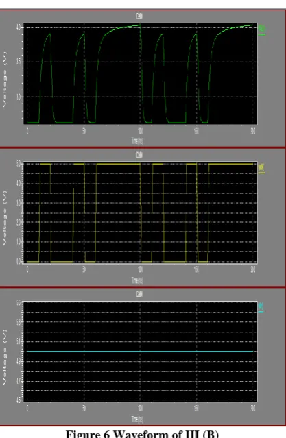
B. Output Waveform of Single Stage Amplifier
Figure 6 Waveform of III (B)
In this circuit we take a clock pulse which value is 0100101111 (bit value) and input is 5v and output waveform show the amplified charging and discharging due to the capacitance at the output node.
C. Modified Single Stage Amplifier
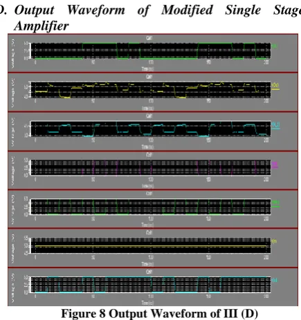
D. Output Waveform of Modified Single Stage Amplifier
Figure 8 Output Waveform of III (D)
This output waveform show the read and write operation when we apply the input In = 5.0v and clock (0000111010) and In1 = 01000101111. The read operation bit contain rw1 = 1111010110 and write operation contain the bit ww1 = 1010101011 then during this the output voltage amplified and during amplifying some distortion exist in the output and due to this the leakage voltage exist and also reduce the power dissipation.
E. Schematic of Two-Stage Amplifier
Figure 9 Schematic of III (E)
F. Output Waveform of Two-Stage Amplifier
Figure 10 Output Waveform of III (F)
In two stage, the output waveform show the amplified output voltage during this some distortion exist which is 1.6v. In this the input bit is 0100101111 and clock pulse is 0100101111 and input voltage is 5.0v.
IV.COMARISONTABLE
Single stage amplifier Modified single stage amplifier Two stage amplifi er Supply voltage
5.0V 5.0V 5.0V
Output voltage
4.3V 4.6V 3.4V
Leakage voltage
0.7V 0.4V 1.6V
Power dissipation 1.707×10^-3 Watts 2.457×10^-7 Watts 2.237× 10^-13 Watts technology 0.25µm 0.25µm 0.25µm
V. CONCLUSION
Various types of operational amplifier were designed and these implemented circuits which are single stage amplifier, modified single stage amplifier and two stage amplifier simulated by the tanner simulated tool by using the .25µm CMOS technology. The OP-AMP show the leakage voltage, power dissipation, input voltage and output voltage.
ACKNOWLEDGEMENT
I would like to convey my most sincere thanks to my guide Assistant Prof. Amit Kumar under whose supervision and precious guidance I could complete this work on time. I could not have imagined having a better advisor and mentor for my thesis work.
I extended my sincere thanks to Dr. Subodh Wairya, Head of Electronics Engineering Department, for their sincere cooperation and motivation. I am very thankful to Prof. S.R.P. Sinha for their invaluable guidance and continuous encouragement during the entire period of research work.
I also would like to thanks to Dr. Rajiv Kumar Singh of Electronics Engineering Department for their motivation and cooperation in my work to be completed for entire period of working.
REFERENCES
[1] R.Singh and N. Bhat, “An offset compensation technique for
latch type sense amplifiers in high-speed low-power SRAMs,” IEEE Trans. Very Large Scale Integr. (VLSI) Syst., vol. 12, no. 6, pp. 652–657, Jun. 2004.
[2] B.Wicht, T. Nirschl, and D. Schmitt-Landsiedel, “Yield and
speed optimization of a latch-type voltage sense amplifier,” IEEE J. Solid-State Circuits, vol. 39, no. 7, pp. 1148–1158, Jul. 2004.
[3] A.-T.Do, Z.-H. Kong, and K.-S. Yeo, “Criterion to evaluate
[4] S.J.Lovett, G. A. Gibbs, and A. Pancholy, “Yield and matching implications for static RAM memory array sense-amplifier design,” IEEE J. Solid-State Circuits, vol. 35, no. 8, pp. 1200– 1203, Aug. 2000.
[5] J.S.Shah, D. Nairn, and M. Sachdev, “An energy-efficient
offsetcancelling sense amplifier,” IEEE Trans. Circuits Syst., vol. 60, no. 8, pp. 477–481, Aug. 2013.
[6] A.K.Gundu, W. Singh, and S. M. Divi, “A proposed low-offset
sense amplifier for SRAM applications,” in Proc. 2nd Int. Conf. Signal Process. Integr. Netw. (SPIN), 2015, pp. 965–967.
[7] B.S.Amrutur and M. A. Horowitz, “A replica technique for
wordline and sense control in low-power SRAM’s,” IEEE J. Solid-State Circuits, vol. 33, no. 8, pp. 1208–1219, Aug. 1998.
[8] HSPICE User Guide: Simulation and Analysis? Version
D-2010.03-SP1, Synopsys, Inc. Mountain View, CA, USA, Jun. 2010.
[9] Luca Bettini ETZ J93, Petrit Bunjaku ETZ J64.2, “Analog
Integated Circuits Design of a Single Stage OP-AMP,”
[10] Ramakant a. Gayakwad Mt. Slierra collage, “OP-AMP and