e
-ISSN: 2250-3021,
p
-ISSN: 2278-8719
Vol. 3, Issue 1 (Jan. 2013), ||V5|| PP 14-22
Power Optimized Divide-By-2/3 Counter Based Clock Design
Using Multiplexer
Anandkumar.M
1, Prabhakaran.G
2, Dr.Marimuthu.C.N
31PG Scholar, 2Assistant Professor, 3Professor 1II-M.E (VLSI DESIGN) Nandha Engg College, Erode
2,3
Department of ECE Nandha Engg College, Erode
Abstract: This paper proposes a advanced method of extended true-single-phase-clock (E-TSPC) based
divide-by-2/3 counter design for providing low supply voltage and low power consumption. The counting logic and the mode selection control can be desingned by the help of single transistor using wired OR method. The proposed method mainly focus on for saving power consumption and it reduces the critical path between the E-TSPC flip flops (FFs) for improving the operating frequency of the counter. E-TSPC will reduce the design time, Layout area, in power-delay-product and increase the operation speed can be achieved by the proposed design and expected 1.0 to 2.0% of power reduction. The E-TSPC Prescaler is implemented in low-power high-resolution frequency dividers for wireless local area network applications.
Index Terms: Extended true-single-phase-clock flip flops (E-TSPC FF), Transistor, low power, low voltage,
prescaler.
I.
INTRODUCTION
The counter is mainly used for counting number of clock cycles. In this paper we focus high speed by-N/N+1 counter (also called prescaler) is a fundamental module for frequency synthesizers. A divide-by- counter consists of flip-flops (FF) and extra logic, which determines the terminal count and it operates at a higher frequency and consumes higher power Consumption. FF based divide-by –N/N+1 designs adopt dynamic logic FFs such as single-phase clock (TSPC). The designs can be further enhanced by using extended true-single-phase-clock (E-TSPC) FFs for high speed and low power applications. E-TSPC designs remove the transistor stacked structure so that all the transistors are free of the body effect. They are thus more sustainable for high operating frequency operations in the face of low voltage supply.
II.
EXISTING SYSTEM
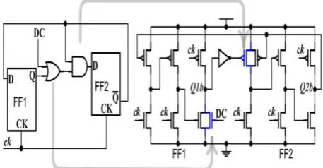
Past optimization efforts on prescaler designs focused on simplifying the logic part to reduce the circuit complexity and the critical path delay. For example, an E-TSPC design embedded with one extra PMOS/NMOS transistor can form an integrated function of FF and AND/OR logic . Moving part of the control logic to the first FF to reduce unnecessary FF toggling yields another version of prescaler design. These two classic designs each contains 16 transistors only and the mode control logic uses as few as 4 transistors. To achieve such circuit simplicity, it calls for a ratioed structure in the FF design. Despite its distinct speed performance, the incurred static and short circuit power consumptions are significant. Latest designs presented in A state-of-the-art divide by-2/3 counter design is given in Fig.1.
Fig 1: Previous E-TSPC-based divide-by-2/3 counter designs –design
somehow, the circuit enters this state, the next state will go back to a valid state 11, automatically. When DC is “1”,the output of FF1 will be disabled and FF2 alone performs the divide-by-2 function. Since the input to FF1 is not disabled, FF1 toggles as usual and causes redundant power consumption in the divide-by-2 mode operation in fig.2. This is because the pull up path is turned on all the time and the short circuit current is drawn repetitively whenever the clock signal turns “1”. The critical path delay, formed by the two FFs and the control logic, is the dominant factor of the prescaler’s maximum operating frequency.
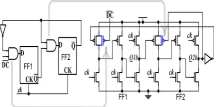
Fig 2: Previous E-TSPC-based divide-by-2/3 counter designs-design
In spite of the circuit simplicity in designs the inverter between FF1 and FF2, which is essential to the logic of divide-by-3, causes extra delay. Merging control logic with FF designs also introduces parallel connected transistors leading to larger parasitic capacitance adverse to both speed and power consumption. In view of these issues, our approach is keeping the circuit simplicity so that the delay and the power consumption problems can be improved at a time. The inverter between FF1 and FF2, which is essential to the logic of divide-by-3, causes extra delay. Merging control logic with FF designs also introduces parallel connected transistors leading to larger parasitic capacitance adverse to both speed and power consumption.
III.
PROPOSED SYSTEM
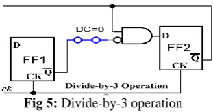
The logic structure of the proposed design is shown in Fig.3. The two FFs and the AND gate are common in previous designs. The OR gate for the divide control is replaced with a switch. Note that there is a negation bubble at one of the AND gate’s input. The output of FF1 is thus complemented before being fed to FF2. When the switch is open, the input from FF1 is disconnected and FF2 alone divides the clock frequency by 2 in fig.4.When the switch is close, FF1 and FF2 are linked to form a counter with three distinct states in fig.5. According to the simulation results given, E-TSPC design shows the best speed performance in various counter designs including the one using conventional transmission gate FFs. Besides the speed advantage, E-TSPC FFs are particularly useful for low voltage operations because of the minimum height in transistor stacking. Other than the two E-TSPC FFs, only one PMOS transistor is needed. The PMOS transistor controlled by the divide control signal serves as the switch. The AND gate plus its input inverter are achieved by way of wired-AND logic using no extra transistors at all. The proposed design scheme is far more sophisticated than the measure of simply adding one pass transistor may suggest.
Fig 3: Logic structure of proposed 2/3 counter design
applying Demorgan’s law to the Boolean equation gives rise to , which is exactly the desired logic. Since is applied to the input of , the inverter needed to complement the signal can be eliminated.
Fig 4: Divide-by-2 operation
Before elaborating on the functional correctness of this wired OR logic, the working principle of the E-TSPC FF design is briefly reviewed consists of two pseudo.PMOS inverters followed by a D-latch. When clock signal equals to 1, the outputs of the two inverters are pre-discharged to zero.
In the mean time, the PMOS and NMOS transistors of the D-latch (the third inverter) are both turned off so that the output value holds via the parasitic capacitance. When clock signal turns to 0, the first two inverters enter the evaluation phase and the D-latch becomes a pseudo NMOS inverter to admit the evaluation result from the preceding inverter. The wired-OR function is implemented by connecting the output node of FF1 and the output node of the 1st stage inverter in FF2 through a PMOS transistor. Any signal inconsistence between these two nodes must be resolved by way of logic OR. In other words, signal “1” must override signal “0”. In Table I, there exist two cases of such signal inconsistence. Case 1 occurs when both and are equal to “1”.When , node is both driven low by a pull down NMOS transistor N2 and pulled high by through PMOS transistor. Note that is actually a weak “1” retaining its level via parasitic capacitance.
Fig 5: Divide-by-3 operation
Although signal “0” seems to override signal “1”, this will not affect the correct value, i.e., “1”, to be latched in the evaluation phase. First, even though Q1b is vulnerable to the discharge by transistor N2, actually a weak “0” and will not affect the rising of node D2b. In particular, transistor P2 charges through transistor as well, which coincides with the next state we can see a steep 0 to 1 transition of due to this effect. This enhances the prescaler’s working frequency. A minimum channel length, which is 0.18 m, is adopted in all transistor designs. Although deliberate transistor sizing is required to ensure the functionalities of wired-OR and E-TSPC, both FFs share identical sizes to reduce the discharge hazard is alleviated by the threshold voltage drop across pMOS transistor .In particular, for low operations, the threshold voltage, enlarged further by the body effect, can well exceed one half. This can be shown in Fig.6. that the level degradation of is mild. Second, when the FF enters the evaluation phase, the pull down transistor N2 is cut off while transistor P1 is turned on and charges through transistor. The voltage level is raised up to 210 mV only. Although enlarging transistor P1 can boost the level and it will degrade the speed performance as well due to a larger capacitive load. Via proper transistor size tweaking in the following stages, this level is good enough for a correct “1” to be latched at when turns “1” again. A close exam at the waveform of node reveals that, in spite of a signal level over one half of it is not high enough to drive the output node to an erroneous state “0”. The second case of signal inconsistence occurs when both and are equal to “0”. In the hold phase node is always pulled low by transistor N2. In the evaluation phase, transistor N2 is turned off and node is pulled high via transistor P2.Although node keeps a contradictory signal “0”, it is design complexity. Besides the fixed-modulus dividers, dual-modulus counters can also be synthesized in a similar way by using more than one TSPC DFFs and additional feedback logic gates. The proposed divide-b
Fig 6: Schematic of proposed E-TSPC-based divide-by-2/3 counter
IV.
PROPOSED METHOD USING MULTIPLEXER
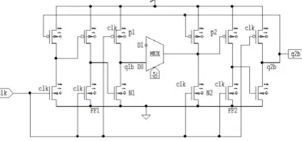
The Fig.7 Shows the Schematic of proposed E-TSPC-based divide-by-2/3 counter using multiplexer circuit implementation. According to the simulation results given in Fig 7, E-TSPC design shows the best power and speed performance in various counter designs including the one using conventional transmission gate FFs. Speed advantage, E-TSPC FFs are particularly useful for low voltage operations because of the minimum height in transistor stacking .Other than the two E-TSPC FFs, only one MUX is needed. The MUX controlled by the divide control signal serves as the switch .The proposed design scheme is far more sophisticated than the measure of simply adding one MUX compare to previous method. The circuit simplification, again, suggests the improvements in both speed and power performances.
Fig 7: Schematic of proposed E-TSPC-based divide-by-2/3 counter using multiplexer
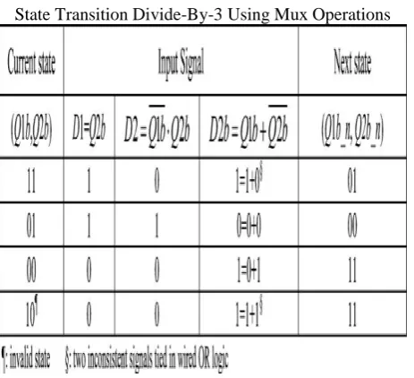
The working principle of the proposed 2/3 counter using MUX design is elaborated as follows. When the input signal D0,D1 is mainly depands on the signal DC value. When DC is “0”, the output of FF1, is tied with the output node of the 1st stage inverter of FF2 through the MUX. In an E-TSPC FF design, the output of the first stage inverter can be regarded complementary to the input,D.,i.e.,D’. When the signal DC=1 means MUX output is “0”.Otherthen DC=0,the output of FF1 is Q1b. Q2b is the inverted output of Q1b. By applying Demorgan’s law D2B=QIb+Q2b’ and D2B’=D2=Q1B’.Q2b to the Boolean equation gives rise to , which is exactly the desired logic. Table I shows the state transition table and the excitation logic of (Q1b,Q2b) when working in the divide-by-3 mode. The circuit is implemented by connecting the output node of FF1 (Q1b) and the output node of the 1st stage inverter in FF2 through a MUX circuit. Any signal inconsistence between these two nodes must be resolved by way of MUX. In other words, signal “1” must override signal “0”. In Table I, there exist two cases of such signal inconsistence. Case 1 occurs when both Q1b and Q2b are equal to “1”.When,clk=’0’ node D2b is both driven low by a pull down nMOS transistor N2 and pulled high by Q1b through MUX. Note Q1b that is actually a weak “1” retaining its level via parasitic capacitance.
V.
SIMULATION RESULTS4.1 E-TSPC-Based Divide-By- 2/3 Counter Design(a)
A state-of-the-art divide-by-2/3 counter design contains two E-TSPC-based FFs and two logic gates i.e., an OR gate and an AND gate. When the divide control signal is “0”, the OR gate (merged into output of FF1 design) is disabled. The state of cycles through 11, 01, and 00. This corresponds to a divide-by-3 function. Note that state10 is a forbidden state. If, somehow,the circuit enters this state, the next state will go back to a valid state,11, automatically. When is “1”, the output of FF1 will be disabled and FF2 alone performs the divide-by-2 operation.
IF DC=1
Fig 8.1(a): Output Waveform
IF DC=0
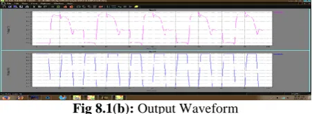
The Fig 8.1(b) shows the output waveform of E-TSPC based 2/3 counter design(a) existing circuit with the input of DC=0,which performs divide-by-3 operation,clock signal =10101010 and the output Q2b shows 3 toggles is equal to 1 rising and 1 falling in the waveform , first stage of the signal shows output with some distortion and second stage shows the input clock signal respectively. The below fig 8.1(b) shows the screenshot of DC=0. Since the input to FF1 is not disabled, FF1 toggles as usual and causes redundant power consumption in the divide-by-2 mode operation.
Fig 8.1(b): Output Waveform
4.2 E-TSPC-Based Divide-By- 2/3 Counter Design (b)
IF DC=1
The Fig.8.2(a) shows the output waveform of E-TSPC based 2/3 counter design(b), existing circuit with the input of DC=1,which performs divide-by-2 operation,clock signal =10101010 and the output Q2b shows 2 toggles is equal to 1 rising and 1 falling in the waveform.
Fig 8.2(a): Output Waveform
The first stage of the signal shows output with more distortion, third stage shows the input clock signal and second stage of this waveform shows inbuild dc value is always set as 5V respectively.
IF DC=0
The Figure 8.2(b) shows the output waveform of E-TSPC based 2/3 counter design(b),existing circuit with the input of DC=0,which performs divide-by-3 operation,clock signal =10101010 and the output Q2b shows 3 toggles is equal to 1 rising and 1 falling in the waveform.
Fig 8.2(b): Output Waveform
4.3 Double Inversion Technique
Fig 8.3: Double Inversion
4.4 E-TSPC-Based Divide-By- 2/3 Counter Design (a), double inversion
IF DC=1
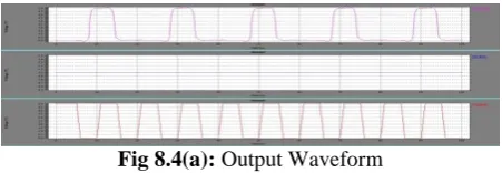
The Fig.8.4(a) shows the output waveform of E-TSPC based 2/3 counter design(a)with inverter, existing circuit with the input of DC=1,which performs divide-by-2 operation,clock signal =10101010 and the output Q2b shows 2 toggles is equal to 1 rising and 1 falling in the waveform.
Fig 8.4(a): Output Waveform
The first stage of the signal shows output with no distortion, third stage shows the input clock signal andsecond stage of this waveform shows inbuild dc value is always set as 5V respectively.
IF DC=0
The Fig.8.4(b) shows the output waveform of E-TSPC based 2/3 counter design(a)with inverter, existing circuit with the input of DC=0,which performs divide-by-3 operation,clock signal =10101010 and the output Q2b shows 3 toggles is equal to 1 rising and 1 falling in the waveform The first stage of the signal shows output with no distortion, third stage shows the input clock signal andsecond stage of this waveform shows inbuild dc value is always set as 5V respectively.
Fig 8.4(b): Output Waveform
4.5 E-TSPC-Based Divide-By- 2/3 Counter Design (b) With double inversion
IF DC=1
The Fig.8.5(a) shows the output waveform of existing circuit design (b) under the condition of DC=1 which performs divide-by-2 operation, due to critical path delay formed by the two Flip flops and control logic , is the dominant factor of the maximum operating frequency.
Fig 7.5(a): Output Waveform
IF DC=0
Fig 8.5(b): Output Waveform
4.6 Layout Of Existing Designs
The Fig.8.6(a) shows the layout design of existing circuit design (a)
Fig 8.6(a): Layout Design
The Fig.8.6(b) shows the layout design of existing circuit design (b)
Fig 8.6(b): Layout Design
4.7 Proposed E-TSPC-Based Divide-By-2/3 Counter Design With Pass Transistor Logic Circuit Technique
IF DC=1
The Fig.8.7(a) shows the output waveform of Proposed circuit design (a) under the condition of DC=1 which performs divide-by-2 operation, due to critical path delay formed by the two Flip flops and control logic.
Fig 8.7(a): Output Waveform
IF DC=0
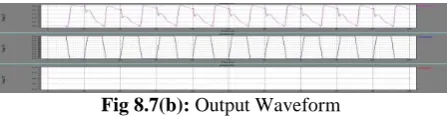
The Fig.8.7(b) shows the output waveform of E-TSPC based 2/3 counter design of proposed circuit with the input of DC=0,which performs divide-by-3 operation,clock signal =10101010 and the output Q2b shows 3 toggles is equal to 1 rising and 1 falling in the waveform first stage, of the signal shows output with no distortion, and second stage of this waveform shows inbuild dc value is always set as 5V respectively.
Fig 8.7(b): Output Waveform
4.7.1 Proposed Layout Design
Post-layout simulations in MicroWind are conducted to compare the performances between the proposed design and the two divide-by-2/3 counter designs shown in Fig.8.7, which are considered two of the best prior arts. And any performance discrepancy would come from the logic structure. However, designs in (a) and(b) are excluded as their stacked logic structures significantly degrade their speed performance when working in the territory of low . The target technology is TSMC 0.18 m 1P/6M CMOS process.
4.8 Proposed E-TSPC-Based Divide-By-2/3 Counter Design With Multiplexer
IF DC=1
The Fig.8.8(a) shows the output waveform of Proposed circuit design with multiplexer under the condition of DC=1 which performs divide-by-2 operation, due to critical path delay formed by the two Flip flops and control logic.
Fig 8.8(a): Output Waveform
IF DC=0
The Fig.8.8(b) shows the output waveform of Proposed circuit design with multiplexer under the condition of DC=0 which performs divide-by-3 operation, due to critical path delay formed by the two Flip flops and control logic.
Fig 8.8(b): Output Waveform
4.8.1 Layout Design Of Proposed Method With Multiplexer
Fig 8.9: Layout Design of proposed circuit The target technology is TSMC 0.18 m 1P/6M CMOS process.
TABLE I
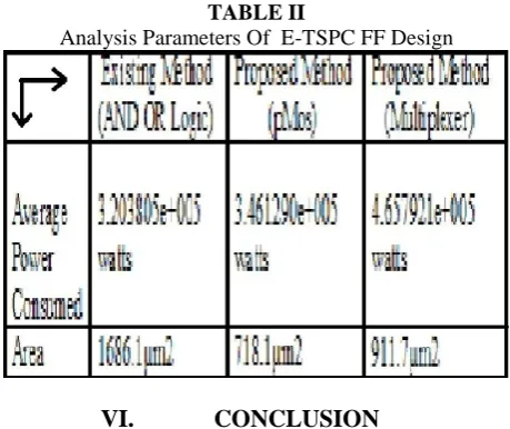
TABLE II
Analysis Parameters Of E-TSPC FF Design
VI.
CONCLUSION
Besides the fixed-modulus dividers, dual-modulus counters can also be synthesized in a similar way by using more than one TSPC DFFs and additional feedback logic gates. The proposed divide-by-2/3 counter design which is suitable for high speed applications is presented. The proposed divide-by-2/3 counter design which is suitable for high speed applications is presented. The proposed design successfully simplifies the control logic and one PMOS transistor alone serves the purposes of both mode select and counter excitation logic. The circuit simplicity leads to a shorter critical path and reduced power consumption.
REFERENCES
[1]. Yin-Tsung Hwang and Jin-Fa Lin , “Low voltage and Low Power Divide-By-2/3 Counter Design Using Pass Transistor Logic Circuit Technique,’’IEEE Trans. Circuit Syst.vol. 20,No. 9,Sep 2012. [2]. Deng .Z and Niknejad. A.M., “The speed-power trade-off in the design of CMOS true-
single-phase-clock dividers,” IEEE J. Solid-State Circuits,vol. 45, no. 11, pp. 2457–2465, Nov. 2010.
[3]. Krishna. M. V., Do. M. A., Yeo. K. S., Boon. C. C., and Lim. W. M.,“Design and analysis of ultra low power true single phase clock CMOS 2/3 prescaler,” IEEE Trans. Circuits Syst. I, Reg. Papers, vol. 57, no.1, pp. 72–82, Jan. 2010.
[4]. Lo. Y.-L., Chao. T.-S., and Cheng. K.-H., “High speed and ultra low voltage divide-by-4/5 counter for frequency synthesizer,” IEICE Trans.Electron., vol. E92-C, no. 6, pp. 890–893, Jun. 2009.
[5]. Yu. X.-P.,Do. M. A., Lim. W.M., Yeo. K. S., and Ma. J. G., “Design and optimization of the extended true single-phase clock-based prescaler,”IEEE Trans. Microw. Theory Techn., vol. 54, no. 11, pp. 3828–3835,Nov. 2006.
[6]. Rana. R. S., “Dual-modulus 127/128 FOM enhanced prescaler design in 0.35 um CMOS technology,”
IEEE J. Solid-State Circuits, vol. 40,no. 8, pp. 1662–1670, Aug. 2005.
[7]. Pellerano. S., Levantino. S., Samori.C, and Lacaita.A . L, “A 13.5-mW 5-GHz frequency synthesizer with dynamic-logic frequency divider,” IEEE J. Solid-State Circuits, vol. 39, no. 2, pp. 378–383, Feb. 2004.
[8]. Wong.J.M.C, Wong.C, Cheung.V.S.L, and Luong.H.C, “A 1-V 2.5-mW 5.2-GHz frequency divider in a 0.35-um CMOS process,” IEEE J. Solid-State Circuits, vol. 38, no. 10, pp. 1643–1648, Oct. 2003. [9]. Soares.J.N, Jr and Van Noije.W.A.M, “Extended TSPC structures with double input/output data
throughput for gigahertz CMOS circuit design,” IEEE Trans. Very Large Scale Integr. (VLSI) Syst., vol. 10, no. 3, pp. 301–308, Jan. 2002.
[10]. Soares.J.N, Jr and Van Noije.W.A.M, “A 1.6-GHz dual modulus prescaler using the extended true-single-phase-clock CMOS circuit technique (E-TSPC),” IEEE J. Solid-State Circuits, vol. 34, no. 1, pp. 97–102, Jan. 1999.
[11]. Chang.B, Park.J, and Kim.K, “A 1.2 GHz CMOS dual-modulus prescaler using new dynamic D-type flip-flops,” IEEE J. Solid-State Circuits, vol. 31, no. 5, pp. 749–752, May 1996.
[12]. Huang.Q and Rogenmoser.R, “Speed optimization of edge-triggered CMOS circuits for gigahertz single-phase clocks,” IEEE J. Solid-State Circuits, vol. 31, no. 3, pp. 456–465, Mar. 1996.