e
-ISSN: 2250-3021,
p
-ISSN: 2278-8719
Vol. 3, Issue 11 (November. 2013), ||V1|| PP 21-28
Structural, optical and electrical
properties of TiO
2thin films
synthesized by sol–gel technique
F. Hanini, A. Bouabellou, Y. Bouachiba, F. Kermiche, A. Taabouche,
M. Hemissi, and D. Lakhdari
1
Laboratoire Couches Minces – Interfaces, Université Constantine 1, 25000, Algérie.
2
Laboratoire Dosage, Analyse et Caractérisation en Haute Résolution, Université Ferhat Abbas-Sétif, Algerie.
3
Unité de Développement de la Technologie du Silicium 02.BP.N°:140 Alger-7 Merveilles, Algérie.
Abstract: - The influence of annealing temperature on the structure, optical andelectrical property of TiO2 thin
films with (101) preferential orientation were deposited on glass substrates by sol–gel technique has been studied. As-deposited films were amorphous, and the XRD studies showed that the formation of anatase phase was initiated at annealing temperature close to 400 °C. The grain size of the film annealed at 550 °C was about 22 nm. The transmission spectra, recorded in the UV visible range reveal a relatively high transmission coefficient (~70%) in the obtained films. The transmittance data analysis indicates that the optical band gap (Eg)
is closely related to the annealing temperature, an indirect band gap ranging from 3.43 eV to 3.04 eV was deduced.The electrical resistivity measurement that were carried out in function of the annealing temperature showed a sharp decrease in resistivity was found to be 0.0802 .cm.
Keywords: TiO2 Thin films, Annealing, DRX, Anatase,Optical property, Resistivity
I. INTRODUCTION
Among available techniques, sol-gel. Technique has emerged as one of the most promising technique as this method produces samples with a good homogeneity at low cost. In addition, sol gel processing is particularly efficient in producing thin, transparent, multi-component oxide layers of many compositions on many substrates, including glass. This is especially attractive for enterprises engaged in flexible on-demand fabrication as well as for small- and mid-sized companies that refrain from the high investment costs required for vacuum based technologies [1]. TiO2 is a wide band gap semiconductor material which has been under
extensive investigations due to its applications in a variety of fields such as dye-sensitized solar cell [2], gas sensors [3], photocatalysts [4-5], waveguiding [6], antireflective coatings [7], dielectric [8], etc. Titanium dioxide (TiO2) belongs to the family of transition metal oxides [9]. In nature, TiO2 is known to occur in the
structures of rutile, anatase, and brookite (brookite is a minority product of most synthesis) [10]. A fourth polymorph, having the α-PhO2 structure (orthorhombic), has recently been synthesized under high-pressure [11].
In nature, TiO2 is known to occur in the structures of rutile, anatase, and brookite (brookite is a minority product
of most synthesis) [10]. A fourth polymorph, having the α-PhO2 structure (orthorhombic), has recently been
synthesized under high-pressure [11]. The structures of rutile, anatase and brookite can be discussed in terms of (
TiO
26) octahedrals are interconnected differently for each phase, leading to different structures and symmetries [9]. Many important applications of TiO2 depend on its structural, electrical and optical propertiesbecause of their excellent properties, e.g. chemical and physical stability, high refractive index, good transmission in VIS and NIR regions, high dielectric constants, high electrical resistance and interesting catalytic properties. For as-deposited films that are mostly amorphous, post-deposition annealing is the key factor to modify microstructure of the films. Films with dense structure are good in solar cell applications where as porous films are better for gas sensors. Rutile phase has good stability and high refractive index which makes it suitable for protective coatings on lenses [12]. The anatase phase which has better response with ultraviolet photons is used for photocatalysis [13] where as amorphous TiO2 films are utilized in biomedical
fields due to its blood compatibility [14]. In this work, we study the effect of annealing level on the structural, optical and electrical properties of TiO2 films synthesized by sol-gel method.
II. EXPERIMENTAL DETAILS
cm/min and dried at 100°C during 15 min. Finally, the obtained samples have been annealed under oxygen O2
flux at temperatures from 400 to 550 °C for 20 min.
The structural characterization of the films was carried out by ray diffraction technique using an X-ray diffractometer (PHILIPS XPERT-PRO) with CuKα radiation. The optical transmittance was measured on a Shimadzu 3101 PC UV–visible spectrophotometer. The electrical resistivity of the films was measured in a coplanar structure obtained with evaporation of two golden stripes on film surface.
From the XRD pattern the grain size of TiO2 thin films were estimated for all the observed planes by using the
Scherer’s formula [15].
cos
) (k
D
nm
(1)where k varies from 0.89 to 1.39. But in most of the cases it is closer to 1. Hence for grain size calculation it is taken as one, λ is wavelength of X-ray, β is the full-width at half of the peak maximum in radians and θ is Bragg’s angle
The microstrain () developed in the TiO2 thin films was calculated from the equation as [16]
cos
D
sin
1
(2)where β is full-width at half-maximum of the (101) peak and D is the average grain size.
The refractive index (nf) of the films was calculated using the envelope method, described in reference [17].
2 2
s
f
N
N
n
n
(3) Where2
1
.
2
2
s m M m M sn
T
T
T
T
n
N
(4)TM and Tm are, respectively, the maxima and minima of the envelope in the transmittance spectra, and ns is the
refractive index of the glass which can be calculated from the transmittance Ts of the glass using Eq. (6) [18].
The transmittance of the glass was 90% in the wavelength range 300–900 nm.
2 1 2
1
1
1
s s sT
T
n
(6)The thickness of the film was calculated using the following relation [17]:
1 2 2 1
2 12
n
n
d
(7)where n1 and n2 are the refractive indices at the two adjacent maxima (or minima) at 1 and 2. The titanium
oxide film thickness was found to be 0.17 µm.
The measured films thicknesses of our films were between 177 nm and 230 nm. The absorption coefficient of TiO2 films was determined from transmittance measurements. The films’ absorption coefficient was calculated
using the following expression [17]:
d
T
/
1
ln
(8)where T is the transmittance of the film at each wave length and d is the thickness of the film The band gap Eg was calculated using the Tauc equation [18,19];
h
E
h
k
g n
(9)where k is a constant, hν is the photon energy (eV), and the value of n can be 1/2 or 2 depending on whether it is direct or indirect transitions.
The porosity of the TiO2 films, defined as the ratio of the film density f to the bulk density b, is calculated
using the following relation [20]:
1
2
2
1
1
-1
Porosity
22 2 2 b b f f fb f
n
n
n
n
(10)where nbis the refractive index of pore free anatase TiO2 which is having a refractive index of 2.52 at 550 nm
The absorption coefficient of films shows a tail for sub-band gap photon energy his tail is so-called Urbach tail. The latter, which is closely related to the disorder in the film network, is expressed as [22].
u
E
h
0exp
(11)where 0 is a constant and Euis the Urbach energy.
III. RESULTS AND DISCUSSION
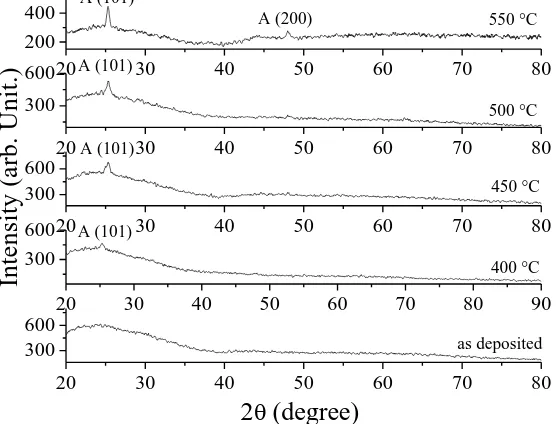
The XRD patterns of the films annealed at different temperatures are shown in Fig. 1. As seen, the obtained diffraction patterns show predominant peak at 25.30° which can be assigned to the (101) plane of anatase TiO2is found to begin at approximately 400°C. At 550°C a very sharp exothermic peak is observed due
to the formation of anatase phase [23]. No peaks related to either the rutile or brookite phases were observed in the XDR patterns. The films as deposited were amorphous in nature. With the increase of annealing
temperature there is an increase in intensity and sharpening of this peak, which is caused by improving crystallinity of the films.
The obtained grain size values are reported in Table 1. The grain size of the films annealed at 400 °C was about 13.51 nm and increased to 21.72 nm after annealing at 550 °C. This trend is climbed by many authors [21,23].
20 30 40 50 60 70 80
300 600
20 30 40 50 60 70 80 90
300
60020 30 40 50 60 70 80
300 600
20 30 40 50 60 70 80
300
60020 30 40 50 60 70 80
200
400 550 °C
450 °C 500 °C
400 °C A (200)
as deposited A (101)
A (101)
A (101) A (101)
In
te
n
si
ty
(
a
rb
.
U
n
it
.)
2
(degree)
Fig. 1. X-ray diffraction patterns of TiO2 thin films on glass substrates before and after annealed at different
temperatures
Table 1. Structural parameters of TiO2 thin films annealed at different temperatures
Parameter Standard pattern Measured pattern Annealing temp. (°C)
TiO2–anatase (21–1272) as-deposited 400 450 500 550
2 (°) 25.45
Amorphous nature
25.30 25.31 25.45 25.34
d (nm) 3.521 3.517 3.516 3.497 3.511
D (nm) -- 13.510 15.352 18.262 21.721
ε× 10-3 -- 6.346 5.850 4.678 4.388
Data have been estimated with respect to the most intense anatase [24] peak (1 0 1) at 2 =25.453°, d–inter planar distance, D–grain size, ε–microstrain.
The calculated values are given in Table 1. It is clear that when the annealing temperature is increased the strain decreased considerably. This type of microstrain changes may be due to the predominant recrystallization process in the polycrystalline thin films.
Fig. 2illustrates the three-dimensional (3D) atomic force microscopic (AFM) images of TiO2 thin films
Figure 2 shows the UV-vis transmittance spectra of TiO2 films heat treated at different temperatures.
As can be seen, an increase in the annealing temperature improves the films optical transmission. Obviously, the films are fully transparent in the visible region and a sharp fall in the UV region 300-400 nm.
300
400
500
600
700
800
0
20
40
60
80
100
0 100 200 300 400 500 600 3,36
3,40 3,44 3,48 3,52 3,56 3,60
T (°C)
A
b
s
o
r
p
ti
o
n
e
d
g
e
(
e
V
)
Wavelength (nm)
T
ra
n
s
m
it
ta
n
c
e
(
%
)
as deposited
400 °C
450 °C
500 °C
550 °C
Fig. 2. UV–vis transmittance spectra of TiO2 thin films on glass substrates before and after annealed at different
temperatures. In inset, the absorption edge derived from transmittance data vs annealing temperature.
With increasing the annealing temperature, the absorption edge shifts towards lower energy side, indicating the decrease in the band gap. Indeed, a quantitative analysis of the absorption edge shifts (showed in inset of Fig. 2) leads to a very good agreement with those of the band gap energies depicted in Fig. 5.
The fringes visible in Fig. 2 result from the multiple interference of the light reflected from the two optical interfaces: (1) air-thin film and (2) thin film-substrate. In order to determine the thickness and refractive index parameters of the thin film (see Table 2).
Table 2. Thickness, refractive index and band gap of TiO2 films determined using optical transmission spectra
Annealing temp. (°C) Thickness (nm) Refractive index n at 550 nm Band gap Eg (eV)
As-deposited 232.49 1.63 3.42
400 205.56 1.67 3.37
450 203.04 1.79 3.36
500 194.13 1.89 3.14
550 177.82 2.05 3.04
0 100 200 300 400 500 600 1,5
1,6 1,7 1,8 1,9 2,0 2,1 2,2 2,3
T (°C)
Refractive index Porosity
15 20 25 30 35 40 45 50
As-deposited
R
e
fr
a
c
ti
v
e
i
n
d
e
x
P
o
ro
si
ty
(
%
)
Fig. 3. Variation of the refractive index at 550 nm and porosity of TiO2 films as a function of annealing
temperature. The data corresponding to the as-deposited samples are taken at 25 °C.
Figure 3 depicts the variations of the porosity and the refractive index of the TiO2 films as a function of
annealing temperature. There, we found that the porosity of the films gradually decreases with increasing annealing temperature: a behaviour which provides a direct evidence for the correlation between the porosity and the refractive index of the TiO2 films. This observation supports our above explanation that one of the
reasons for the decrease in band gap with annealing temperature can be the densification of the films.
The optical gap and the Urbach tail energy are estimated from the absorption coefficient variation, as described in Fig. 4a and b shows a typical variation of (hv)1/2 and ln drawn as a function of photon energy respectively.
Fig. 4a is used to extrapolate the optical band gap, while Fig. 4b is used to deduce the Urbach band tail width.
Fig. 4. Typical variation of (h)1/2 and ln drawn as a function of photon energy used respectively for: (a)
optical band gap and (b) Urbach tail width determination
It is worth noticing that the as deposited films (amorphous) are characterized by a high optical energy gap value of 3.43 eV. The thermal annealing at 400-550 °C the crystalline structure of TiO2 films in the anatase
phase is almost improved and Eg decreases drastically to the value of 3.04 eV. On the other hand, it is worth
mentioning that previous investigations have also reported a decrease in the optical band gap of the TiO2 films
with annealing temperature might be the result of the change in film density and increase in grain size [27]. Fig. 5 shows the change in optical band gap with the grain size.
1,0 1,5 2,0 2,5 3,0 3,5 4,0
11 12 13 14
ln
cm
-1
h
eV
Eu
=508.43
meV
(b)
1,0 1,5 2,0 2,5 3,0 3,5 4,0
0 500 1000 1500 2000 2500
h
eV
(
h
)
1
/2
(
cm
-1
eV
)
1
/2
Eg
= 3.04
eV
12 14 16 18 20 22 3,0
3,1 3,2 3,3 3,4
3,5 400 °C
550 °C
B
an
d
G
ap
(
eV
)
Grain size (nm)
Fig. 5. The variation of optical band gap with grain size of the films.
Fig. 6 shows the variations of the optical gap together with the Urbach tail energy as a function of annealing temperature. The variation of the film disorder as a function of annealing temperature is represented in Fig. 6. As seen the films become more organized with increasing the annealing temperature due to the reduction of the disorder. On the other hand the increase in the optical band gap corroborates well with the disorder reduction in films' network. This indicates clearly that the optical gap in the obtained films is governed by the disorder. As depicted in the insert in Fig. 6, showing the bands bending in a semiconductor, an increase in the band tail width causes the reduction in the optical gap.
0 100 200 300 400 500 600
3,05 3,10 3,15 3,20 3,25 3,30 3,35 3,40 3,45
U
rb
a
c
h
e
n
e
rg
y
(
m
e
V
)
B
a
n
d
G
a
p
(
e
V
)
T (°C)
Band Gap)
Urbach energy
375 400 425 450 475 500
Eg Eu
EV
EC
Fig. 6. Variation of optical band gap and Urbach energy with of TiO2 films as a function of annealing
temperature.
We conclude from the XRD analysis that films are composed with microcrystallites embedded in amorphous phase. This amorphous phase is the origin of the disorder measured in the film network. Bearing in mind that the disorder is defined as the deviation of the bond length and angle from their standard values in the crystalline material, therefore with increasing the annealing temperature the amorphous phase becomes more organized due to the reduction of the disorder.
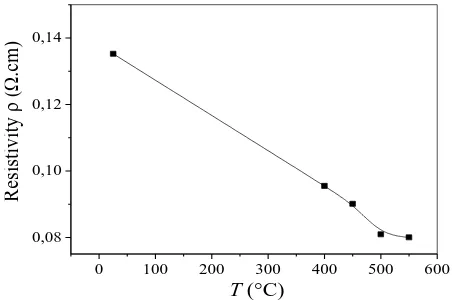
Fig. 7shows the variation of the resistivity, ρ, of TiO2 thin films as a function of annealing temperature.
The obtained results indicate that the resistivity of the samples decreases with the increase in annealing temperature and reached its minimum value of 0.0802 .cm with afilms annealed at 550 °C.This resistivity behaviour is due, on the one hand, to the increase in the regular sites of the Ti atoms in the films network. Since TiO2 is an n-type semiconductor, the concentration of Ti4+ in TiO2 films forms a donor level between the band
gap of TiO2 which results in the reduction of recombination of photogenerated electrons and holes [28,29].
0 100 200 300 400 500 600 0,08
0,10 0,12 0,14
R
es
is
ti
v
it
y
.cm
)
T (°C)
Fig. 7. The dependence of film resistivity on annealing temperature.
On the other hand, the increase in the conductivity (decrease of resistivity) with annealing temperatures can be also explained as follows: the grain size increases with annealing temperature which leads to a decrease in grain boundaries and hence resistivity [30].
IV. CONCLUSION
Titanium oxide thin films were deposited on glass substrates by sol–gel technique and then submitted to an annealing treatment in the range of temperatures 400-550°C. Annealing effect on the structural, optical and electrical properties of TiO2 films was investigated. XRD studies reveal that the material in the thin form is
polycrystalline (anatase) with a preserve their (101) preferential orientation. The grain size was calculated to be 22 nm. The indirect band gap raised from 3.04 to 3.43 eV. So, the films had a transmittance of more than 70% in the visible region. Hence, the decrease in resistivity allows the correlation between the results obtained by X-ray diffraction and optical properties of TiO2 thin films synthesized by sol-gel method.
REFERENCES
[1] C.J. Brinker, G.W. Scherer, Sol–Gel Science-The Physics and Chemistry of Sol–Gel Processing, Academic Press, Boston, USA, 1990.
[2] Antonio Otávio T. Patrocínio, Eucler B. Paniago, Roberto M. Paniago, Neyde Y. Murakami Iha, Appl. Surf. Sci 254 (2008) 1874–1879.
[3] Ibrahim A. Al-Homoudi, J.S. Thakur, R. Naik, G.W. Auner, G. Newaz, , Appl. Surf. Sci 253 (2007) 8607–8614.
[4] M.R. Hoffmann, S.T. Martin,W. Choi, D.W. Bahnemann, Chem. Rev. 95 (1995) 69–96. [5] X.Z. Li, H. Liu, L.F. Cheng, H.J. Tong, Environ. Sci. Technol. 37 (2003) 3989–3994.
[6] R. Mechiakh, F. Meriche, R. Kremer, R. Bensaha, B. Boudine, A. Boudrioua , Optical Materials 30 (2007) 645–651.
[7] Sang-Hun Jeong, Jae-Keun Kim, Bong-Soo Kim, Seok-Ho Shim, Byung-Teak Lee, Vacuum 76 (2004) 507–515.
[8] Wenli Yang, Colin A. Wolden, Thin Solid Films 515 (2006) 1708–1713.
[9] O. Carp, C.L. Huisman, A. Reller, Progress in Solid State Chemistry 32 (2004) 33–177 [10] Y.F. Chen, C.Y. Lee, M.Y. Yeng, H.T. Chiu, Mater. Chem. Phys. 81 (2003) 39–44.
[11] D.W. Meng, X.L. Wu, F. Sun, L.W. Huang, F. Liu, Y.J. Han , J.P. Zheng, X. Meng, R. Mason, Micron 39 (2008) 280–286.
[12] H.Takikawa, T.Matsui, T. Sakakibara, A. Bendavid, P.J. Martin,. Properties of titanium oxide film prepared by reactive cathodic vacuum arc deposition. Thin Solid Films 348 (1999)145–151.
[13] J. Yu, X. Zhao, Q. Zhao, Photocatalytic activity of nanometer TiO2 thin films prepared by the sol-gel
method. Materials Chemistry and Physics b 69 (2001) 25–29.
[14] J. Liu, D. Yang, F. Shi, Y. Cai, Sol-gel deposited TiO2 film on NiTi surgical alloy for biocompatibility
improvement. Thin Solid Films 429 (2003) 225–230.
[15] Bin Zhou, Meghan Schulz, H.Y. Lin, S. Ismat Shah, Jiuhui Qu, C.P. Huang, Applied Catalysis B: Environmental 92 (2009) 41–49.
[16] B. D. Cullity, Elements of X ray Diffraction, Addition, Wesley Pub, Note Dame, 1978. [17] M. Hemissi, H. Amardjia-Adnani, J.C. Plenet, Current Applied Physics 9 (2009) 717–721.
[19] M. M. Abdel-Aziz, I.S. Yahia, L.A. Wahab, M. Fadel and M.A. Afifi, Appl. Surf. Sci. 252 (2006) 8163-8170.
[20] M. Born, E. Wolf, Principles of Optics, Pergamon, New York, 1975, p. 85.
[21] Ya-Qi Hou, Da-Ming Zhuang, Gong Zhang, Ming Zhao, Min-Sheng Wu, Applied Surface Science 218 (2003) 98–106.
[22] M. Pal, Y. Tsujigami, A. Yoshikado, H. Sakata, Phys. Status Solidi, A. Appl. Res. 182 (2000) 727. [23] Jiaguo YuU, Xiujian Zhao, Qingnan Zhao, Thin Solid Films 379(2000) 7-14.
[24] Natl. bur. Stand. (U.S.) 25, 7, 82 (1969).
[25] M. H. Suhail, G. Mohan Rao, S. Mohan, J. Appt. Phys. 71 (1992) 1421-1427. [26] M. Born, E. Wolf, Principle of optics., Pergamon, New York (1975)
[27] C.V.R. Vasanth Kumar and A. Mansingh. J. Appl. Phys. 65 (1989)1270. [28] M. A. MALATI and W. K. WONG, Surface Technology, 22 (1984) 305-322.
[29] Xiujian Zhao, Qingnan Zhao, Jiaguo Yu, Baoshun Liu, Journal of Non-Crystalline Solids 354 (2008) 1424–1430.