University of Pennsylvania
ScholarlyCommons
Publicly Accessible Penn Dissertations
Spring 5-16-2011
Microbead-Based Biosensing in Microfluidic
Devices
Jason A. Thompson
University of Pennsylvania, [email protected]
Follow this and additional works at:http://repository.upenn.edu/edissertations
Part of theAnalytical Chemistry Commons,Biology Commons, and theMechanical Engineering Commons
Recommended Citation
Microbead-Based Biosensing in Microfluidic Devices
Abstract
Microbeads are frequently used as a solid support to capture target analytes of interest, such as proteins and nucleic acids, from a biological sample. The integration of microbeads into microfluidic systems for biological testing is an area of growing interest. Such "lab-on-chip" systems are designed to integrate several functions of a conventional laboratory onto a single chip. As a platform to capture targets, beads offer several advantages over planar surfaces such as large surface areas to support biological interactions (increasing sensitivity), the availability of libraries of beads of various types from many vendors, and array-based formats capable of detecting multiple targets simultaneously (multiplexing). This dissertation describes the development and characterization of microbead-based biosensing devices. A customized hot embossing technique was used to stamp an array of microwells in a thin plastic substrate where appropriately functionalized agarose microbeads were selectively placed within a conduit. Functionalized quantum dot nanoparticles were pumped through the conduit and used as a fluorescent label to monitor binding to the bead. Three-dimensional finite element simulations were carried out to model the mass transfer and binding kinetics on the beads’ surfaces and within the porous beads. The theoretical predictions were critically compared and favorably agreed with
experimental observations. A novel method of bead pulsation was shown to improve binding kinetics in porous beads. In addition, the dissertation discusses other types of bead arrays and demonstrates alternative bead-based target capture and detection strategies. This work enhances our understanding of bead-based microfluidic systems and provides a design and optimization tool for developers of point-of-care, lab-on-chip devices for medical diagnosis, food and water quality inspection, and environmental monitoring.
Degree Type Dissertation
Degree Name
Doctor of Philosophy (PhD)
Graduate Group
Mechanical Engineering & Applied Mechanics
First Advisor Haim H. Bau
Keywords
Microbeads, Biosensors, Microfluidics, Numerical Simulation, Agarose Beads, Microbead Arrays
Subject Categories
MICROBEAD-BASED BIOSENSING IN
MICROFLUIDIC DEVICES
Jason A. Thompson
A DISSERTATION
in
Mechanical Engineering and Applied Mechanics
Presented to the Faculties of the University of Pennsylvania
in
Partial Fulfillment of the Requirements for the
Degree of Doctor of Philosophy
2011
Supervisor of Dissertation
______________________________
Haim H. Bau, Professor, Mechanical Engineering and Applied Mechanics
Graduate Group Chairperson
______________________________
Jennifer R. Lukes, Associate Professor, Mechanical Engineering and Applied Mechanics
Dissertation Committee
Haim H. Bau, Professor, Mechanical Engineering and Applied Mechanics Howard H. Hu , Professor, Mechanical Engineering and Applied Mechanics
MICROBEAD-BASED BIOSENSING IN MICROFLUIDIC DEVICES
COPYRIGHT
2011
ACKNOWLEDGEMENTS
Many people have supported me throughout my graduate school career and made
the timely completion of this dissertation possible. First and foremost I would like to
thank my advisor, Dr. Haim Bau, for his steadfast guidance, wisdom, and encouragement.
I am deeply grateful for his hardworking mentality, reliability, and sincere interest in my
academic well-being. I also greatly appreciate the insights and experience of my other
dissertation committee members, Drs. Howard Hu, Paulo Arratia, and Barry Ziober. My
interactions with the Department of Mechanical Engineering and Applied Mechanics
(MEAM) faculty and staff, particularly Maryeileen Banford Griffith, Susan Waddington
Pilder, and Peter Szczesniak, have been both enjoyable and constructive. Funding from a
National Science Foundation Integrative Graduate Research Traineeship (IGERT Grant #
DGE-0221664) fellowship and a U.S. Department of Education Graduate Assistance in
Areas of National Need (GAANN) fellowship in Lab-On-Chip Technology enabled the
continuous pursuit of my research interests.
I would also like to recognize my colleagues in the Bau Lab for their friendship,
collaboration, and fruitful scientific conversations. Their camaraderie both in and out of
the lab made it fun to be a full-time graduate student. Thanks especially to Joe Grogan,
Mian Qin, Tong Gao, and Drs. Mark Arsenault, Hui Zhao, and Michael Schrlau.
Additionally I had the pleasure of working with a number of post-doctoral researchers in
the lab as well as mentoring several undergraduate students who joined our group for the
Thanks also to several individuals who supported specific sections of the
dissertation. Gladys Gray Lawrence kindly assisted with confocal microscopy training.
Kristi Reitnauer, a Penn Engineering undergraduate, helped perform the ESE Reader
measurements in Chapter 6. Dr. David Walt at Tufts University provided the microbeads
and reagents for the immunoassays in Chapter 7. Dr. Timothy Blicharz, a graduate of
Walt's group, graciously assisted with the assay.
Finally I would like to give a heartfelt thanks to my family for a lifetime of loving
support and encouragement. I realize every day how lucky I am, and how I simply would
ABSTRACT
MICROBEAD-BASED BIOSENSING IN MICROFLUIDIC DEVICES
Jason A. Thompson
Haim H. Bau
Microbeads are frequently used as a solid support to capture target analytes of
interest, such as proteins and nucleic acids, from a biological sample. The integration of
microbeads into microfluidic systems for biological testing is an area of growing interest.
Such "lab-on-chip" systems are designed to integrate several functions of a conventional
laboratory onto a single chip. As a platform to capture targets, beads offer several
advantages over planar surfaces such as large surface areas to support biological
interactions (increasing sensitivity), the availability of libraries of beads of various types
from many vendors, and array-based formats capable of detecting multiple targets
simultaneously (multiplexing). This dissertation describes the development and
characterization of microbead-based biosensing devices. A customized hot embossing
technique was used to stamp an array of microwells in a thin plastic substrate where
appropriately functionalized agarose microbeads were selectively placed within a
conduit. Functionalized quantum dot nanoparticles were pumped through the conduit and
used as a fluorescent label to monitor binding to the bead. Three-dimensional finite
element simulations were carried out to model the mass transfer and binding kinetics on
the beads’ surfaces and within the porous beads. The theoretical predictions were
method of bead pulsation was shown to improve binding kinetics in porous beads. In
addition, the dissertation discusses other types of bead arrays and demonstrates
alternative bead-based target capture and detection strategies. This work enhances our
understanding of bead-based microfluidic systems and provides a design and
optimization tool for developers of point-of-care, lab-on-chip devices for medical
TABLE OF CONTENTS
DEDICATION iii
ACKNOWLEDGEMENTS iv
ABSTRACT vi
TABLE OF CONTENTS viii
LIST OF FIGURES xi
CHAPTER 1: INTRODUCTION 1
1.1 Lab-On-Chip Technology and Microfluidics 1
1.2 Microbeads in Biosensing 3
1.3 Motivation for Research and Organization of Dissertation 8
CHAPTER 2: FABRICATION OF MICROWELL ARRAYS IN PLASTIC
BY HOT EMBOSSING AND ASSEMBLY OF MICROFLUIDIC CHIP 11
2.1 Introduction 11
2.2 Fabrication of Silicon Stamping Masters from Photolithography 12 2.2.1 Formation of Large Diameter, Tall Pins 12 2.2.2 Formation of Small Diameter, Short Pins 12
2.3 Fabrication of Aluminum Stamping Masters from CNC Machining 13
2.4 Hot Embossing of Microwell Arrays in Plastic 14 2.4.1 Embossing of Large Diameter, Tall Pins with Silicon Master 14 2.4.2 Embossing of Small Diameter, Short Pins with Silicon Master 15 2.4.3 Embossing of Large Diameter, Tall Pins with Aluminum Master 18
2.5 Assembly of Microfluidic Chip 18
2.6 Autofluorescence and Photobleaching in Bead-Based Microfluidic Chips 20
CHAPTER 3: NON-POROUS MICROBEAD AFFINITY ASSAY:
EXPERIMENTS AND FINITE ELEMENT SIMULATIONS 27
3.1 Introduction 27
3.2 Experiments 28
3.3 Mathematical Model and Numerical Method 31
3.4 Results and Discussion 37
3.5 Conclusions 49
CHAPTER 4: POROUS MICROBEAD AFFINITY ASSAY:
EXPERIMENTS AND FINITE ELEMENT SIMULATIONS 52
4.1 Introduction 52
4.2 Materials and Methods 55
4.2.1 Confocal Microscopy Experiments 55
4.2.2 Mathematical Model and Numerical Method 56
4.3 Results and Discussion 59
4.3.1 Propagation of Bound Complex Front 59 4.3.2 Determination of Bead's Properties 63 4.3.3 Finite Element and Combined Results 66
4.4 Bead Heterogeneity Due to Compression 71
4.5 Conclusions 77
CHAPTER 5: PULSATION OF POROUS BEADS 79
5.1 Introduction 79
5.2 Experiments 80
5.3 Results and Discussion 84
CHAPTER 6: FURTHER CHARACTERIZATION OF BEADS ON A CHIP 90
6.1 Introduction 90
6.2 Shelf Life of Bead Chips 90
6.3 Bead Measurements with ESE Handheld Fluorescent Reader 93 6.3.1 Binding Curves for Varying Analyte Concentration 95 6.3.2 Bead Fluorescence for Varying Reader Positions Relative to Chip 97
6.4 Conclusions 98
CHAPTER 7: RANDOMLY STRUCTURED BEAD ARRAYS FOR
ALTERNATIVE CHIP-BASED IMMUNOASSAYS 100
7.1 Introduction 100
7.2 Pouch-Based Immunoassay with Integrated Etched Silicon Bead Array 101
7.2.1 Experiments 103
7.2.2 Results and Discussion 105
7.3 Chip-Based Immunoassay with Integrated Embossed Plastic Bead Array 107
7.3.1 Experiments 107
7.3.2 Results and Discussion 109
7.4 Conclusions 114
CHAPTER 8: CONCLUSIONS 115
8.1 Summary of Research 115
8.2 Outlook 117
LIST OF FIGURES
Figure 1.1: A schematic depiction of the integration and miniaturization of
laboratory functions onto a chip (Chow 2002)... 2
Figure 1.2: Research groups and companies specializing in microbead-based
biosensing technology. (a) Dr. John McDevitt's group; LabNow, Inc. (b) Dr. David Walt's group; Illumina, Inc. (c) BioArray
Solutions, An Immucor Company. (d) Luminex Corporation... 7
Figure 2.1: Custom-fabricated hot embossing setup to stamp a microbead array
in a plastic substrate... 14
Figure 2.2: (a) Electron micrograph of silicon stamping master with large pins.
(b) Corresponding wells hot embossed in COC... 16
Figure 2.3: (a) Electron micrograph of silicon stamping master with small
pins. (b) Corresponding wells hot embossed in COC... 16
Figure 2.4: (a) Electron micrograph of CNC-machined aluminum stamping
master. (b) Corresponding wells hot embossed in COC... 18
Figure 2.5: (a) A schematic depiction of the experimental chip containing the
controllably assembled microbead array. (b) The same chip
containing the randomly assembled microbead array... 19
Figure 2.6: Experimental binding curve illustrating autofluorescence using
streptavidin-coated polystyrene beads and 1 nM biotin-QDot605
solution... 22
Figure 2.7: (a) Autofluorescence decay of streptavidin-coated polystyrene
beads under continuous illumination from an epifluorescence microscope. (b) Plot in (a) normalized by the maximum fluorescent
intensity of each bead... 22
Figure 2.8: Increased autofluorescence of high capacity streptavidin-coated
agarose beads due to continuous illumination from an
epifluorescence microscope... 24
Figure 3.1: Electron micrograph (650x magnification) of an embossed 2×2
microwell array loaded with dry agarose beads... 30
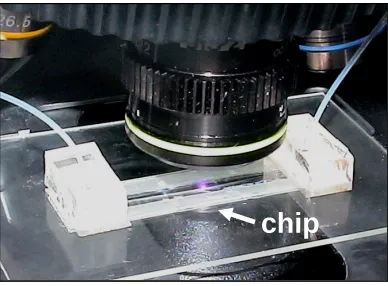
Figure 3.2: A photograph of the experimental chip mounted on the stage of an
Figure 3.3: A schematic depiction of the binding of biotin-QDot targets to
bead-immobilized streptavidin receptors. The receptors are coupled to the agarose bead's fiber matrix (SEM image of 2%
agarose fibers reproduced from Wong 2007)... 32
Figure 3.4: The bottom surface of an agarose bead partially covered with
bound QDots (20x objective)... 38
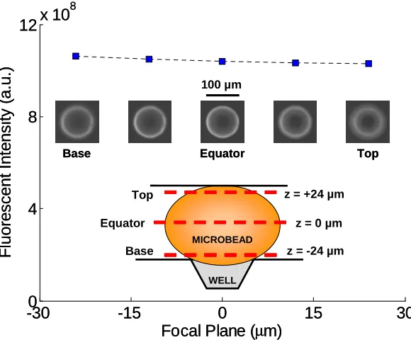
Figure 3.5: Measured fluorescent intensity of a conduit-immobilized bead
decorated with bound QDots as a function of focal plane position... 38
Figure 3.6: The computed flow field around an immobilized, compressed bead
with a non-slip boundary condition at its surface illustrated with
horizontal (a) and vertical (b) cross-sections... 42
Figure 3.7: The normalized bound complex on the bead's surface in the
absence of surface exclusion effects as a function of time for
various diffusion coefficients (a) and flow rates (b)... 42
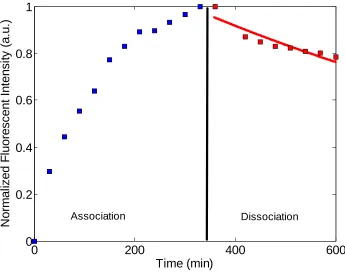
Figure 3.8: Experimental association (C~o= 20 nM) and dissociation curves.
The solid (red) curve is a single exponential fit to the experimental
dissociation data... 44
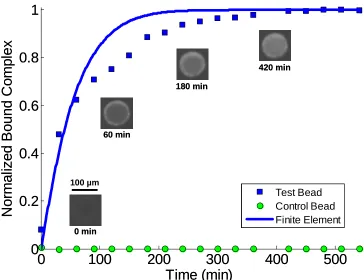
Figure 3.9: Normalized total bound complex as a function of time. The
symbols and line correspond, respectively, to experimental data
and theoretical predictions... 46
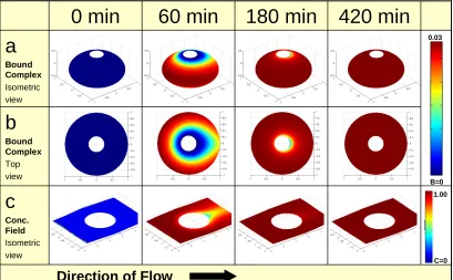
Figure 3.10: Finite element simulation results depicting the concentration of
QDots on and around the bead as functions of time for the same conditions as in Figure 3.9. (a) Isometric view of the bound complex. (b) Top view of the bound complex. (c) Isometric view
of the concentration field around the bead's midplane... 47
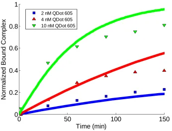
Figure 3.11: Experimental (symbols) and finite element results (lines) for the
normalized total bound complex as a function of time when C~o= 2,
4, and 10 nM... 48
Figure 4.1: Confocal fluorescent image showing the position of three agarose
beads in the array. The inset plot illustrates the definition of bound
Figure 4.2: (a) Propagation of QDot bound complex front toward the center of
each bead. (b) Penetration depth for each bead in (a) plotted on a log-log scale. (c) Data in (b) plotted in non-dimensional form on a log-log scale. (d) Intensity profiles for a line drawn through the
center of Bead 1... 61
Figure 4.3: The experimental normalized intensity (squares) as a function of
time for the diffusion of QDots into an unfunctionalized agarose
control bead (6% mass fraction)... 65
Figure 4.4: Finite element simulation results depicting the flow field in the
conduit at the bead's midheight plane... 67
Figure 4.5: (a) Finite element results (isometric view) depicting the
propagation of the bound complex front toward the center of the bead as a function of time. (b) Finite elements results at the bead's equator plane. (c) Confocal experimental results corresponding to the conditions in (b). (d) The predicted reaction rate at the bead's
equator plane... 68
Figure 4.6: Finite element results (lines) for the radial penetration depth of the
bound complex front as a function of time when C = 10, 40, and o
100 nM. Confocal experimental data (squares) when C = 100 nM. o 70
Figure 4.7: Predicted normal stress distribution in a uniaxially compressed
bead at (a) 10 µm, (b) 30 µm, and (c) 50 µm upper plate
displacement... 72
Figure 4.8: Predicted local pore size (a) and QDot diffusion coefficient (b) in a
uniaxially compressed bead... 73
Figure 4.9: (a) Reslice of confocal image stack showing shape of bound
complex front (side view) propagating toward the center of Beads 1-3 from Figure 4.1. (b) Results for a similar experiment with larger, more compressed beads. (c) Qualitative comparison of experimental shape of bound complex front and finite element
predictions for QDot diffusivity inside a compressed bead... 75
Figure 5.1: (a) A photograph of the experimental pulsation setup on the stage
of an inverted epifluorescence microscope with a programmable micromanipulator. (b) Side view of an agarose bead being
Figure 5.2: A schematic illustration of the pulsing process used in proof of
concept experiment. (a) Initial configuration. (b) Compression with
a glass rod. (c) Release... 82
Figure 5.3: The emission intensities of a streptavidin-coated test bead and a
control (unfunctionalized) bead as functions of time. Pulsing at 1
Hz commences at 30 min... 85
Figure 5.4: Reslice of confocal image stack (side view) showing QDots
trapped in control beads at the bead-conduit interface (a) and near
the center of the bead (b)... 86
Figure 5.5: The signal intensity emitted by functionalized agarose beads in the
presence of pulsing (2 Hz) and in the absence of pulsing as
functions of time... 87
Figure 5.6: Post pulsation brightfield and fluorescence results at 4x
magnification for pulsing frequencies of 0.5 Hz (a), 1 Hz (b), and 2
Hz (c)... 88
Figure 6.1: A sample of the bead distribution in chips stored for 0, 23, 139,
and 275 days (after 200 min of incubation with QDots)... 91
Figure 6.2: Normalized bead intensity as a function of chip storage time... 93
Figure 6.3: (a) Components of ESE fluorescent reader. (b) Graphical User
Interface software provided by the manufacturer... 94
Figure 6.4: ESE reader fluorescent intensity measurements of biotin-coated
bead chips for 0, 36, 360, and 3600 nM
streptavidin-AlexaFluor488 target concentrations... 96
Figure 6.5: (a) Schematic of ESE reader experimental setup. (b) Intensity
measurements of fluorescing beads for various reader heights and positions along the conduit. (c) Maximum intensity as a function of
reader height above the chip... 97
Figure 7.1: (a) The Illumina silicon chiplet containing a hexagon microbead
array. (b) Relative size of the chiplet. (c) Integration of the chiplet
into a plastic substrate... 102
Figure 7.2: (a) Storage and (b) processing components of a finger-actuated,
Figure 7.3: A representative protein immunoassay performed on microbeads
assembled in the wells of a chiplet... 104
Figure 7.4: (a) Encoding and (b) signal fluorescent micrographs from pouch
cassette bead-based immunoassay with IL-8 target... 106
Figure 7.5: A protein immunoassay performed on microbeads assembled in the
wells of an embossed COC substrate... 108
Figure 7.6: (a) A 12×12 microwell region selected from within a larger
embossed COC array randomly loaded with IL-8 and anti-VEGF beads. (b) Electron micrograph of an embossed microwell
containing a single microbead... 110
Figure 7.7: (a) Encoding and (b) signal fluorescent micrographs from COC
CHAPTER 1: Introduction
1.1 Lab-On-Chip Technology and Microfluidics
The invention of microprocessors facilitated a revolution in information
technology and led to the creation of many new industries. A similar transformation is
currently taking place in the medical, chemical, and biological community, where many
of the functions of a conventional laboratory are being integrated and reduced into a
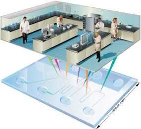
single credit-card sized chip (Figure 1.1). Microfluidics technology, utilizing the
manipulation of micro to nanoliter volumes of fluid, provides an avenue to such systems.
These so-called lab-on-chip systems are of significant interest to researchers for many
reasons including (i) reduced costs due to minute sample and reagent consumption, (ii)
improved sensitivity, (iii) shorter analysis times, (iv) simple operation by minimally
trained personnel, (v) portability, and (vi) disposability (Ng et al. 2010; Phillips and
Wellner 2007; Mauk et al. 2007). Lab-on-chip devices are often used as biosensors to
capture biological targets, such as proteins and nucleic acids, from a complex sample and
facilitate, among other things, medical diagnosis (e.g. HIV or malaria screening), food
and water quality inspection (e.g. bacterial contamination test), and environmental
monitoring (e.g. soil contamination test). All immunoassay procedures, including sample
introduction, antigen-antibody incubation, washing, labeling, and detection can be carried
out in an automated fashion in the microfluidic device. Thus, these devices offer
relatively sophisticated laboratory capabilities at the point-of-care, at home, and in
resource poor regions (Hart et al. 2011; Jokerst et al. 2010; Liu et al. 2009a; Linder
Polymeric materials are a popular choice for microfluidic devices because they
are inexpensive; amenable to various bonding techniques; exhibit good optical properties;
are machinable by a variety of methods such as milling, injection molding, and hot
embossing; facilitate monolithic production; and eliminate the need for packaging.
Polystyrene, polycarbonate, acrylic, polydimethylsiloxane (PDMS), and cyclic olefin
copolymer (COC) are several common chip materials. Among these, COC is particularly
advantageous due to its chemical stability, optical transparency, and low autofluorescence
(Laib and MacCraith 2007; Mair et al. 2006). Autofluorescence is unwanted background
fluorescence that can interfere with signal readings of captured analytes and adversely
affect limits of detection (Piruska et al. 2005). COC chips can be mass-produced by
Figure 1.1: A schematic depiction of the integration and miniaturization of laboratory
injection molding and/or hot embossing. For these reasons, we focus primarily on COC
substrates for chip fabrication in this dissertation.
To enable a biosensing test, a receptor capable of specifically binding the target
must be immobilized at a particular location inside the chip. In recent years, there has
been a growing interest in using spherical particles known as microbeads as a solid
support for capturing targets in both benchtop and microfluidic systems (Lim and Zhang
2007a; Verpoorte 2003; Qiu et al. 2009). Typically, the beads are polymeric (e.g.
polystyrene or agarose), porous or non-porous, range in size from a few micrometers to a
few hundred micrometers, and can be readily purchased with various surface
functionalizations such as oligonucleotides, antibodies, and antigens. Microbeads and
their incorporation as a biosensing platform in microfluidic chips is the primary focus of
this dissertation.
1.2 Microbeads in Biosensing
The integration of bead-based affinity assays into microfluidic chips is currently
an area of growing interest. Recent reviews by Ng et al. (2010) and Derveaux et al.
(2008) discuss the synergy between microbead and microfluidic technologies. As a
platform to capture targets, beads offer several advantages over planar configurations
including large surface areas to support biological interactions (increasing sensitivity),
the availability of a library of bead types from many vendors, and array-based formats
capable of detecting multiple targets simultaneously (multiplexing). For example, 1 g of
0.1 µm diameter beads has a total surface area of about 60 m2 (Verpoorte 2003).
solution can yield greater signal intensities than for the same reaction in solution. Thus
beads can improve detection limits by essentially amplifying the signal.
Due to their high throughput, sensitivity, and reduced assay times compared to
their macroscopic counterparts, bead-based microfluidic devices are especially vital in
providing rapid and accurate detection of disease biomarkers in point-of-care applications
(Jokerst et al. 2009; Derveaux et al. 2008). Several recent bead-based assay studies have
demonstrated this principle. Agarose microbeads localized in micromachined cavities on
a silicon wafer chip enabled simultaneous detection of cardiac risk factors C-reactive
protein and Interleukin-6 in human serum samples (Christodoulides et al. 2002), as well
as reduced DNA hybridization times from 4-12 hr to 5-40 min (Ali et al. 2003).
Antigen-antibody analysis times reduced from 24 hr to less than 1 hr to detect human secretory
immunoglobulin A (Sato et al. 2000), and from 45 hr to 35 min to detect
carcinoembryonic antigen (Sato et al. 2001) were achieved in a microchip using
antibody-coated polystyrene microbeads. Antigen-coated magnetic microbeads
immobilized on-chip allowed rapid and sensitive quantification of human serum
immunoglobulin G antibodies to Helicobacter pylori (Pereira et al. 2010).
A wide variety of substrate materials fabricated with various techniques are
capable of accommodating beads on-chip. For instance, wells, chambers, cavities, and
weirs are commonly made on glass substrates (Sato et al. 2002; Sivagnanam et al. 2008),
silicon wafers (Ali et al. 2003; Xu et al. 2008; Hashmi et al. 2005), and optical fibers
(Blicharz et al. 2009; Bowden et al. 2005; Ferguson et al. 2000) using photolithographic
and etching techniques, and on PDMS (Shin et al. 2007; Zhou et al. 2006; Jeong et al.
primarily on top-down fabrication steps, bottom-up or self-assembly methods of
fabrication have also been used in certain applications. For example, a uniform hexagonal
array of spherical microcavities was formed by incorporating condensed water droplets
into an elastomer film and allowing the water to evaporate leaving behind vented,
spherical cavities (Shojaei-Zadeh et al. 2009). Numerous types of ordered microwell
arrays have been created in various materials using monolayers of colloidal crystals (Li et
al. 2008). While novel, the above works describe the formation of wells in materials that
are infrequently used for point-of-care devices.
A number of patterning techniques enable precise positioning of beads on-chip.
Array (Ali et al. 2003; Zhou et al. 2006; Filipponi et al. 2009; Li et al. 2005;
Christodoulides et al. 2002) and packed bed (Shin et al. 2007; Jeong et al. 2008; Chung et
al. 2005) formats are often utilized to arrange beads in microfluidic devices. Tools such
as magnetic fields (Barbee and Huang 2008; Pamme 2006; Gijs 2004), electric fields
(Barbee et al. 2009; Rosenthal and Voldman 2005), and micropipettes (Liu et al. 2009b)
may assist in bead placement. In one embodiment with multiplexing capabilities,
differentially functionalized, encoded beads are randomly dispersed in an ordered
microwell array, enabling the simultaneous analysis of an assortment of biomolecules in
a single assay. The beads are encoded with a distinct brightness or color to allow for
individual identification. For example, such beads were distributed among wells etched in
fiber-optic substrates to detect DNA and inflammatory cytokines in saliva (Blicharz et al.
2009; Bowden et al. 2005; Ferguson et al. 2000); in silicon wafers for large-scale, rapid
blood group DNA typing (Hashmi et al. 2005; Stevens and Iwaki 2008); and in PDMS
antirabbit immunoglobulin G (Lim and Zhang 2007b). Microbeads with different
oligonucleotide probes for rapid DNA detection have also been randomly, sequentially
dispersed on gel pads comprised of an array of micropillars and their positions identified
following each dispersion step, thus, eliminating the need for coding (Ng et al. 2008).
A few studies have examined the binding kinetics of several types of
biomolecules to functionalized, micron-sized bead surfaces. These include the binding of
(i) biotinylated DNA (Fujita and Silver 1993; Huang et al. 1996) and fluorescein biotin
(Buranda et al. 1999) to streptavidin-coated beads, (ii) biotinylated horseradish
peroxidase to avidin-coated beads (Ku and Lentrichia 1989), (iii) glutathione
S-transferase (GST) to anti-GST antibody-coated beads (Sasuga et al. 2006), and (iv)
proteins to aptamer-coated beads (Kirby et al. 2004), as well as (v) the hybridization of
target DNA to complementary DNA immobilized on beads (Henry et al. 1999; Stevens et
al. 1999). Although good knowledge of bead binding kinetics is critical for effective
implementation of microbead technology, there are just a few systematic studies
addressing this issue (Verpoorte 2003).
Figure 1.2 depicts some of the primary research groups and companies
specializing in microbead-based biosensing technology. Dr. John McDevitt's group
(formerly at the University of Texas at Austin; currently at Rice University) developed
novel methods to construct agarose bead (~300 µm in diameter) arrays in a silicon wafer
containing pyramidal wells etched through its thickness (Figure 1.2a). LabNow, Inc.
(Austin, TX) commercialized McDevitt's technology in 2003 and remains a private
company specializing in providing accessible point-of-need solutions that improve global
(www.tastechip.com/www/labchip/lab _on_a_chip.html)
(www.illumina.com/technology/ beadarray_technology.ilmn)
(http://www.immucor.com/bioarray) (http://www.luminexcorp.com /technology/index.html)
a
b
c
d
(www.tastechip.com/www/labchip/lab _on_a_chip.html)
(www.illumina.com/technology/ beadarray_technology.ilmn)
(http://www.immucor.com/bioarray) (http://www.luminexcorp.com /technology/index.html)
a
b
c
d
Figure 1.2: Several existing platforms for microbead-based biosensing. (a) 300 µm
beads in a silicon wafer (Dr. John McDevitt's group; Rice University; LabNow, Inc.; "Nano-Bio-Chip"). (b) 3 µm beads in a silicon wafer or optical fiber bundle (Dr. David Walt's group; Tufts University; Illumina, Inc.; "BeadArray Technology"). (c) 3 µm beads in a silicon wafer (BioArray Solutions, An Immucor Company; "BeadChip"). (d) 5.6 µm beads with a flow cytometer (Luminex Corporation; "xMAP Technology").
randomly pattern encoded microbeads (~3 µm in diameter) on etched fiber optic bundles
and silicon wafers (Figure 1.2b). Illumina, Inc. (San Diego, CA) commercialized Walt's
technology in 1998and has grown rapidly since then by applying innovative technologies
to study genetic variation and function. Illumina publicly trades on the NASDAQ stock
exchange under the symbol ILMN. Another company, BioArray Solutions (Warren, NJ),
developed a technology similar to Walt's for randomly patterning encoded beads (~3 µm
in diameter) on silicon wafers (Figure 1.2c). BioArray Solutions was purchased by
Immucor, Inc. in 2008 and currently trades under the symbol BLUD. Luminex
Corporation (Austin, TX), incorporated in 1995, developed a flow cytometer, dual laser
based system to read emissions from beads (5.6 µm in diameter) with up to 100 unique
fluorescent signatures (Figure 1.2d). Luminex provides technology for rapid, sensitive,
cost-effective, and multiplexed bioassays and currently trades under the symbol LMNX.
1.3 Motivation for Research and Organization of Dissertation
Although microbeads are increasingly prevalent in microfluidic biosensors, and
good knowledge of mass transfer and binding kinetics in porous and non-porous beads is
critical for effective implementation of microbead technology, there is a fundamental lack
of studies in this area. We aim to address a host of key issues associated with integrating
microbeads on a chip. For example, (1) we are unaware of existing three-dimensional
computer models capable of predicting bead binding kinetics that have been verified
experimentally; (2) few existing biosensor designs are capable of directly integrating
microbead arrays of various sizes and assembly techniques into plastic devices; (3) the
coupling of the unique elastic and sponge-like nature of certain porous beads has not been
shelf life of bead-based chips; and (5) few studies examine the feasibility of using
portable, handheld devices to measure bead fluorescent emissions on a chip.
The motivation for this dissertation is therefore to conduct a comprehensive,
systematic investigation of microbead-based biosensing in microfluidic devices. The
novelty of this work will be demonstrated by developing a new set of experimental
devices and theoretical models to understand and advance the current state of bead-based
biosensing chips. The dissertation, following this introductory chapter (Chapter 1), is
organized as follows:
Chapter 2: Describes a method of integrating microwell arrays of various sizes directly in
a plastic substrate and assembling the substrate into a microfluidic chip.
Includes a discussion of autofluorescence and photobleaching issues that may
adversely impact chip performance.
Chapter 3: Describes a technique to selectively place beads within an array and perform
an affinity assay. Develops a theoretical model to predict mass transfer and
binding kinetics for an impermeable, non-porous bead.
Chapter 4: Describes a method to analyze binding for a permeable, porous bead using
confocal microscopy. Develops a theoretical model to predict mass transfer
and binding kinetics for a porous bead. Discusses the impact of bead
compression on test characteristics.
Chapter 5: Describes a method of controllable uniaxial bead pulsation to enhance binding
Chapter 6: Describes further characterization of the behavior of beads on a chip,
including shelf life studies and alternative measurement techniques with a
handheld reader.
Chapter 7: Describes techniques to incorporate randomly structured microbead arrays in
a pouch-based cassette and in a flow cell. Validates the biosensing capability
of each device using a bead-based immunoassay.
CHAPTER 2: Fabrication of Microwell Arrays in Plastic by Hot
Embossing and Assembly of Microfluidic Chip
2.1 Introduction
Hot embossing is a convenient and repeatable way to rapidly stamp micropatterns
in polymers using a prefabricated multiuse master (Becker and Heim 2000; Kimerling et
al. 2006). The process involves heating a master containing microfeatures to above the
softening temperature of the polymer, and then pressing the polymer against the master.
Once the micropattern on the master transfers to the plastic, pressure is relieved, and
typically both the master and polymer are allowed to cool to below the polymer softening
temperature before separating the two pieces. In this chapter, we first discuss the two
master fabrication techniques (plasma-etching and machining) we used to create an array
of micropins, and then describe our custom-built hot embossing setup used to stamp a
corresponding set of microwell arrays. To fabricate pins smaller and larger than
approximately 80 µm in diameter and 60 µm in depth, respectively, we used
photolithography of silicon and computer numerical control (CNC) machining of
aluminum. Next we describe how an embossed substrate containing a microwell array is
assembled into a microfluidic chip. The assembly process employs disposable materials,
is simple, and does not require sophisticated facilities. Finally we describe how two
issues, autofluorescence and photobleaching, can adversely impact the performance of
2.2 Fabrication of Silicon Stamping Masters from Photolithography
2.2.1 Formation of Large Diameter, Tall Pins
To emboss wells ~40-60 µm in depth to accommodate agarose beads (with greater
depth precision than could be achieved by CNC machining), a master containing a 2×2
array of protruding pins was fabricated in silicon using standard photolithography
techniques. Three layers of Microposit S1827 positive photoresist (Rohm and Haas,
Philadelphia, PA) were spun (25 sec at 2000 rpm) and then baked (2 min at 120 °C) on a
3-inch silicon wafer. The resist was patterned in a Karl Suss MA-4 mask aligner (SUSS
MicroTec Inc., Waterbury Center, VT) using a chrome/glass photomask (150 sec UV
exposure), and developed (~8 min) in Microposit MF319 Developer (Rohm and Haas,
Philadelphia, PA). Following a post-bake (120 °C for 7 hrs), with the resist serving as the
etch mask, the silicon was plasma-etched (200 W for 45 min) with a gas mixture of SF6
and O2 (PlanarEtch II plasma machine, Technics Inc., San Jose, CA) to form the pin
array. Finally the remaining resist was removed (10 min submersion) with Microposit
Remover 1165 resist stripper (Rohm and Haas, Philadelphia, PA).
2.2.2 Formation of Small Diameter, Short Pins
To emboss wells ~1-3 µm in depth to accommodate methylstyrene-based polymer
beads, a second type of master was fabricated in silicon using standard photolithography
techniques. The master contained two different square patterns: one with 15 µm spacing
between pin centers (pitch) and the other with 30 µm pitch. The size of the array, the
number of wells and the wells' sizes, shape, and pattern can vary to accommodate
particular needs. Microposit S1827 positive photoresist (Rohm and Haas) was coated on
MicroTec Inc.) using a chrome/glass photomask, and developed in Microposit MF319
Developer (Rohm and Haas). With the resist serving as the etch mask, the silicon was
plasma-etched (PlanarEtch II, Technics Inc.) to form the pin array using a gas mixture of
SF6 and O2. Finally, the remaining resist was removed using Microposit Remover 1165
resist stripper (Rohm and Haas).
The geometries of the silicon pin array, stamped wells, and bead-well interface
were imaged using an atomic force microscope (Dimension 3100, Digital Instruments,
Veeco Metrology Group, Santa Barbara, CA), a dual-beam focused ion beam scanning
electron microscope (Strata DB 235, FEI Company, Hillsboro, OR), and a field-emission
scanning electron microscope (Quanta 600 FEG Mark II ESEM, FEI Company).
2.3 Fabrication of Aluminum Stamping Masters from CNC Machining
To emboss wells deeper than ~60 µm in depth, masters were fabricated in
aluminum using a precision Haas Office Mill CNC machine (Haas Automation Inc.,
Oxnard, CA). Aluminum is inexpensive (~$20 for 12" × 12" × ¼" sheet), machines well,
and can be rapidly heated and cooled during embossing (Mecomber et al. 2005). The
master geometry was designed in SolidWorks (SolidWorks Corp., Concord, MA) and
machining tool paths were defined in SolidCAM (SolidCAM Ltd., Or-Yehuda, Israel).
These two software packages are specifically designed to work together, which allows for
seamless part updates and regeneration of the G-code, which is read line-by-line by the
CNC machine. Various microtools, for example a 75 µm diameter carbide end mill
(Harvey Tool Company, LLC, Rowley, MA), were used to cut a 2×2 array of cylindrical
pins (diameter: ~80 µm, depth: ~60 µm, center-to-center spacing: 250 µm). By planing
could be controlled quite accurately to within a tolerance of ± ~10 µm. The maximum
depth that can typically be achieved with these micro end mills is 1.5-3 times the
diameter of the tool. The smallest diameter end mill we used during fabrication was 50
µm. The tool feed rate was 0.5 inch min-1 around the pins and 1 inch min-1 away from the
pins with a spindle speed of 30,000 rpm.
2.4 Hot Embossing of Microwell Arrays in Plastic
2.4.1 Embossing of Large Diameter, Tall Pins with Silicon Master
Following fabrication, the master was epoxy-bonded to a small aluminum block
to increase its rigidity and prevent fracture during embossing. A custom-built embossing
setup (Figure 2.1) was made by placing the master and COC substrate on a small hotplate
(Isotemp, Fisher Scientific, Pittsburgh, PA) mounted under an upright, vertical
microscope stage. The setup consisted of components that could readily be found in most
scientific laboratories, avoiding the need to specially purchase a hot embossing machine.
Figure 2.1: Custom-fabricated hot embossing setup to stamp a microbead array. The
plastic substrate is lowered and pressed against the heated master using the knob on the vertical stage.
hotplate
master substrate vertical
stage
hotplate
master substrate vertical
Furthermore, the setup's small footprint (~1 cubic foot) rendered it easily transportable,
with an assembly time of less than 1 min at a desired location. The microscope's
objectives were removed and replaced with a flat block of aluminum that served as an
upper stamping surface. Downward pressure (enough to slightly compress the rubber feet
on the hotplate) was applied at an embossing temperature of 200 ºC for 1-2 sec by turning
the knob mounted on the stage and lowering the head to the heated surface. After
stamping, the master and substrate were removed from the hotplate and allowed to cool at
room temperature. Figure 2.2a is a Scanning Electron Microscope (SEM) image showing
the master etched in silicon. The pitch of the array was 250 ± 0.6 µm. The pins were 44 ±
1 µm tall, and the pin's diameter varied from approximately 60 µm at the top to 80 µm at
the base as a result of the etching process. Figure 2.2b depicts the corresponding wells
hot embossed in COC. The wells were tapered, and they ranged in diameter from 60
(bottom) to 80 (top) ± 2 µm and had a depth of 44 ± 4 µm. The tolerance of the distance
between the well centers was a fraction of a micron.
2.4.2 Embossing of Small Diameter, Short Pins with Silicon Master
Following fabrication, the master was epoxy-bonded to a small aluminum block
to increase the master's rigidity and prevent fracture during embossing. The custom-built
embossing setup utilized here was similar to that described above. Briefly, the master was
placed on a small hotplate (Isotemp, Fisher Scientific, Pittsburgh, PA) mounted beneath
an upright vertical microscope stage. The microscope's objectives were removed and
replaced with a flat block of aluminum containing a row of three mounting pillars. The
COC substrate was fixed to the two outside pillars with double-sided tape, and the middle
a
b
a
b
a
b
a
b
Figure 2.2: (a) Electron micrograph of stamping master with large pins etched in
silicon. (b) Corresponding wells hot embossed in COC.
Figure 2.3: (a) Electron micrograph of stamping master with small pins etched in
compress the rubber feet on the hotplate) was applied at an embossing temperature of 200
ºC for 1-2 sec by turning the knob mounted on the stage and lowering the head to the
heated surface. Following stamping, the head was lifted and the substrate was removed
from the pillars. We did not need to treat the surface of the master to avoid sticking to the
substrate. Although we focus on COC substrates in this thesis, we have also hot
embossed wells in other plastics such as polycarbonate.
An important advantage of our system is the ability to rapidly, repeatedly, and
consistently stamp well arrays in a plastic substrate. Figure 2.3a shows a portion of the
master (15 µm pitch) etched in silicon after embossing approximately 30 arrays. The
tapered, circular pins were 1.8 µm tall, and, as a result of the etching process, their
diameter varied from approximately 3.7 µm at the top to 5.1 µm at the base. Figure 2.3b
shows the corresponding wells hot embossed in COC. The pattern from the silicon master
precisely transferred to the plastic, and the tapered wells ranged in diameter from 3.7
(bottom) to 5.1 (top) ± 0.1 µm and had a depth of 1.8 ± 0.05 µm, as measured with an
atomic force microscope. The tolerance of the distance between the well centers was
approximately 0.25 µm. Tolerances were established by measuring multiple wells from
several different arrays, illustrating that the geometry of the pins remained in near pristine
condition after repeated use. The time required to stamp each array was approximately 1
min, an attribute made possible because the master remains on the hotplate at constant
temperature during repetitive stamping, and only the microscope head (containing the
plastic substrate) is raised and lowered from the heated surface. This is an improvement
over Section 2.4.1, where both the substrate and master were removed from the hotplate
2.4.3 Embossing of Large Diameter, Tall Pins with Aluminum Master
Figure 2.4a shows a master containing a 2×2 array of CNC-machined pins at the
center of the aluminum. Tool marks produced by the end mill during machining are
visible at the base of the pins. Figure 2.4b shows the corresponding wells hot embossed
in COC. The master remained in good condition after stamping over 40 plastic
substrates. While microwells embossed from aluminum masters were sufficient for a
variety of preliminary bead placement experiments, the ability of silicon microfabrication
to produce more accurate microfeatures made silicon wafer patterning the desired
technique for microwell array formation.
2.5 Assembly of Microfluidic Chip
The microfluidic chip (Figure 2.5) consisted of three layers: a bottom 100 µm
thick COC substrate (Plitek, Des Plaines, IL) containing the embossed microwell array; a
central double-sided adhesive tape with a conduit cut in its center with a laser machine;
Figure 2.4: (a) Electron micrograph of CNC-machined aluminum stamping master
after embossing ~40 substrates. (b) Corresponding wells hot embossed in COC.
a
b
and a top 100 µm thick COC cover (Plitek). The adhesive tape acted as a spacer, dictating
the height of the conduit, as well as a sealing material. We used 50 µm (Carolina Tape
and Supply Corporation, Hickory, NC) and 75 µm (Tape-Rite Co. Inc., New Hyde Park,
NY) thick tapes for our experiments.The COC cover contained inlet and outlet ports. The
wells could be populated with beads either selectively (Figure 2.5a) or randomly (Figure
2.5b), as described in Chapters 3 and 7, respectively. Thin top and bottom substrates were
chosen for the device to minimize background fluorescence, which decreases as the
thickness of the plastic decreases (Hawkins and Yager 2003) and is discussed in the next
section. The parts for multiple chips (substrate and conduit) were fabricated
simultaneously with a laser cutter (X-660, Universal Laser Systems, Scottsdale, AZ),
requiring less than 1 min per chip. A slightly tapered conduit was cut in the adhesive
membrane to form a flow channel, since we observed in the experiments that the taper
minimized entrapment of air bubbles as compared to a straight conduit. After the
membrane was bonded to the base substrate containing the microbead array, the top of
the channel was sealed with a second piece of COC containing a sample inlet port. Inlet
Figure 2.5: (a) A schematic depiction of the experimental chip containing the
controllably assembled microbead array (4 beads are shown). (b) The same chip containing the randomly assembled microbead array (2 bead types are shown).
Controllably Assembled Microbead Array Reagent Flow
a
Conduit Inlet 50 mm 12 mm Randomly Assembled Microbead Arrayb
50 µm tall
Controllably Assembled Microbead Array Reagent Flow
a
Conduit Inlet 50 mm 12 mm Randomly Assembled Microbead Arrayb
50 µm tall
50 mm 12 mm Randomly Assembled Microbead Array
b
tubing was fixed in place with a small PDMS block and connected to a programmable
syringe pump (PHD 2000, Harvard Apparatus, Holliston, MA). In some experiments, the
PDMS block contained a trap (optional; not shown) to prevent any air bubbles arising
from interchanging reagent syringes from entering the chamber. Reagents exiting the chip
were absorbed with a Kimwipe (Kimberly-Clark Corporation, Neenah, WI) or collected
with an optional outlet tube and drain.
2.6 Autofluorescence and Photobleaching in Bead-Based Microfluidic Chips
With the prevalence of lab-on-chips in biotechnology today, it is important to
understand the material properties of these devices and identify some of the common
issues that arise when performing affinity assays. Two issues that can influence
experimental results in lab-on-chip devices are autofluorescence and photobleaching.
Autofluorescence is undesirable background fluorescence that interferes with on-chip
optical measurements and often leads to suboptimal limits of detection. The roots of
autofluorescence are varied, from additives routinely added to commercial polymers, to
particular reagents used to functionalize the surface of a microbead (Piruska et al. 2005;
Mair et al. 2006). Autofluorescence varies among different polymers and decreases as the
thickness of the substrate decreases because a lesser volume of material is being
illuminated (Hawkins and Yager 2003). Photobleaching occurs when a fluorophore loses
its ability to emit light due to photon-induced chemical damage. The underlying
mechanisms for photobleaching are not well understood, but the degree of bleaching is
dependent on the intensity and duration of exposure of the incident light (Herman et al.
2006). As demonstrated below, photobleaching can sometimes be intentionally exploited
Controlling autofluorescence and photobleaching issues when they arise in
microfluidic devices is critical to obtain satisfactory imaging data. In our experiments,
these issues were first encountered when monitoring the binding of biotin-coated
quantum dots (biotin-QDot605, emission maximum at 605 nm, Invitrogen, Carlsbad, CA)
to 90 µm diameter streptavidin-coated polystyrene beads (Spherotech Inc., Libertyville,
IL). The streptavidin-coated polystyrene beads exhibited a significant autofluorescence.
Based on a personal communication with a representative of the bead manufacturer, the
autofluorescence is likely due to the addition of a functional group that is needed to
covalently couple the streptavidin to the polystyrene carboxyl derivative resin
(Kildew-Shah 2007). Other groups have also observed this phenomenon with streptavidin-coated
beads (Hinz et al. 2001; Ng et al. 2008). With this knowledge at hand, we did still
perform some preliminary experiments by incubating biotin-QDots with
streptavidin-coated polystyrene beads resting in a well. The early portion of a binding curve with a 1
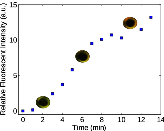
nM QDot concentration is shown in Figure 2.6. Images were acquired with an
epifluorescence microscope (BX51, Olympus Corporation, Melville, NY) with a long
pass filter (ex: 470 nm, em: > 515 nm, filter set 11001v2, Chroma Technology
Corporation, Rockingham, VT) and a color CCD video camera system (Optronics,
Goleta, CA). Fluorescent micrographs of a single bead at 2, 6, and 11 min are included to
show how initial bead autofluorescence (green) decreases simultaneously as more QDots
(orange) bind to the surface of the bead. Figure 2.6 demonstrates that for the duration of
this short experiment, the bead surface is only partially covered with bound QDots.
We performed experiments to monitor the autofluorescence decay of
Figure 2.6: Experimental binding curve using streptavidin-coated polystyrene beads
and 1 nM biotin-QDot605 solution. Relative fluorescent intensity of the bead (Ib) is defined in arbitrary units (a.u.) as Ib(t) - Ib(t = 0). The initial autofluorescence of the beads (green) decreases simultaneously as more QDots (orange) bind to the surface of the bead.
Figure 2.7: Autofluorescence decay of streptavidin-coated polystyrene beads under
continuous illumination from an epifluorescence microscope. (a) Absolute fluorescent intensity of well-immobilized beads and COC substrate. (b) Plot in (a) normalized by the maximum fluorescent intensity of each bead.
0 2 4 6 8 10 12 14
0 5 10 15 Time (min) R e la ti v e F lu o re s c e n t In te n s it y ( a .u .)
0 2 4 6 8 10 12 14
0 5 10 15 Time (min) R e la ti v e F lu o re s c e n t In te n s it y ( a .u .)
0 20 40 60
0 0.2 0.4 0.6 0.8 1 Time (min) F lu o re s c e n t In te n s it y ( a .u
.) Bead 1Bead 2
Bead 3
0 20 40 60
0 50 100 150 200 Time (min) F lu o re s c e n t In te n s it y ( a .u
.) Bead 1Bead 2
Bead 3 Substrate
a
b
0 20 40 60
0 0.2 0.4 0.6 0.8 1 Time (min) F lu o re s c e n t In te n s it y ( a .u
.) Bead 1Bead 2
Bead 3
0 20 40 60
0 50 100 150 200 Time (min) F lu o re s c e n t In te n s it y ( a .u
.) Bead 1Bead 2
Bead 3 Substrate
on the microscope. The results for three beads for 60 min of illumination are shown in
Figure 2.7. The autofluorescence of the beads is being destroyed through photobleaching
as illumination continues. Figure 2.7a illustrates how bead autofluorescence is initially
much brighter, and decays more quickly, than the background emission of the COC
polymer substrate. Figure 2.7b, where bead intensity values were normalized by their
value at t = 0, demonstrates that beads with initially different autofluorescence intensities
follow similar decay rates when continually exposed to incident photons. Although these
experiments helped quantify the rate of the autofluorescence decay, it was still difficult to
accurately resolve signal fluorescence (emitted from bound QDots) from background
fluorescence (emitted from bead autofluorescence). For this reason, we early on switched
from streptavidin-coated polystyrene beads to streptavidin-coated agarose beads (Pierce
Biotechnology, Rockford, IL) because the agarose beads did not exhibit this inherent
autofluorescence problem.
Although the streptavidin-agarose beads did not inherently autofluoresce like the
polystyrene, the functionalized agarose was not completely void of fluorescence issues
under certain circumstances. In an attempt to photobleach any autofluorescence from the
COC substrate, and because QDots do not photobleach, the shutter on the microscope
was left open for an entire preliminary binding experiment, allowing continual filtered
light to shine on the beads and substrate. This resulted in the development, and
subsequent increase, of autofluorescence in the streptavidin-agarose beads, which was
originally mistaken to be QDots binding to the bead. The mechanism for this undesirable
observation is still unclear, but may be due to temperature effects resulting from the
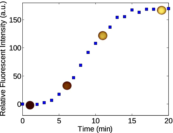
An experiment with streptavidin-agarose beads demonstrating this phenomenon is
shown in Figure 2.8. The substrate for the experiment contained 100 µm diameter wells
hot embossed in a 250 µm thick piece of COC. Fluorescent images were acquired as
described previously. Although it appears that the surface of the bead becomes saturated
with QDots after about 15 min, the increase in fluorescent intensity was due to
autofluorescence resulting from continuous illumination. This was verified because (i)
the fluorescence occurred for all emission wavelengths (the QDots only emit at 605 nm);
(ii) it occurred even for a buffer solution containing no QDots, so the surface of the bead
could not possibly be saturated with label; (iii) the intensity of the entire bead increased
uniformly with time in Figure 2.8, as opposed to actual specific binding of the QDots,
0 5 10 15 20
0 50 100 150 Time (min) R e la ti v e F lu o re s c e n t In te n s it y ( a .u .)
0 5 10 15 20
0 50 100 150 Time (min) R e la ti v e F lu o re s c e n t In te n s it y ( a .u .)
Figure 2.8: Increased autofluorescence of high capacity streptavidin-coated agarose
where a bright ring starts at the periphery of the porous bead and proceeds toward the
center of the bead as binding continues; and (iv) real equilibrium required much longer
than 15 min (Chapters 3-5).
We applied the early lessons of this section to our subsequent experiments in
Chapters 3-7. In summary, these lessons are: (1) the autofluorescence of plastic substrates
can be reduced by decreasing the thickness of the substrate; (2) when choosing a
fluorophore or label reporter for an affinity assay, be mindful of incident light exposure
potentially inducing photobleaching; (3) when selecting functionalized microbeads for an
affinity assay, generally avoid beads that exhibit autofluorescence properties which may
interfere with fluorescent reporting; and (4) exposing beads and reporters to a minimum
amount of incident light (i.e., only opening the microscope's shutter when acquiring a
data point) usually reduces complications due to autofluorescence and photobleaching.
2.7 Conclusions
We used photolithographic microfabrication and CNC machining, respectively, to
generate micropin arrays in silicon and aluminum. The size of the pins and the array can
be tailored for individual needs and applications. We devised a customized hot
embossing setup employing readily available laboratory materials to directly stamp
microwell arrays in a plastic substrate. Direct fabrication of the uniform wells within the
conduit material, avoiding the need to interface with silicon or other components, is
likely to reduce the device's cost and complexity. The embossing process is rapid,
repeatable, and enables the wells to be loaded with beads using controllable (Chapters
3-4) or random (Chapter 7) techniques. We developed a microfluidic chip utilizing a
loaded array into a flow cell. The height of the conduit is easily controlled by adjusting
the thickness of the sealing tape. The forces immobilizing the beads in place in the array
during fluid flow are described in subsequent chapters. Overall, the entire chip fabrication
process is relatively simple and does not require sophisticated facilities. Finally, in this
chapter we described autofluorescence and photobleaching phenomena that may be
encountered in bead-based microfluidic chips, but can be overcome by an informed
CHAPTER 3: Non-Porous Microbead Affinity Assay: Experiments and
Finite Element Simulations
3.1 Introduction
Agarose beads are a common support for protein detection, DNA hybridization,
and affinity chromatography (Jokerst et al. 2011; Christodoulides et al. 2005; Ali et al.
2003; Ogata et al. 2002; Horstmann et al. 1986). As opposed to random assembly, where
beads randomly fill wells and an encoding step is necessary to identify the location of
each bead type (Ferguson et al. 2000; Ng et al. 2008; Bowden et al. 2005), here we
capture a bead of known functionalization with a micropipette, maneuver the
micropipette with a micromanipulator, and place the bead in a designated well. This
process is amenable to automation (Sohn et al. 2005). The 2×2 array of agarose beads is
contained within a single-use (disposable) microfluidic flow cell.
For our experiments, we used a model system comprised of a biotinylated
fluorescent label and streptavidin-coated agarose beads. The biotin-streptavidin system
was selected because of its simplicity and frequent use in bead-based assays (Ng et al.
2007; Kim et al. 2006; Wen et al. 2007). The experimental concepts, however, are also
applicable to other biological systems such as sandwich assays for antigen-antibody
interactions (Qian and Bau 2003). In the array, we used "test" beads covalently
conjugated with the tetrameric protein streptavidin (MW = 52,800 Da). Streptavidin
binds very tightly to the vitamin biotin (MW = 244 Da). As a result, streptavidin-biotin
linkages are routinely employed in many biosensing assays. As the model target analyte,
we used biotin-conjugated quantum dots (10-12 nm in diameter). Quantum dots are
photobleaching, and are often used in microbead assays (Zhang et al. 2010; Han et al.
2001; Gao and Nie 2004; Yun et al. 2006; Riegger et al. 2006; Agrawal et al. 2007). To
assess undesirable, non-specific binding of the target analyte to the agarose matrix,
several control tests were performed with plain agarose "control" beads.
To further understand our miniaturized microbead system, we performed
three-dimensional numerical simulations to model the binding of analyte to a bead immobilized
in a microfluidic channel. Although several prior modeling studies of heterogeneous
microfluidic assays examined the effect of channel geometry, flow rate, binding rate
constants, concentration, and volume and time constraints on analyte capture efficiency
(Myszka et al. 1998; Vijayendran et al. 1999; Zimmermann et al. 2005; Hu et al. 2007;
Parsa et al. 2008), they dealt with planar geometries and were restricted to two
dimensions. This simplification is not appropriate for three-dimensional, immobilized
bead systems.
3.2 Experiments
Experiments were first conducted to examine the material behavior of the
polydisperse agarose beads (wet diameter range of 27-200 µm with average diameter of
~90 µm (Xue and Sun 2003); 6% mass fraction crosslinked agarose support from Pierce
Biotechnology, Rockford, IL) during drying and rehydration. 100 µL of stock
streptavidin-agarose beads were washed tenfold and resuspended in 100 µ L of deionized
water. Several microliters of solution were then serially diluted to a working
concentration of approximately 10-20 beads per microliter. A drop was pipetted onto a
glass microscope slide pre-cleaned with isopropanol. The initial hydrated diameter of
objective). The beads were then continuously monitored while the liquid in the drop
evaporated at room temperature. Once the beads had dried, their diameter was again
measured. Finally the beads were rehydrated with a 1 µ L drop of deionized water and
their recovered diameter was tabulated. This process was repeated several times for
multiple beads of different initial diameters. Results demonstrate that upon drying the
diameter of the bead decreased by 60% ± 2% (e.g. a wet bead of 100 µm diameter shrank
to ~40 µm upon drying at room temperature), and after rehydration the bead returned to
its initial size (negligible hysteresis). These results were independent of bead size, which
implies that the agarose bead's mass fraction (6%) and not its initial diameter is the
important factor during repeated drying cycles.
Upon understanding the beads' drying and rehydration behavior, to install the
beads in the chip, a 5 µL aliquot of streptavidin-agarose beads was diluted twofold with
deionized water and allowed to dry at room temperature. In some experiments, plain 6%
agarose beads (Sepharose CL-6B, Sigma-Aldrich, St. Louis, MO) were also implemented
as a control. Subsequently, under magnification, appropriately sized dry beads were
selected (~50 µm diameter) and placed in the wells using a micropipette and
micromanipulator (MMN-1, Narishige, Tokyo, Japan). The size of the dry bead was
chosen so that the top of the bead only slightly protruded above the top of the well, which
prevented the bead from being disturbed when sealing the flow cell with a second piece
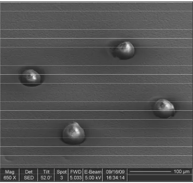
of 100 µm thick COC containing inlet and outlet ports. Figure 3.1 is a SEM image (650x
magnification) showing the array populated with four dry agarose beads.
At the start of an experiment, quantum dot solution (biotin-QDot605, emission