Development Of Co Gas Sensing Based SnO
2
Thin Film
I DewaPutuHermida
*), Yuyu R. Tayubi
**), Rani Nopriyanti
**)Abstract
--
This research, have done design and fabrication CO gas sensing based on SnO2 thin film by sol gel method. Forcomponent of gas sensing such as electrode was made of gold by sputtering and heater was made of PdAg by screen printing. S o that, sensor is expected to yields high sensitivity. Tests on sensors is conducted to determine the effect of temperature on the resistance of the sensor and the sensitivity of the sensor with a given flow rate of 10 ppm CO gas. The effect that occur in the sensor gas that when the temperature that given to sensor is enlarged then the sensitivity will increase as well, but when the temperature is given to sensor through its operational temperature sensor, the sensitivity of sensor value will decrease. It also conducted tests using S EM and EDS to determine the morphology and composition of the constituent sensor. Thus shown that the coating formed sensor has 21.21% C atoms, 22.43% O atoms, 14.98% Si atoms, 0.34% Cr atoms, 1.16% Ag atoms, 1.78% S n atoms, and 38.11% Au atoms. Operational temperature owned by this sensor is 95° C with the highest sensitivity value of this sensor is 16.59.
Index Term--
S nO2, CO gas sensing, sensitivity, sputtering.1. INT RODUCT ION
Carbon mono xide (CO) is a gas that is fla mmable, poisonous, colorless, and tasteless. Because of it is not colored and tasteless carbon mono xide is difficult to detect when without using detection technology [1]. Therefore , carbon mono xide is often dubbed the "silent killer", and needed a technology that can detect the presence of CO gas.
Science and technology of the se miconductor gas sensor was growing rapid ly. Device semiconductors gas sensor are generally known as a metal o xide gas sensor because it is made of metal o xides such as TiO2, Zn O, CeO2 and SnO2 [2].
Among all the meta l o xide, Sn O2 is one material that is good enough to be used as the active layer of CO gas sensors [3]. Nevertheless, SnO2-based gas sensor to date has not made the high sensitivity and selectivity. [4]. According to Pires, one of the factors that can improve the quality of a sensor that is optimizing the quality of the electrode. Electrodes used in a sensor must have high conductivity values. In order fo r the resulting e lectrode has a good quality, the electrodes can be fabricated using thin-film technology and made using materia ls that have good electrical conductivity [5].
Along with the development of mic roelectronics technology or nanotechnology at this time, electrode fabrication technology that is applied to metal o xide-based gas sensors can be done using the method sputtering. Using Sputtering technology of thin film gro wth becomes simple r and operational costs become cheaper. In addition, by using the method of Sputtering adhesives between the coating and the substrate surface becomes stronger, coating thickness easily observed and controlled [6].
The purpose of this research is to determine the characterizat ion of SnO2-based CO gas sensors has been done in terms of the development of electrode components.
2. EXPERIMENT AL
2.1. Design of Gas Sensor
Parts of Sensor
Gas sensor is composed of electrodes that coated by a layer. And the layer is sensitive to the presence of CO gas sensors are printed on a substrate of silicon (Si). Heater sensor printed on the subtrate surface alumina (Al2O3). Here's a specifications of gas sensor CO:
Dimensions : ≤10 mmx25 mm
Researching Power of Heater : 1.8 Watt
Operating temperature : 25-250o C
Measurement Range : 0 ~ 10ppm
Voltage Sensor : 3 volt dc
Heater Voltage : 3 volt dc
Designing of Eectrode
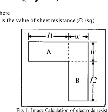
The electrodes are co mmon ly used in gas sensor components are generally an interdig ital e lectrode structure (interdig ital e lectrodes), wh ich are usually made of materials such as Au or Pt nobel meta l. The use of the structure was based on the consideration to minimize space but ma ximize the sensing area. To calcu late the value of the electrode resistance can be seen in the equation and the picture below:
( ) (1)
Where
Rs is the value of sheet resistance (Ω /sq).
Fig. 1. Image Calculation of electrode resistance value.
Pre-Bake
Coating of Resis
Soft Bake
Exposure
Development
Post Bake
Etsa
Cleaning Process Fig. 2. Design of Electrode
Design of Heater
One of the factors that determine the success of thin film gas sensors that are temperature factors that determine the success of thin film gas sensors that is te mperature. Appropriate temperature distribution will affect the level o f selectivity and sensitivity of this sensor element. To determine the characteristics of the heater, the para meters that must be considered are : the desired te mperature, the power needed, and the area that you want to heat the area, as well as the character o f the material heater itself (TCR, dissipation ma ximu m current that can pass through, etc. ). Thus the characteristics of the sensor heater is designed for:
Operating Temperature : 300oC
Average power : 1.8 Watts
Flow : 0.612 A
Based on the calculations that have been carried out, the heater has a length of line conductivity sensor of 94.107 mm and a track width of 0.529 mm. Then the resulting layout design heating gas sensor is as shown below:
Fig. 3. Heater of Gas Sensor Layout Design
3. SENSOR FABRICAT ION PROCESSE S
SnO2 gas sensor fabrication process is divided into three phases; there are the electrodes fabrication, heater fabrication, and the active layer fabrication. Here is the e xposure steps research that has been conducted by the author in several stages of research as follows:
3.1. Electrodes fabrication
The electrodes used in gas sensors, fabricated using sputtering method. Broadly speaking electrode fabrication steps illustrated in the diagram below:
Fig. 4. Electrode Fabrication Process
The first steps in the fabrication of electrodes is to do the washing substrate using acetone, 5% HF solution, DI Water and H2O2 solution: HCL:H2O. After that was done the process of oxidation. Th is research used dry oxidation process at a temperature of 1100OC for 130 minutes. Then later, the growth of Au thin films on silicon substrates using by DC Sputtering method and the pressure within the chamber to 5.9 x10⁻⁵ Torr and argon gas flowed at a pressure of about 4mTorr ± 0.1 mTorr. Be fore coated with gold, the substrate was coated with chro miu m first. Chro miu m coating was done for 2 minutes, which is then immediately followed by a coat of gold for 10 minutes.
Then to form the electrode pattern on a silicon substrate performed lithography process consists of several stages.
Fig. 5. Lithography process.
In the prebake process substrates in an oven at a temperature o f 85OC for 3 minutes in the oven. Immed iately after comp letion oven substrate, the substrate is coated resistors ma-P215 positive resist using a spin coater. Then do the soft bake process carried out in an oven with a temperature of 150OC for 15 minutes.
Printing design sensor
components into form ortho films
Preparation Tools and Materials
Cleaning of Substrate
Oxidation Gold
deposition (Sputtering)
lithography
Then do the process of exposure for 2 minutes in the sun and continued with the process of development by using MF319 developer solution until the pattern eme rges and then wash with DI Water. Then, the substrate reheat in the oven for 5 minutes with a te mperature of 85OC. Further etching process using a solution of I2:KI:H2O with a ratio o f 1:4:40 until golden patterns emerge, then wash with DI Water and dry. And then remove a layer of the re ma ining positive resist using acetone.
And the last thing to do in making the cutting was electrode substrate. The process of cutting the substrates used in this study was done manually using diamond eyes.
3.2. Making Sensor Heater
Heaters were made using thick-film technology and screen printing methods. In the making, to produce heater must pass through several processes including washing the substrate, making the screen, thick film gro wth, drying and burning. The substrate used in the fabrication of heater was alu mina substrate. Before use the substrate, it must be washed first by soaking in a glass beaker containing water dye, then put in the Ultrasonic cleaner for 5 minutes.
Furthermore, the first step that must be done in this process was the selection screen. In this study, used 325 mesh screen density and size 20 x 20 c m. After determining the screen to be used, the next thing to do is c lean the screen by using Ulano 5.
Then after the screen is co mplete ly dry, CDF3 film paper that has been cut into a size of 10 x 10 c m is placed in the midd le on the front surface of the screen. CDF 3 placed over the screen with the e mu ls ion at the top, and a little duct tape glue on one side of CDF 3 that were not easily moved. Then on the back surface of the screen was coated Ulano 133, just behind the CDF layer 3. Re move the masking tape that attached to one side of CDF 3, then dry it with a hair dryer for 15 minutes.
After Ulano 133 co mpletely dry, a layer of p lastic / my lar on CDF 3 re moved carefu lly . Furthermore, ortho-film paste on the upper right that has been released CDF 3 plastic coating. Then the screen was placed in the middle o f the fie ld of radiation on the radiation mach ine, the process was called by photography.
And the last one was on the screen that has not been covered by the CDF 3 coated again with a flattened Ulano 133 using rake l and dried using a hair dryer. After the pattern was formed on the screen, then performed the process of growing a thic k film on a lu mina substrate using screen printing and pastes used the pasta PdAg (Dupont 7484) to the value of the sheet resistance 15-30 mΩ/. Furthermore heater dried using an oven for 15 minutes at 195OC te mperature used. After heater beco ming d ry, the heater should be firing in a high tempe rature furnace. The length of time firing for about 30 minutes.
After the heater is formed, then cut to the size of the alu mina substrate heater is formed. Cutting substrate performed using diamond eyes.
3.3. Synthesis Procedures
First, we should prepare materials that will be us is powder SnCl, isopropanol, propanol and water. Comparison of the composition of the materials
to be used are powder SnO2: Isopropanol: Propanol: Water is 5: 7: 7: 6.
Fig. 6. SnCl powder
And then, puree SnO2 powder using a mortar and Pestle for ± 1 hour without stopping. This is done so that the particle size of SnO2 become nanoscale.Co mbine SnO2 powder that has been mashed with 2/3 parts of propanol and 1/3 water, then stir for 1 hour wh ile heated at a temperature of 80oC.
Burn the solution that has been made in the oven with a temperature of 300oC. After this stage, the solution will turn into powder.Co mb ine re main ing water, isopropanol and residual of propanol and powder. And then stir for 1 hour without heating, until resulting paste clear and homogeneous.Of the whole p rocess can be generated with sol-gel, then will be used to make a sensitive layer.
Fig. 7. SnO2 paste
Furthermore, to form a sensitive layer, SnO2 paste which was formed dripped right over the e lectrode which then leveled using a squeege.In order to coat the pasta in the electrode e xcept for the contact, then before coated the SnO2 contact parts should be covered by using solatip first.After the paste dries then the tape is opened.
4. RESULT S AND DISCUSSION
4.1. Micr o Str ucture and Structure Analysis by S EM-EDS
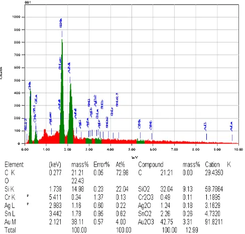
Fig. 8. EDS result gas sensor
Based on the fig. 12, it was observed that the ele ments contained in the SnO2-based CO gas sensors have the atomic co mposition of 21.21% C, 22.43% O atom, 14.98% Si, 0.34% Cr atoms, 1.16% atom Ag, 1.78% Sn atoms, and 38.11% Au atoms. The nu mber o f C ato ms in the sensor was obtained when the combustion process and testing using CO gas sensor, while the O ato ms derived from the absorption of free air.
While for the microstructure of the sensitive layer on a silicon substrate to deposition characterized using SEM . The results of the measurements in the form of SEM photographs shown in Fig. 8.
Fig. 9. Micro structure of SnO2 Thin Films with a magnification of 40000X
Fro m the SEM results above shows that the grain size of the Sn O2 thin film has reached the orde r of nano, but it can also be seen that the number of pores formed in the sensitive layer. This means, SnO2 thin layer formed qualify as gas sensors. Because, the gas sensor formed pores that capture of CO gas, which will then lowe r the resistance value and increases sensor sensitivity.
Based on the fig. 11 above, could be seen the thic kness of each material coated on a silicon substrate. Fig. 11 shows the micro structure of Sn O2 layer with a thic kness of 0.118 μm, Au (gold) with a thickness of 0.379 μm, Cr (Chro miu m) with 0.508 μm thickness, SiO2 (Silicon Dio xide) with 18.288 μm thick, while the Si (silicon) 39.03 μm.
4.2. Testing of Sensor
Test electrical characteristics init ially conducted under 0 ppm CO gas in other words without the granting of CO gas. Testing was done by changing the value of current supplied to the heater, which then change the value of a given temperature gas sensors. Along with the change in the value of the test temperature, then the value will change the resistance.
Then, the test continued with the characteristics of the gas flow rate of 10 ppm CO gas.Fro m the test results obtained can be seen in Fig. 11.
Fig. 10. T ransverse cross section of SnO2-Based CO Gas Sensor
Fig. 11. Chart Changes of Resistance Against T emperature Operations Sensor When Given and Without Gas CO
Based on the graph above, it can be seen that the gas sensor resistance decreases exponentially with increasing operating temperature is given, either when given only when given gas CO or CO gas. This is in accordance with the following equation :
(
) Description:
• R is the resistance at temperature measurement
SnO
2SnO
2• Ro is the resistance at the initial temperature measurement • Ea is the activation energy.
But the decline in the value of the resistance that occurs when no CO gas were not as decrease the resistance value when given gas. According to Andrew et. al. in 1999, it was because the normal a ir condition and heated sensor, there will be a process adsorbs oxygen fro m the a ir around to the surface gas sensors through grain boundaries. The oxygen has been adsorbed on the surface of the gas sensor will attract electrons fro m the conduction band of an n -type semiconductor gas sensor to the surface, so that the oxygen - oxygen is ionized into ions - oxygen ions O-,.
Thus, it resulted in the potential barrie r height (barrier between grains) will be high an d hinder the move ment of the e lectrons flowing through the grain boundaries. Then decrease the resistance value is not as big on testing for impa irment testing resistance at the same time but fed CO gas.
When compared to the results of the resistance obtained when no CO gas with CO gas is given, can be seen at a temperature of 60-140oC impairment resistance occurs when CO gas we re greater than without CO gas. This is due, when the CO gas flow into the heating chamber sensors re main to be done. In this situation, the reaction between CO gas with the gas sensor surface is:
2CO+2O- 2CO2 + 2e-
However, given the testing conditions with gas sensor irregularities. Deviations can be seen when the temperature reaches 200oC and 225oC, the temperature increased resistivity values. According to Khalil et a l In 2009, it was caused by the amount of carbon monoxide adsorbed gas mo lecules and accumulation of gas molecules occurs akibanya surface. Thus inhibiting the subsequent adsorption of carbon monoxide gas molecules.
Fro m the test results can also be obtained by the value of the sensor sensitivity. Fro m the data obtained a graph as shown in Fig. 12.
20 40 60 80 100 120 140 -2
0 2 4 6 8 10 12 14 16 18
S
e
n
s
it
iv
it
a
s
(
R
o
/R
g
)
Temperatur (°C)
Fig. 12. Chart Of Change Sensitivity Sensor Againt Operating T emperature
At temperatures of 60°C to 95°C sensitivity value seen a sharp increase in sensitivity due to the increasing value of the temperature. Ho wever, when the te mperature is above 95°C decrease with the addition of temperature sensitivity.
5. CONCLUSION
Fro m the results of testing that has been done, it can be concluded as follows :
1. By using thin-film technology electrodes, gas sensors able to detect the gas at a concentration of 10 pp m with a high value of sensitivity.
2. Gas sensor is ab le to react to CO gas, a change in the sensor resistance value down when given gas CO. 3. Changes in sensor sensitivity can be affected by
temperature resulting heater.
4. The results of the EDS analysis of the ele mental composition of the CO gas sensor has a composition of 21.21% C ato m, ato m O 22.43%, 14.98% Si, 0.34% Cr atom, atom 1.16% Ag, 1.78% Sn atoms, and 38.11% Au atom.
5. On further research, where to get a more sensitive sensor added doping Au/Pt on the surface of the sensor
REFFERENCE
[1] Manjula P.S., Arunkumar, Sunkara V.M. (2010). Au/SnO2 an
Exellent Material For Room Temperature Carbon Monoxide Sensing. http://elsevier.com/locate/snb
[2] Kuang Q., Lao C.S., Li Z., Xie Z., Zheng L., and Wang Z. (2008). Enhancing The Photon and Gas Sensing Properties of a Single SnO2 Nanowire Based Nanodevice by Nanoparticle
Surface Functionalization. Journal Physics Chemistry C, Vol. 112, No. 30, 2008.
[3] Batzill M., Ulrike D. (2005). The Surface and Material Science of Thin Oxide. http://www.surface.tulane.edu/pdf/surface
science of T in Oxide.pdf
[4] Hiskia, Hermida I.D.P., (2006). “Development of Carbon Monoxide Gas Sensor (CO) Based on SnO2 Material”.
http://elib.pdii.lipi.go.id/katalog/index.php/searchkatalog/downl oadDatabyId/7039/7039.pdf
[5] Pires J.M.A. (2003). Thin Film Gas Sensor. PhD Dissertation for Universitas Minho, Portugal.
[6] Yunas J., Lia M. (2001). Sputtering System Applications for Thin Layer Deposition. http://elib.pdii.lipi.go.id/katalog/index.php/searchkatalog/downl oadDatabyId/2676/2677.pdf
I De wa Putu Hermida
Research Center for Electronic & Telecommunications – LIPI Jl. Cisitu No.21/154 D, Komplek LIPI Sangkuriang,
Phone: +62 22 250 4660, Fax: +62 22 250 4659; Bandung - 40135, Indonesia
email:
idewaputu@gmail.com, putu@ppet.lipi.go.id
Yuyu R. Tayubi, Rani Nopriyanti