Design of Reversible Sequential Circuits using
Fredkin-Feynman Gate in QCA
G.MANGA
1,E.P.VANETHA
2 1PG Student [DECS], Department of ECE, Vardhaman College of Engineering, Hyderabad, India
2
Assistant Professor, Department of ECE, Vardhaman College of Engineering, Hyderabad, India
Abstract— Reversible logic is suitable for the design of various logics, functions which indeed has lower power consumption and improved speed and area. Reversible sequential circuits are going to be the significant memory blocks for the forthcoming computing devices for their ultra low power consumption. Therefore design of various types of latches has been considered a major objective for the researchers quite a long time. This paper proposes a design of D-latch using Fredkin-Feynman gate in QCA layout. The results show that the proposed circuits perform well .The circuit is 28% more efficient than Fredkin based D-latch in terms of area.The proposed work is best compared to the other in terms of number of reversible gates and area.
Keywords—Reversible logic, Fredkin gate, Feynman gate,QCA.
I. INTRODUCTION
C
onservative logic is a logic family, which reflects the property that there is equal number of one‟s in the inputs as in the outputs. Conservative logic [1] is said to be reversible only when the circuit possess the property of reversibility, otherwise conservative logic is irreversible. Reversible logic supports the process of running the system both forward and backward. It means that reversible computations can generate inputs from outputs and vice versa. These circuits can generateunique output vector from each input vector, and input from output vector, that is, there is a 1-1 mapping between input and output vectors.
The representation of an NXN is
Iv=(I1,I2,I3,I4,………IN) and Ov=(O1,O2,O3,……….ON).
Here Iv represents input vector and Ov represents the output vectors respectively. Conventional logic dissipates a significant amount of energy because information bits are lost during logic operations. R. Launder demonstrated that each bit of information loss dissipates kT*ln2 joules of heat energy, where k is Boltzmann‟s constant and T the absolute temperature at which computation is performed. Reversible logic is being considered as an alternative of traditional logic since reversible computing does not lose any information [2]. Reversible logic has received great attention in the recent years due to reduced power dissipation than other logic. Due to the information loss, energy dissipation occurs in irreversible circuit computation. Among the emerging computing paradigms, reversible logic appears to be promising due to its wide applications in emerging technologies. Some of the emerging nanotechnologies having applications of reversible logic are quantum computing, quantum dot cellular automata, optical
computing, Spintronics, DNA computing, molecular computing and also in power-efficient nano computing
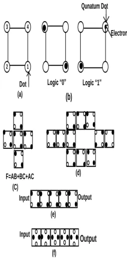
Quantum dot Cellular Automata is emerging Technology in Nanotechnology. QCA consists of four quantum dots positioned at four corners of square (20×20 nm2) cell and two mobile electrons are confined within cell. This was proposed couple of decade before by C.S.Lent .In QCA logic states are defined in terms of polarization of electrons rather than the voltage level. When electrons are polarized P=+1.00 then it implies binary „1‟ equivalent and when electrons are polarized P=-1.00 then it implies binary „0‟ shown Fig 1.a, 1.b.
Launder reported four phase clocking scheme. The four phases are relaxed, switch, hold and release.In the relax phase there is no inter-dot barrier. In the switch phase, barrier is slowly become high and cell attends definite polarity depending on the input. Electrons are polarized due to columbic effects. The polarity retains in the hold phase. The barrier is slowly getting lowered and cell release the polarity in the release phase. The Coulomb interaction between two cells, allows transmitting the information or signalling in QCA cell array. The electrons are only tunnels from one dot to another dot, i.e. electrons are confined within the dots. Electrons are not flow from one QCA cell to another QCA cell. The interaction can be described by Knik energy Ekink.
3 Logic “0” Logic “1”
(b)
(e) (d) (f) Input Output InputOutput
Qunatum Dot Electron 2 1 4 F=AB+BC+AC (C) Dot (a)Fig 1. QCA cell and basic devices (a) QCA 4 Dots (b) QCA cell is logic “1”,and logic “0” (c)MV (d)inverter (INV) (e) binary wire (f)INV chain
II. RELATED WORK
There are number of existing reversible logic gates such as Fredkin gate, Feynman gate, Peres gate, Toffoli gate. Fredkin gate is used for designing such testable sequential circuit is presented. There by avoiding the usage of scan path access to the internal memory cell. Henceforth, testing time can be reduced. Testable sequential circuit can have normal mode and test mode. In the normal mode, the circuit will have feedback but in the test mode, the circuit is made as suitable by disrupting the feedback. So, the circuit is to be tested by only two test vectors (0‟s and 1‟s).
A. CONSERVATIVE REVERSIBLE
FREDKIN GATE
The Fredkin gate is a popularly used reversible conservative logic gate, first proposed by Fredkin and Toffoli in [3][4]. The Fredkin gate shown in Fig. 1 can be described as a mapping (A, B, C) to (P = A, Q = AB + AC, R = AB+ AC), where A, B, C are the inputs and P, Q, R are the outputs, respectively.
F
A
B
C
P=A
Q=A’B+AC
R=AB+A’C
Fig 2 Fredkin gate
1 TABLE
TRUTH TABLE OF FREDKIN GATE
The Sequential circuits are designed using the Fredkin gate achieves only the limited fault coverage. In order to improve that Toffoli gate is a universal gate, also known as controlled-not gate is used. It has 3 inputs and 3 outputs. The truth table for Fredkin gate is shown below.
B. FEYNMAN GATE
FG A B P=A Q=A XOR BFig 3.Feynman gate
The Reversible 2*2 gate with Quantum Cost of one having mapping input (A, B) to output (P = A, Q = A B)[5]
2. TABLE
TRUTH TABLE OF FEYNMAN GATE
C.
DESIGN OF TESTABL REVERSIBLE SEQENTIAL CIRCUITS
The characteristic equation of the D latch can be written as Q+ = D · E + .E · Q. In the proposed work, enable (E) refers to the clock and is used interchangeably in place of clock. When the enable signal (clock) is 1, the value of the input D is reflected at the output that is Q+ = D. While, when E = 0 the latch maintains its previous state, that is Q+ = Q. The reversible Fredkin gate has two of its outputs working as 2:1 MUxes, thus the characteristic equation of the D latch can be mapped to the Fredkin gate (F).The realization
Input Output A B P Q 0 0 0 0 0 1 0 1 1 0 1 1 1 1 1 0 INPUT OUTPUT A B C P Q R 0 0 0 0 0 0 0 0 1 0 0 1 0 1 0 0 1 0 0 1 1 0 1 1 1 0 0 1 0 0 1 0 1 1 1 0 1 1 0 1 0 1 1 1 1 1 1 1
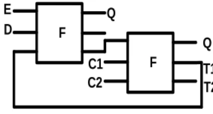
of the reversible D latch using the Fredkin gate. But FO is not allowed in conservative reversible logic[6]. Moreover, the design cannot be tested by two input vectors all 0s and all 1s because of feedback, as the output Q would latch 1 when the inputs are toggled from all 1s to all 0s and could be misinterpreted as stuck-at-1 fault. In this paper, we propose to cascade another Fredkin gate to output Q as shown in Fig. . The design has two control signals, C1 and C2. The design can work in two modes: normal mode and test mode
1. NORMAL MODE
The normal mode is shown in Fig4. in which we will have C1C2 = 01 and we will have the design working as a D latch without any fan-out problem
2. TEST MODE
In test mode, when C1C2 = 00 as shown in Fig. it will make the design testable with all 0s input vectors as output T1 will become 0 resulting in making it testable with all 0s input vectors. Thus, any stuck-at-1 fault can be detected. When C1C2 =11 as shown in Fig 4. the output T1 will
become 1 and the design
will become testable with all 1s
input vectors for any stuck-at-0 fault. It can seen from above that C1 and C2 will disrupt the feedback in test mode, and in normal mode will take care of the fan-out. Thus, our proposed design worksF E D Q F T1 T2 Q C1 C2
Fig 4.Fredkin based D-Latch with control pins as a reversible D latch and can be tested with only two test vectors, all 0s and all 1s, for any stuck-at fault by utilizing the inherent property of conservative reversible logic.
III. PROPOSED REVERSIBLE
D-LATCHES
In this section, we present novel designs of reversible latches that are optimized in terms of area. The D Latch: The characteristic equation of the D latch can be written as Q+ = D· E+ ¯E · Q. When the enable signal(clock) is 1, the value of the input D is reflected at the output that is Q+ = D. F D FG Q E 0 Q
Fig 5(a) Fredkin –Feynman gate based D-latch
While, when E = 0 the latch maintains its previous state, that is Q+ = Q.The characteristic equation of the D latch can be mapped to the Fredkin gate (F) as it matches the template of the Fredkin gate[7]. From the characteristic equation of the D latch Q+ =D.E+E‟Q,we can see that for the four
inputs combinations (E=0,D=0,Q=0),
(E=0,D=1,Q=1),(E=1,D=1,Q=0) and
A.The D Latch with Outputs Q and Q’:
F D FG E 0 Q 1 Q Q’ FGFig 5(b) Fredkin –Feynman gate based D-latch with outputs Q and Q‟
The addition of one garbage output can resolve only two output positions since one bit can
produce only two distinct output
combinations when Q+ is 0.
The design shows in figure 5(a) does not produce the complement output Q‟ which is required often in sequential circuits. We propose a novel design of the D latch that has both the outputs Q and Q‟, and is designed with the 1 Fredkin gate and the2 Feynman gates as shown in Figure 7. In the design, the Feynman gate is used to generate the complement of the output Q.
B. The Negative Enable Reversible D
Latch:
We introduce a design of the reversible D latch that will pass the input D to the output Q when E=0; otherwise maintains the same state. The characteristic equation of such a negative enable D latch can be written as Q+ = D · E¯ + E·Q.
This characteristic equation of the negative enable reversible D latch matches with the template of the Fredkin gate.
F D FG E 0 Q Q
Fig 6(a) Fredkin-Feynman gate based negative enable D latch with only output Q
Thus, it can be mapped on the 2nd output of the Fredkin gate as shown in Figure 6(a). The Feynman gate used in the design plays the role of avoiding the fanout of more than one. In this work, the negative enable D latch is designed with a special purpose of utilizing it in master-slave flip-flops. This is because it will help to design master-slave flip- flops in which no clock inversion is required.The design shown in Figure 6(a) does not have the output Q‟ which can be generated as shown in Figure 6(b).
C. Design of the Reversible
Master-Slave Flip-Flop
The reversible master-slave flip-flops were first presented in Thapliyal et al.[2005] in which the authors had used the strategy of using one latch as a master and the other latch as a slave to design the reversible flip-flops. Figure 7(a) shows the design of the master-slave D flip-flop in which we have used positive enable Fredkin gate based D latch shown in Figure 5(a) as the master latch,[8] while the slave latch is designed from the negative enable Fredkin gate based D latch shown earlier in Figure 6(a).
F
D
FG
E
0
Q
F
FG
Q
0
master
slave
Fig 7 Reversible master-slave D-flip flop It is to be noted that in the proposed master-slave flip-flop designs, the master is designed using the positive enable corresponding latch, while the slave is designed using the negative enable Fredkin gate-based D latch.
Fig 8.QCA layout for Fredkin-Feynman based D- latch with output Q and Q‟.
IV. SIMULATION RESULT:
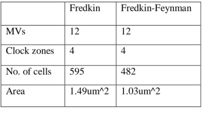
Table 1shows that D-latch designed by Fredkin gate is composed of 595 cells and it covers 1.49 μm2 areas.On the other side D-latch designed by Fredkin-Feynman gate is composed of 482 cells and it covers 1.03 μm2 areas. It is also shown that D-latch designed by
Fredkin-Feynman gate takes a less number of cell and area than the designed by the Fredkin –Fredkin gate.
5.TABLE
COMPARISION TABLE FOR FREDKIN AND FREDKIN -FEYNMAN DLATCH
V. CONCLUSION
This paper presents the design of D-latch using Fredkin-Feynman gate, Fredkin –Feynman gate based d-latch with outputs Q and Q‟, Fredkin-Feynman gate based negative enable D latch with output Q and Q‟and Fredkin – Feynman gate based master-slave D flip-flop.The design is very useful for future computing techniques like ultra low power digital circuits and quantum computers. MVs provide a functionally complete logic set for QCA. It is believed that QCA will become a more practical ways to create a faster and denser circuit. The simulation results show that the proposed circuits perform well. During the design an attention is made to reduce the number of cells as well as to reduce the area. The Fredkin-Feynman gate based D-latch is 28% more efficient than Fredkin based D-latch in terms of area.
Fredkin Fredkin-Feynman
MVs 12 12
Clock zones 4 4
No. of cells 595 482
This paper helps to design, a higher complex computing circuit using reversible gates. Hence, it concludes that the proposed design should be promising step towards the goal of less area design in nanotechnology.
REFERENCES
[1] E. Fredkin and T. Toffoli, “Conservative logic,” Int. J. Theor. Phys., vol. 21, nos. 3–4, pp. 219–253, 1982.
[2]. Himanshu thapiyal, Nagarajan
Ranganathan, ”Design of Testable Reversble sequential Circuits”vol.21, IEEE trans, Jan 2013.
[3].Himanshu thapiyal, Nagarajan
Ranganathan, ”Reversble logic based concurrently testable latches for molecular QCA”vol.9, IEEE trans, Jan 2010.
[4].Mr.Devendra Goyal,and Ms.Vidhi
Sharma,”VHDL Implementation ofReversible Logic Gates” vol.2,may.2012
[5] Md.Anisur Rahman,Fatema Khatun, Angona Sarkar and Md.Fazlul Huq “Design and Implementation of Feynman Gate in Quantum –dot Cellular Automata(QCA). [6] M.K.Nigesh Praveen kumar and A.Arul Rex “Design of Stuck Testable Conservative Logic based Flip-Flops and its Application Circuits”,Vol. 3, No. 2, Mar 2014.
[7] P.Mohan Krishna,V.G.Santhi Swaroopand S.Harika,”Implementation of Optimized ReversibleSequential and Combinational circuits for VLSI Applications”Vol. 4,pp.382-388,April.2014.
[8] H. Thapliyal and N. Ranganathan, “Design of reversible sequential circuits optimizing quantum cost, delay and garbage outputs,” ACM J. Emerg. Technol. Comput. Syst., vol. 6, no. 4, pp. 14:1–14:35, Dec. 2010.