Data Sheet
28/40/44-Pin Enhanced Flash
Microcontrollers
Information contained in this publication regarding device applications and the like is intended through suggestion only and may be superseded by updates. It is your responsibility to ensure that your application meets with your specifications. No representation or warranty is given and no liability is assumed by Microchip Technology Incorporated with respect to the accuracy or use of such information, or infringement of patents or other intellectual property rights arising from such use or otherwise. Use of Microchip’s products as critical components in life support systems is not authorized except with express written approval by Microchip. No licenses are conveyed, implicitly or otherwise, under any intellectual property rights.
Trademarks
The Microchip name and logo, the Microchip logo, Accuron, dsPIC, KEELOQ, MPLAB, PIC, PICmicro, PICSTART, PRO MATE and PowerSmart are registered trademarks of Microchip Technology Incorporated in the U.S.A. and other countries.
AmpLab, FilterLab, microID, MXDEV, MXLAB, PICMASTER, SEEVAL and The Embedded Control Solutions Company are registered trademarks of Microchip Technology Incorporated in the U.S.A.
Application Maestro, dsPICDEM, dsPICDEM.net, ECAN, ECONOMONITOR, FanSense, FlexROM, fuzzyLAB, In-Circuit Serial Programming, ICSP, ICEPIC, microPort, Migratable Memory, MPASM, MPLIB, MPLINK, MPSIM, PICkit, PICDEM, PICDEM.net, PowerCal, PowerInfo, PowerMate, PowerTool, rfLAB, rfPIC, Select Mode, SmartSensor, SmartShunt, SmartTel and Total Endurance are trademarks of Microchip Technology Incorporated in the U.S.A. and other countries.
Serialized Quick Turn Programming (SQTP) is a service mark of Microchip Technology Incorporated in the U.S.A.
All other trademarks mentioned herein are property of their respective companies.
© 2003, Microchip Technology Incorporated, Printed in the U.S.A., All Rights Reserved.
Printed on recycled paper. intended manner and under normal conditions.
• There are dishonest and possibly illegal methods used to breach the code protection feature. All of these methods, to our knowledge, require using the Microchip products in a manner outside the operating specifications contained in Microchip's Data Sheets. Most likely, the person doing so is engaged in theft of intellectual property.
• Microchip is willing to work with the customer who is concerned about the integrity of their code.
• Neither Microchip nor any other semiconductor manufacturer can guarantee the security of their code. Code protection does not mean that we are guaranteeing the product as “unbreakable.”
Code protection is constantly evolving. We at Microchip are committed to continuously improving the code protection features of our products. Attempts to break microchip’s code protection feature may be a violation of the Digital Millennium Copyright Act. If such acts allow unauthorized access to your software or other copyrighted work, you may have a right to sue for relief under that Act.
Microchip received QS-9000 quality system certification for its worldwide headquarters, design and wafer fabrication facilities in Chandler and Tempe, Arizona in July 1999 and Mountain View, California in March 2002. The Company’s quality system processes and
Devices Included in this Data Sheet:
High-Performance RISC CPU:
• Only 35 single-word instructions to learn • All single-cycle instructions except for program
branches, which are two-cycle
• Operating speed: DC – 20 MHz clock input DC – 200 ns instruction cycle • Up to 8K x 14 words of Flash Program Memory,
Up to 368 x 8 bytes of Data Memory (RAM), Up to 256 x 8 bytes of EEPROM Data Memory • Pinout compatible to other 28-pin or 40/44-pin PIC16CXXX and PIC16FXXX microcontrollers
Peripheral Features:
• Timer0: 8-bit timer/counter with 8-bit prescaler • Timer1: 16-bit timer/counter with prescaler,
can be incremented during Sleep via external crystal/clock
• Timer2: 8-bit timer/counter with 8-bit period register, prescaler and postscaler
• Two Capture, Compare, PWM modules - Capture is 16-bit, max. resolution is 12.5 ns - Compare is 16-bit, max. resolution is 200 ns - PWM max. resolution is 10-bit
• Synchronous Serial Port (SSP) with SPI™ (Master mode) and I2C™(Master/Slave) • Universal Synchronous Asynchronous Receiver
Transmitter (USART/SCI) with 9-bit address detection
• Parallel Slave Port (PSP) – 8 bits wide with external RD, WR and CS controls (40/44-pin only) • Brown-out detection circuitry for
Brown-out Reset (BOR)
Analog Features:
• 10-bit, up to 8-channel Analog-to-Digital Converter (A/D)
• Brown-out Reset (BOR)
• Analog Comparator module with: - Two analog comparators
- Programmable on-chip voltage reference (VREF) module
- Programmable input multiplexing from device inputs and internal voltage reference
- Comparator outputs are externally accessible
Special Microcontroller Features:
• 100,000 erase/write cycle Enhanced Flash program memory typical
• 1,000,000 erase/write cycle Data EEPROM memory typical
• Data EEPROM Retention > 40 years • Self-reprogrammable under software control • In-Circuit Serial Programming™ (ICSP™)
via two pins
• Single-supply 5V In-Circuit Serial Programming • Watchdog Timer (WDT) with its own on-chip RC
oscillator for reliable operation • Programmable code protection • Power saving Sleep mode • Selectable oscillator options • In-Circuit Debug (ICD) via two pins
CMOS Technology:
• Low-power, high-speed Flash/EEPROM technology
• Fully static design
• Wide operating voltage range (2.0V to 5.5V) • Commercial and Industrial temperature ranges • Low-power consumption
• PIC16F873A • PIC16F874A
• PIC16F876A • PIC16F877A
Pin Diagrams
PI C 1 6F8 73A /876 A 10 11 2 3 4 5 6 1 8 7 9 12 13 14 15 16 17 18 19 20 23 24 25 26 27 28 22 21 MCLR/VPP RA0/AN0 RA1/AN1 RA2/AN2/VREF-/CVREF RA3/AN3/VREF+ RA4/T0CKI/C1OUT RA5/AN4/SS/C2OUT VSS OSC1/CLKI OSC2/CLKO RC0/T1OSO/T1CKI RC1/T1OSI/CCP2 RC2/CCP1 RC3/SCK/SCL RB7/PGD RB6/PGC RB5 RB4 RB3/PGM RB2 RB1 RB0/INT VDD VSS RC7/RX/DT RC6/TX/CK RC5/SDO RC4/SDI/SDA 28-Pin PDIP, SOIC, SSOP2 3 4 5 6 1 7 MC L R /V PP RA2/AN2/VREF-/CVREF RA3/AN3/VREF+ RA4/T0CKI/C1OUT RA5/AN4/SS/C2OUT VSS OSC1/CLKI 15 16 17 18 19 20 21 RB3/PGM VDD VSS RB0/INT RC7/RX/DT RC1 /T 1 O SI/CCP2 RC2 /CCP1 RC3 /SCK/SCL RC4 /S D I/SDA RC5 /SDO RC 6 /T X /C K 23 24 25 26 27 28 22 RA1 /AN1 RA0 /AN0 RB7 /PGD RB6 /PGC RB5 RB4 10 11 8 9 12 13 14 28-Pin QFN PIC16F873A PIC16F876A RB2 RB1 RC0 /T 1 O SO/ T 1 C K I OSC2/CLKO 10 11 2 3 4 5 6 1
18 19 20 21 22 12 13 14 15
38
8 7
44 43 42 41 40 39
16 17 29 30 31 32 33 23 24 25 26 27 28 36 35 34
9 PIC16F874A 37 N 3 /V RE F + RE F -/C V RE F RA1 /A N 1 RA0 /A N 0 MC L R /V PP RB3 /PGM RB7 /PGD RB6 /PGC RB 5 RB 4 NC RC6 /T X /CK RC5 /SDO RC4 /SDI/SDA RD3 /PSP3 RD2 /PSP2 RD1 /PSP1 RD0 /PSP0 RC3 /SCK/SCL RC2 /CCP1 RC1 /T 1 O SI/ CCP2 RC0/T 1OS O/T 1 C K I OSC2/CLKO OSC1/CLKI VSS VSS VDD VDD RE2/CS/AN7 RE1/WR/AN6 RE0/RD/AN5 RA5/AN4/SS/C2OUT RA4/T0CKI/C1OUT RC7/RX/DT RD4/PSP4 RD5/PSP5 RD6/PSP6 RD7/PSP7 VSS VDD VDD RB0/INT RB1 RB2 44-Pin QFN PIC16F877A
Pin Diagrams (Continued)
RB7/PGD RB6/PGC RB5 RB4 RB3/PGM RB2 RB1 RB0/INT VDD VSS RD7/PSP7 RD6/PSP6 RD5/PSP5 RD4/PSP4 RC7/RX/DT RC6/TX/CK RC5/SDO RC4/SDI/SDA RD3/PSP3 RD2/PSP2 MCLR/VPP RA0/AN0 RA1/AN1 RA2/AN2/VREF-/CVREF RA3/AN3/VREF+ RA4/T0CKI/C1OUT RA5/AN4/SS/C2OUT RE0/RD/AN5 RE1/WR/AN6 RE2/CS/AN7 VDD VSS OSC1/CLKI OSC2/CLKO RC0/T1OSO/T1CKI RC1/T1OSI/CCP2 RC2/CCP1 RC3/SCK/SCL RD0/PSP0 RD1/PSP1 1 2 3 4 5 6 7 8 9 10 11 12 13 14 15 16 17 18 19 20 40 39 38 37 36 35 34 33 32 31 30 29 28 27 26 25 24 23 22 21 PI C 16F8 7 4 A /877 A 40-Pin PDIP 10 11 12 13 14 15 16 1718 19 20 21 22 23 24 25 26
44
8 7
6 5 4 3 2 1
27 28 29 30 31 32 33 34 35 36 37 38 39 40 41 42 43 9 PIC16F874A RA4/T0CKI/C1OUT RA5/AN4/SS/C2OUT RE0/RD/AN5 OSC1/CLKI OSC2/CLKO RC0/T1OSO/T1CK1 NC RE1/WR/AN6 RE2/CS/AN7 VDD VSS RB3/PGM RB2 RB1 RB0/INT VDD VSS RD7/PSP7 RD6/PSP6 RD5/PSP5 RD4/PSP4 RA3 /AN3 /V RE F + R A 2/A N 2/V RE F -/C V RE F RA1 /AN1 RA0 /AN0 MC L R /V PP NC RB7 /PGD RB6 /PGC
RB5 RB4 NC
NC RC6 /T X/CK RC5 /SDO RC4 /SDI/SDA RD3 /PSP3 RD2 /PSP2 RD1 /PSP1 RD0 /PSP0 RC3 /SCK/SCL RC2 /CCP1 R C 1/T 1 OS I/ CCP 2 10 11 2 3 4 5 6 1
18 19 20 21 22 12 13 14 15
38
8 7
44 43 42 41 40 39
16 17 29 30 31 32 33 23 24 25 26 27 28 36 35 34
9 PIC16F874A 37 RC 6 /T X /CK RC 5 /SDO RC 4 /SDI/SDA RD 3 /PSP3 RD 2 /PSP2 RD 1 /PSP1 RD 0 /PSP0 RC 3 /SCK/ SCL RC 2 /CCP1 RC 1 /T 1 OSI/ CCP2 NC NC RC0/T1OSO/T1CKI OSC2/CLKO OSC1/CLKI VSS VDD RE2/CS/AN7 RE1/WR/AN6 RE0/RD/AN5 RA5/AN4/SS/C2OUT RA4/T0CKI/C1OUT RC7/RX/DT RD4/PSP4 RD5/PSP5 RD6/PSP6 RD7/PSP7 VSS VDD RB0/INT RB1 RB2 RB3/PGM 44-Pin PLCC 44-Pin TQFP PIC16F877A PIC16F877A RC7/RX/DT
Table of Contents
1.0 Device Overview ... 5
2.0 Memory Organization... 15
3.0 Data EEPROM and Flash Program Memory ... 33
4.0 I/O Ports... 41
5.0 Timer0 Module ... 53
6.0 Timer1 Module ... 57
7.0 Timer2 Module ... 61
8.0 Capture/Compare/PWM Modules ... 63
9.0 Master Synchronous Serial Port (MSSP) Module... 71
10.0 Addressable Universal Synchronous Asynchronous Receiver Transmitter (USART) ... 111
11.0 Analog-to-Digital Converter (A/D) Module ... 127
12.0 Comparator Module ... 135
13.0 Comparator Voltage Reference Module ... 141
14.0 Special Features of the CPU ... 143
15.0 Instruction Set Summary... 159
16.0 Development Support ... 167
17.0 Electrical Characteristics... 173
18.0 DC and AC Characteristics Graphs and Tables ... 197
19.0 Packaging Information ... 209
Appendix A: Revision History ... 219
Appendix B: Device Differences... 219
Appendix C: Conversion Considerations... 220
Index ... 221
On-Line Support... 229
Systems Information and Upgrade Hot Line ... 229
Reader Response ... 230
PIC16F87XA Product Identification System... 231
TO OUR VALUED CUSTOMERS
It is our intention to provide our valued customers with the best documentation possible to ensure successful use of your Microchip products. To this end, we will continue to improve our publications to better suit your needs. Our publications will be refined and enhanced as new volumes and updates are introduced.
If you have any questions or comments regarding this publication, please contact the Marketing Communications Department via E-mail at [email protected] or fax the Reader Response Form in the back of this data sheet to (480) 792-4150. We welcome your feedback.
Most Current Data Sheet
To obtain the most up-to-date version of this data sheet, please register at our Worldwide Web site at: http://www.microchip.com
You can determine the version of a data sheet by examining its literature number found on the bottom outside corner of any page. The last character of the literature number is the version number, (e.g., DS30000A is version A of document DS30000).
Errata
An errata sheet, describing minor operational differences from the data sheet and recommended workarounds, may exist for current devices. As device/documentation issues become known to us, we will publish an errata sheet. The errata will specify the revision of silicon and revision of document to which it applies.
To determine if an errata sheet exists for a particular device, please check with one of the following:
• Microchip’s Worldwide Web site; http://www.microchip.com • Your local Microchip sales office (see last page)
• The Microchip Corporate Literature Center; U.S. FAX: (480) 792-7277
When contacting a sales office or the literature center, please specify which device, revision of silicon and data sheet (include liter-ature number) you are using.
1.0
DEVICE OVERVIEW
This document contains device specific information about the following devices:
• PIC16F873A • PIC16F874A • PIC16F876A • PIC16F877A
PIC16F873A/876A devices are available only in 28-pin packages, while PIC16F874A/877A devices are avail-able in 40-pin and 44-pin packages. All devices in the PIC16F87XA family share common architecture with the following differences:
• The PIC16F873A and PIC16F874A have one-half of the total on-chip memory of the PIC16F876A and PIC16F877A
• The 28-pin devices have three I/O ports, while the 40/44-pin devices have five
• The 28-pin devices have fourteen interrupts, while the 40/44-pin devices have fifteen
• The 28-pin devices have five A/D input channels, while the 40/44-pin devices have eight
• The Parallel Slave Port is implemented only on the 40/44-pin devices
The available features are summarized in Table 1-1. Block diagrams of the PIC16F873A/876A and PIC16F874A/877A devices are provided in Figure 1-1 and Figure 1-2, respectively. The pinouts for these device families are listed in Table 1-2 and Table 1-3. Additional information may be found in the PICmicro®
Mid-Range Reference Manual (DS33023), which may be obtained from your local Microchip Sales Represen-tative or downloaded from the Microchip web site. The Reference Manual should be considered a complemen-tary document to this data sheet and is highly recom-mended reading for a better understanding of the device architecture and operation of the peripheral modules.
TABLE 1-1: PIC16F87XA DEVICE FEATURES
Key Features PIC16F873A PIC16F874A PIC16F876A PIC16F877A
Operating Frequency DC – 20 MHz DC – 20 MHz DC – 20 MHz DC – 20 MHz Resets (and Delays) POR, BOR
(PWRT, OST)
POR, BOR (PWRT, OST)
POR, BOR (PWRT, OST)
POR, BOR (PWRT, OST) Flash Program Memory
(14-bit words)
4K 4K 8K 8K
Data Memory (bytes) 192 192 368 368 EEPROM Data Memory (bytes) 128 128 256 256 Interrupts 14 15 14 15 I/O Ports Ports A, B, C Ports A, B, C, D, E Ports A, B, C Ports A, B, C, D, E
Timers 3 3 3 3
Capture/Compare/PWM modules 2 2 2 2 Serial Communications MSSP, USART MSSP, USART MSSP, USART MSSP, USART Parallel Communications — PSP — PSP 10-bit Analog-to-Digital Module 5 input channels 8 input channels 5 input channels 8 input channels Analog Comparators 2 2 2 2 Instruction Set 35 Instructions 35 Instructions 35 Instructions 35 Instructions Packages 28-pin PDIP 40-pin PDIP 28-pin PDIP 40-pin PDIP
FIGURE 1-1: PIC16F873A/876A BLOCK DIAGRAM
Flash
13 Data Bus 8
14 Program
Bus
Instruction reg
Program Counter
8 Level Stack (13-bit)
RAM File Registers
Direct Addr 7
RAM Addr(1) 9
Addr MUX Indirect
Addr FSR reg
Status reg
MUX
ALU
W reg Power-up
Timer Oscillator Start-up Timer
Power-on Reset Watchdog
Timer Instruction
Decode & Control
Timing Generation OSC1/CLKI
OSC2/CLKO
MCLR VDD, VSS
PORTA
PORTB
PORTC
RA4/T0CKI/C1OUT RA5/AN4/SS/C2OUT
RB0/INT
RC0/T1OSO/T1CKI RC1/T1OSI/CCP2 RC2/CCP1 RC3/SCK/SCL RC4/SDI/SDA RC5/SDO RC6/TX/CK RC7/RX/DT 8
8
Brown-out Reset
Note 1: Higher order bits are from the Status register.
USART CCP1,2 Synchronous
10-bit A/D
Timer0 Timer1 Timer2
Serial Port
RA3/AN3/VREF+ RA2/AN2/VREF-/CVREF RA1/AN1
RA0/AN0
8
3
Data EEPROM
RB1 RB2 RB3/PGM RB4 RB5 RB6/PGC RB7/PGD
In-Circuit Debugger Low-Voltage Programming
Comparator ReferenceVoltage
Device Program Flash Data Memory Data EEPROM
PIC16F873A 4K words 192 Bytes 128 Bytes
PIC16F876A 8K words 368 Bytes 256 Bytes
Program Memory
FIGURE 1-2: PIC16F874A/877A BLOCK DIAGRAM
13 Data Bus 8
14 Program
Bus
Instruction reg
Program Counter
8 Level Stack (13-bit)
RAM File Registers
Direct Addr 7
RAM Addr(1) 9
Addr MUX Indirect
Addr FSR reg Status reg
MUX
ALU
W reg Power-up
Timer Oscillator Start-up Timer
Power-on Reset Watchdog
Timer Instruction
Decode & Control
Timing Generation OSC1/CLKI
OSC2/CLKO
MCLR VDD, VSS
PORTA
PORTB
PORTC
PORTD
PORTE
RA4/T0CKI/C1OUT RA5/AN4/SS/C2OUT
RC0/T1OSO/T1CKI RC1/T1OSI/CCP2 RC2/CCP1 RC3/SCK/SCL RC4/SDI/SDA RC5/SDO RC6/TX/CK RC7/RX/DT
RE0/RD/AN5 RE1/WR/AN6 RE2/CS/AN7 8
8
Brown-out Reset
RA3/AN3/VREF+ RA2/AN2/VREF-/CVREF RA1/AN1
RA0/AN0
Parallel 8
3
RB0/INT RB1 RB2 RB3/PGM RB4 RB5 RB6/PGC RB7/PGD
In-Circuit Debugger Low-Voltage Programming
RD0/PSP0 RD1/PSP1 RD2/PSP2 RD3/PSP3 RD4/PSP4 RD5/PSP5 RD6/PSP6 RD7/PSP7
USART CCP1,2 Synchronous
10-bit A/D
Timer0 Timer1 Timer2
Serial Port
Data EEPROM Comparator ReferenceVoltage
Device Program Flash Data Memory Data EEPROM
PIC16F874A 4K words 192 Bytes 128 Bytes
Flash Program
Memory
TABLE 1-2: PIC16F873A/876A PINOUT DESCRIPTION
Pin Name PDIP, SOIC, SSOP Pin# QFN Pin# I/O/P Type Buffer Type Description OSC1/CLKI OSC1 CLKI 9 6 I I
ST/CMOS(3) Oscillator crystal or external clock input.
Oscillator crystal input or external clock source input. ST buffer when configured in RC mode; otherwise CMOS. External clock source input. Always associated with pin function OSC1 (see OSC1/CLKI, OSC2/CLKO pins). OSC2/CLKO OSC2 CLKO 10 7 O O
— Oscillator crystal or clock output.
Oscillator crystal output. Connects to crystal or resonator in Crystal Oscillator mode.
In RC mode, OSC2 pin outputs CLKO, which has 1/4 the frequency of OSC1 and denotes the instruction cycle rate. MCLR/VPP MCLR VPP 1 26 I P
ST Master Clear (input) or programming voltage (output). Master Clear (Reset) input. This pin is an active low Reset to the device.
Programming voltage input. PORTA is a bidirectional I/O port. RA0/AN0 RA0 AN0 2 27 I/O I TTL Digital I/O. Analog input 0. RA1/AN1 RA1 AN1 3 28 I/O I TTL Digital I/O. Analog input 1. RA2/AN2/VREF-/ CVREF RA2 AN2 VREF-CVREF 4 1 I/O I I O TTL Digital I/O. Analog input 2.
A/D reference voltage (Low) input. Comparator VREF output. RA3/AN3/VREF+ RA3 AN3 VREF+ 5 2 I/O I I TTL Digital I/O. Analog input 3.
A/D reference voltage (High) input. RA4/T0CKI/C1OUT RA4 T0CKI C1OUT 6 3 I/O I O ST
Digital I/O – Open-drain when configured as output. Timer0 external clock input.
Comparator 1 output. RA5/AN4/SS/C2OUT RA5 AN4 SS C2OUT 7 4 I/O I I O TTL Digital I/O. Analog input 4. SPI slave select input. Comparator 2 output.
Legend: I = input O = output I/O = input/output P = power — = Not used TTL = TTL input ST = Schmitt Trigger input
Note 1: This buffer is a Schmitt Trigger input when configured as the external interrupt.
2: This buffer is a Schmitt Trigger input when used in Serial Programming mode.
PORTB is a bidirectional I/O port. PORTB can be software programmed for internal weak pull-ups on all inputs. RB0/INT RB0 INT 21 18 I/O I TTL/ST(1) Digital I/O. External interrupt.
RB1 22 19 I/O TTL Digital I/O.
RB2 23 20 I/O TTL Digital I/O.
RB3/PGM RB3 PGM 24 21 I/O I TTL Digital I/O.
Low-voltage (single-supply) ICSP programming enable pin.
RB4 25 22 I/O TTL Digital I/O.
RB5 26 23 I/O TTL Digital I/O.
RB6/PGC RB6 PGC 27 24 I/O I TTL/ST(2) Digital I/O.
In-circuit debugger and ICSP programming clock. RB7/PGD RB7 PGD 28 25 I/O I/O TTL/ST(2) Digital I/O.
In-circuit debugger and ICSP programming data. PORTC is a bidirectional I/O port.
RC0/T1OSO/T1CKI RC0 T1OSO T1CKI 11 8 I/O O I ST Digital I/O.
Timer1 oscillator output. Timer1 external clock input. RC1/T1OSI/CCP2 RC1 T1OSI CCP2 12 9 I/O I I/O ST Digital I/O.
Timer1 oscillator input.
Capture2 input, Compare2 output, PWM2 output. RC2/CCP1 RC2 CCP1 13 10 I/O I/O ST Digital I/O.
Capture1 input, Compare1 output, PWM1 output. RC3/SCK/SCL RC3 SCK SCL 14 11 I/O I/O I/O ST Digital I/O.
Synchronous serial clock input/output for SPI mode. Synchronous serial clock input/output for I2C mode. RC4/SDI/SDA RC4 SDI SDA 15 12 I/O I I/O ST Digital I/O. SPI data in. I2C data I/O. RC5/SDO RC5 SDO 16 13 I/O O ST Digital I/O. SPI data out. RC6/TX/CK RC6 TX CK 17 14 I/O O I/O ST Digital I/O.
USART asynchronous transmit. USART1 synchronous clock. RC7/RX/DT RC7 RX 18 15 I/O I ST Digital I/O.
USART asynchronous receive.
TABLE 1-2: PIC16F873A/876A PINOUT DESCRIPTION (CONTINUED)
Pin Name PDIP, SOIC, SSOP Pin# QFN Pin# I/O/P Type Buffer Type Description
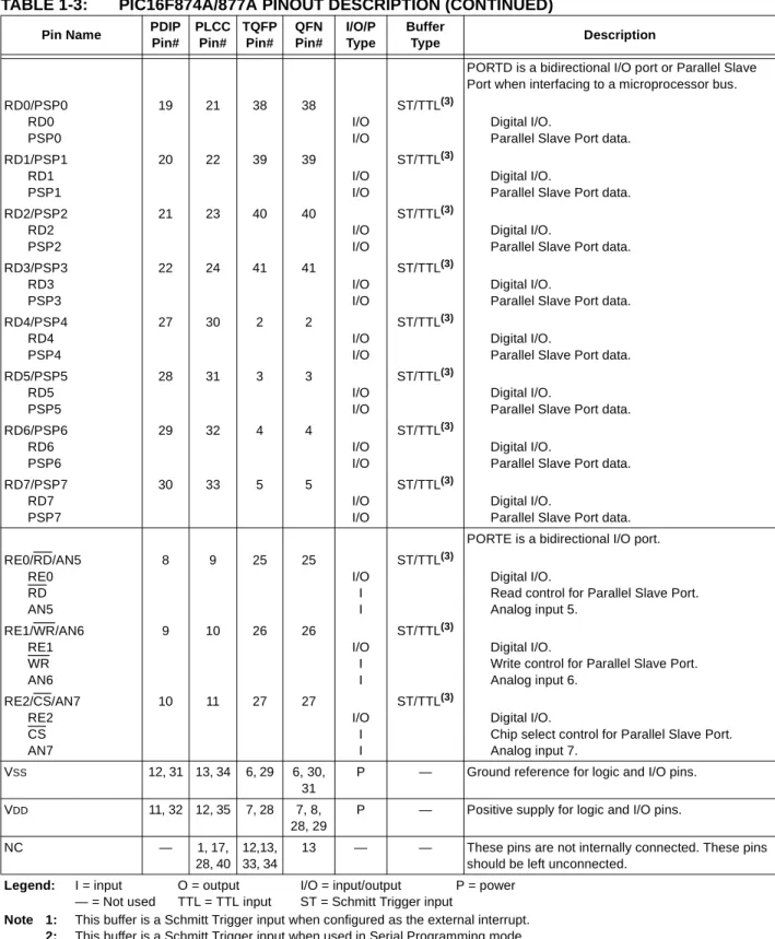
TABLE 1-3: PIC16F874A/877A PINOUT DESCRIPTION
Pin Name PDIP Pin# PLCC Pin# TQFP Pin# QFN Pin# I/O/P Type Buffer Type Description OSC1/CLKI OSC1 CLKI
13 14 30 32
I
I
ST/CMOS(4) Oscillator crystal or external clock input.
Oscillator crystal input or external clock source input. ST buffer when configured in RC mode; otherwise CMOS.
External clock source input. Always associated with pin function OSC1 (see OSC1/CLKI, OSC2/CLKO pins).
OSC2/CLKO OSC2
CLKO
14 15 31 33
O
O
— Oscillator crystal or clock output. Oscillator crystal output.
Connects to crystal or resonator in Crystal Oscillator mode.
In RC mode, OSC2 pin outputs CLKO, which has 1/4 the frequency of OSC1 and denotes the instruction cycle rate.
MCLR/VPP MCLR VPP
1 2 18 18
I P
ST Master Clear (input) or programming voltage (output). Master Clear (Reset) input. This pin is an active low Reset to the device.
Programming voltage input. PORTA is a bidirectional I/O port. RA0/AN0
RA0 AN0
2 3 19 19
I/O I
TTL
Digital I/O. Analog input 0. RA1/AN1
RA1 AN1
3 4 20 20
I/O I
TTL
Digital I/O. Analog input 1. RA2/AN2/VREF-/CVREF
RA2 AN2 VREF-CVREF
4 5 21 21
I/O I I O TTL Digital I/O. Analog input 2.
A/D reference voltage (Low) input. Comparator VREF output. RA3/AN3/VREF+
RA3 AN3 VREF+
5 6 22 22
I/O I I
TTL
Digital I/O. Analog input 3.
A/D reference voltage (High) input. RA4/T0CKI/C1OUT
RA4 T0CKI C1OUT
6 7 23 23
I/O I O
ST
Digital I/O – Open-drain when configured as output.
Timer0 external clock input. Comparator 1 output. RA5/AN4/SS/C2OUT
RA5 AN4 SS C2OUT
7 8 24 24
I/O I I O TTL Digital I/O. Analog input 4. SPI slave select input. Comparator 2 output.
Legend: I = input O = output I/O = input/output P = power — = Not used TTL = TTL input ST = Schmitt Trigger input
Note 1: This buffer is a Schmitt Trigger input when configured as the external interrupt.
2: This buffer is a Schmitt Trigger input when used in Serial Programming mode.
PORTB is a bidirectional I/O port. PORTB can be software programmed for internal weak pull-up on all inputs.
RB0/INT RB0 INT
33 36 8 9
I/O I
TTL/ST(1)
Digital I/O. External interrupt.
RB1 34 37 9 10 I/O TTL Digital I/O.
RB2 35 38 10 11 I/O TTL Digital I/O.
RB3/PGM RB3 PGM
36 39 11 12
I/O I
TTL
Digital I/O.
Low-voltage ICSP programming enable pin.
RB4 37 41 14 14 I/O TTL Digital I/O.
RB5 38 42 15 15 I/O TTL Digital I/O.
RB6/PGC RB6 PGC
39 43 16 16
I/O I
TTL/ST(2)
Digital I/O.
In-circuit debugger and ICSP programming clock. RB7/PGD
RB7 PGD
40 44 17 17
I/O I/O
TTL/ST(2)
Digital I/O.
In-circuit debugger and ICSP programming data.
TABLE 1-3: PIC16F874A/877A PINOUT DESCRIPTION (CONTINUED)
Pin Name PDIP Pin#
PLCC Pin#
TQFP Pin#
QFN Pin#
I/O/P Type
Buffer
Type Description
Legend: I = input O = output I/O = input/output P = power — = Not used TTL = TTL input ST = Schmitt Trigger input
Note 1: This buffer is a Schmitt Trigger input when configured as the external interrupt.
2: This buffer is a Schmitt Trigger input when used in Serial Programming mode.
PORTC is a bidirectional I/O port. RC0/T1OSO/T1CKI
RC0 T1OSO T1CKI
15 16 32 34
I/O O
I
ST
Digital I/O.
Timer1 oscillator output. Timer1 external clock input. RC1/T1OSI/CCP2
RC1 T1OSI CCP2
16 18 35 35
I/O I I/O
ST
Digital I/O.
Timer1 oscillator input.
Capture2 input, Compare2 output, PWM2 output. RC2/CCP1
RC2 CCP1
17 19 36 36
I/O I/O
ST
Digital I/O.
Capture1 input, Compare1 output, PWM1 output. RC3/SCK/SCL
RC3 SCK SCL
18 20 37 37
I/O I/O I/O
ST
Digital I/O.
Synchronous serial clock input/output for SPI mode.
Synchronous serial clock input/output for I2C mode.
RC4/SDI/SDA RC4 SDI SDA
23 25 42 42
I/O I I/O
ST
Digital I/O. SPI data in. I2C data I/O. RC5/SDO
RC5 SDO
24 26 43 43
I/O O
ST
Digital I/O. SPI data out. RC6/TX/CK
RC6 TX CK
25 27 44 44
I/O O I/O
ST
Digital I/O.
USART asynchronous transmit. USART1 synchronous clock. RC7/RX/DT
RC7 RX DT
26 29 1 1
I/O I I/O
ST
Digital I/O.
USART asynchronous receive. USART synchronous data.
TABLE 1-3: PIC16F874A/877A PINOUT DESCRIPTION (CONTINUED)
Pin Name PDIP Pin# PLCC Pin# TQFP Pin# QFN Pin# I/O/P Type Buffer Type Description
Legend: I = input O = output I/O = input/output P = power — = Not used TTL = TTL input ST = Schmitt Trigger input
Note 1: This buffer is a Schmitt Trigger input when configured as the external interrupt.
2: This buffer is a Schmitt Trigger input when used in Serial Programming mode.
PORTD is a bidirectional I/O port or Parallel Slave Port when interfacing to a microprocessor bus. RD0/PSP0
RD0 PSP0
19 21 38 38
I/O I/O
ST/TTL(3)
Digital I/O.
Parallel Slave Port data. RD1/PSP1
RD1 PSP1
20 22 39 39
I/O I/O
ST/TTL(3)
Digital I/O.
Parallel Slave Port data. RD2/PSP2
RD2 PSP2
21 23 40 40
I/O I/O
ST/TTL(3)
Digital I/O.
Parallel Slave Port data. RD3/PSP3
RD3 PSP3
22 24 41 41
I/O I/O
ST/TTL(3)
Digital I/O.
Parallel Slave Port data. RD4/PSP4
RD4 PSP4
27 30 2 2
I/O I/O
ST/TTL(3)
Digital I/O.
Parallel Slave Port data. RD5/PSP5
RD5 PSP5
28 31 3 3
I/O I/O
ST/TTL(3)
Digital I/O.
Parallel Slave Port data. RD6/PSP6
RD6 PSP6
29 32 4 4
I/O I/O
ST/TTL(3)
Digital I/O.
Parallel Slave Port data. RD7/PSP7
RD7 PSP7
30 33 5 5
I/O I/O
ST/TTL(3)
Digital I/O.
Parallel Slave Port data. PORTE is a bidirectional I/O port. RE0/RD/AN5
RE0 RD AN5
8 9 25 25
I/O I I
ST/TTL(3)
Digital I/O.
Read control for Parallel Slave Port. Analog input 5.
RE1/WR/AN6 RE1 WR AN6
9 10 26 26
I/O I I
ST/TTL(3)
Digital I/O.
Write control for Parallel Slave Port. Analog input 6.
RE2/CS/AN7 RE2 CS AN7
10 11 27 27
I/O I I
ST/TTL(3)
Digital I/O.
Chip select control for Parallel Slave Port. Analog input 7.
VSS 12, 31 13, 34 6, 29 6, 30,
31
P — Ground reference for logic and I/O pins.
VDD 11, 32 12, 35 7, 28 7, 8,
28, 29
P — Positive supply for logic and I/O pins.
NC — 1, 17,
28, 40 12,13, 33, 34
13 — — These pins are not internally connected. These pins should be left unconnected.
TABLE 1-3: PIC16F874A/877A PINOUT DESCRIPTION (CONTINUED)
Pin Name PDIP Pin# PLCC Pin# TQFP Pin# QFN Pin# I/O/P Type Buffer Type Description
Legend: I = input O = output I/O = input/output P = power — = Not used TTL = TTL input ST = Schmitt Trigger input
2.0
MEMORY ORGANIZATION
There are three memory blocks in each of the PIC16F87XA devices. The program memory and data memory have separate buses so that concurrent access can occur and is detailed in this section. The EEPROM data memory block is detailed in Section 3.0
“Data EEPROM and Flash Program Memory”.
Additional information on device memory may be found in the PICmicro® Mid-Range MCU Family Reference
Manual (DS33023).
FIGURE 2-1: PIC16F876A/877A
PROGRAM MEMORY MAP AND STACK
2.1
Program Memory Organization
The PIC16F87XA devices have a 13-bit program counter capable of addressing an 8K word x 14 bit program memory space. The PIC16F876A/877A devices have 8K words x 14 bits of Flash program memory, while PIC16F873A/874A devices have 4K words x 14 bits. Accessing a location above the physically implemented address will cause a wraparound.
The Reset vector is at 0000h and the interrupt vector is at 0004h.
FIGURE 2-2: PIC16F873A/874A
PROGRAM MEMORY MAP AND STACK
PC<12:0> 13
0000h
0004h 0005h Stack Level 1
Stack Level 8
Reset Vector
Interrupt Vector
On-Chip
CALL, RETURN RETFIE, RETLW
1FFFh Stack Level 2
Program Memory
Page 0
Page 1
Page 2
Page 3
07FFh 0800h 0FFFh 1000h
17FFh 1800h
PC<12:0> 13
0000h
0004h 0005h Stack Level 1
Stack Level 8
Reset Vector
Interrupt Vector
On-Chip
CALL, RETURN RETFIE, RETLW
1FFFh Stack Level 2
Program Memory
Page 0
Page 1
07FFh 0800h 0FFFh 1000h
2.2
Data Memory Organization
The data memory is partitioned into multiple banks which contain the General Purpose Registers and the Special Function Registers. Bits RP1 (Status<6>) and RP0 (Status<5>) are the bank select bits.
Each bank extends up to 7Fh (128 bytes). The lower locations of each bank are reserved for the Special Function Registers. Above the Special Function Regis-ters are General Purpose RegisRegis-ters, implemented as static RAM. All implemented banks contain Special Function Registers. Some frequently used Special Function Registers from one bank may be mirrored in another bank for code reduction and quicker access.
2.2.1 GENERAL PURPOSE REGISTER FILE
The register file can be accessed either directly, or indirectly, through the File Select Register (FSR).
RP1:RP0 Bank
00 0
01 1
10 2
11 3
Note: The EEPROM data memory description can be found in Section 3.0 “Data EEPROM
and Flash Program Memory” of this data
FIGURE 2-3: PIC16F876A/877A REGISTER FILE MAP
Indirect addr.(*) TMR0 PCL STATUS FSR PORTA PORTB PORTC PCLATH INTCON PIR1 TMR1L TMR1H T1CON TMR2 T2CON SSPBUF SSPCON CCPR1L CCPR1H CCP1CON OPTION_REG PCL STATUS FSR TRISA TRISB TRISC PCLATH INTCON PIE1 PCON PR2 SSPADD SSPSTAT 00h 01h 02h 03h 04h 05h 06h 07h 08h 09h 0Ah 0Bh 0Ch 0Dh 0Eh 0Fh 10h 11h 12h 13h 14h 15h 16h 17h 18h 19h 1Ah 1Bh 1Ch 1Dh 1Eh 1Fh 80h 81h 82h 83h 84h 85h 86h 87h 88h 89h 8Ah 8Bh 8Ch 8Dh 8Eh 8Fh 90h 91h 92h 93h 94h 95h 96h 97h 98h 99h 9Ah 9Bh 9Ch 9Dh 9Eh 9Fh 20h A0h 7Fh FFh File Address
Indirect addr.(*) Indirect addr.(*) PCL STATUS FSR PCLATH INTCON PCL STATUS FSR PCLATH INTCON 100h 101h 102h 103h 104h 105h 106h 107h 108h 109h 10Ah 10Bh 10Ch 10Dh 10Eh 10Fh 110h 111h 112h 113h 114h 115h 116h 117h 118h 119h 11Ah 11Bh 11Ch 11Dh 11Eh 11Fh 180h 181h 182h 183h 184h 185h 186h 187h 188h 189h 18Ah 18Bh 18Ch 18Dh 18Eh 18Fh 190h 191h 192h 193h 194h 195h 196h 197h 198h 199h 19Ah 19Bh 19Ch 19Dh 19Eh 19Fh 120h 1A0h 17Fh 1FFh Indirect addr.(*)
PORTD(1) PORTE(1) TRISD(1) ADRESL TRISE(1) TMR0 OPTION_REG PIR2 PIE2 RCSTA TXREG RCREG CCPR2L CCPR2H CCP2CON ADRESH ADCON0 TXSTA SPBRG ADCON1 General Purpose Register General Purpose Register General Purpose Register General Purpose Register 1EFh 1F0h accesses
70h - 7Fh EFh F0h accesses 70h-7Fh 16Fh 170h accesses 70h-7Fh General Purpose Register General Purpose Register TRISB PORTB 96 Bytes
80 Bytes 80 Bytes 80 Bytes 16 Bytes 16 Bytes SSPCON2 EEDATA EEADR EECON1 EECON2 EEDATH EEADRH Reserved(2) Reserved(2) File Address File Address File Address CMCON CVRCON
FIGURE 2-4: PIC16F873A/874A REGISTER FILE MAP
Indirect addr.(*) TMR0 PCL STATUS FSR PORTA PORTB PORTC PCLATH INTCON PIR1 TMR1L TMR1H T1CON TMR2 T2CON SSPBUF SSPCON CCPR1L CCPR1H CCP1CON OPTION_REG PCL STATUS FSR TRISA TRISB TRISC PCLATH INTCON PIE1 PCON PR2 SSPADD SSPSTAT 00h 01h 02h 03h 04h 05h 06h 07h 08h 09h 0Ah 0Bh 0Ch 0Dh 0Eh 0Fh 10h 11h 12h 13h 14h 15h 16h 17h 18h 19h 1Ah 1Bh 1Ch 1Dh 1Eh 1Fh 80h 81h 82h 83h 84h 85h 86h 87h 88h 89h 8Ah 8Bh 8Ch 8Dh 8Eh 8Fh 90h 91h 92h 93h 94h 95h 96h 97h 98h 99h 9Ah 9Bh 9Ch 9Dh 9Eh 9Fh 20h A0h 7Fh FFh Bank 0 Bank 1
Indirect addr.(*) Indirect addr.(*) PCL STATUS FSR PCLATH INTCON PCL STATUS FSR PCLATH INTCON 100h 101h 102h 103h 104h 105h 106h 107h 108h 109h 10Ah 10Bh 180h 181h 182h 183h 184h 185h 186h 187h 188h 189h 18Ah 18Bh 17Fh 1FFh Bank 2 Bank 3
Indirect addr.(*)
PORTD(1) PORTE(1) TRISD(1) ADRESL TRISE(1) TMR0 OPTION_REG PIR2 PIE2 RCSTA TXREG RCREG CCPR2L CCPR2H CCP2CON ADRESH ADCON0 TXSTA SPBRG ADCON1 General Purpose Register General Purpose Register 1EFh 1F0h accesses
A0h - FFh 16Fh 170h accesses 20h-7Fh TRISB PORTB
96 Bytes 96 Bytes SSPCON2 10Ch 10Dh 10Eh 10Fh 110h 18Ch 18Dh 18Eh 18Fh 190h EEDATA EEADR EECON1 EECON2 EEDATH EEADRH Reserved(2) Reserved(2)
Unimplemented data memory locations, read as ‘0’. * Not a physical register.
120h 1A0h File Address File Address File Address File Address CMCON CVRCON
2.2.2 SPECIAL FUNCTION REGISTERS
The Special Function Registers are registers used by the CPU and peripheral modules for controlling the desired operation of the device. These registers are implemented as static RAM. A list of these registers is given in Table 2-1.
The Special Function Registers can be classified into two sets: core (CPU) and peripheral. Those registers associated with the core functions are described in detail in this section. Those related to the operation of the peripheral features are described in detail in the peripheral features section.
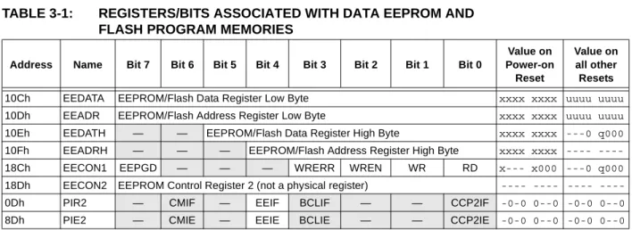
TABLE 2-1: SPECIAL FUNCTION REGISTER SUMMARY
Address Name Bit 7 Bit 6 Bit 5 Bit 4 Bit 3 Bit 2 Bit 1 Bit 0 Value on: POR, BOR
Details on page:
Bank 0
00h(3) INDF Addressing this location uses contents of FSR to address data memory (not a physical register)0000 0000 31, 150
01h TMR0 Timer0 Module Register xxxx xxxx 55, 150
02h(3) PCL Program Counter (PC) Least Significant Byte 0000 0000 30, 150
03h(3) STATUS IRP RP1 RP0 TO PD Z DC C 0001 1xxx 22, 150
04h(3) FSR Indirect Data Memory Address Pointer xxxx xxxx 31, 150
05h PORTA — — PORTA Data Latch when written: PORTA pins when read --0x 0000 43, 150 06h PORTB PORTB Data Latch when written: PORTB pins when read xxxx xxxx 45, 150 07h PORTC PORTC Data Latch when written: PORTC pins when read xxxx xxxx 47, 150 08h(4) PORTD PORTD Data Latch when written: PORTD pins when read xxxx xxxx 48, 150
09h(4) PORTE — — — — — RE2 RE1 RE0 ---- -xxx 49, 150
0Ah(1,3) PCLATH — — — Write Buffer for the upper 5 bits of the Program Counter ---0 0000 30, 150
0Bh(3) INTCON GIE PEIE TMR0IE INTE RBIE TMR0IF INTF RBIF 0000 000x 24, 150
0Ch PIR1 PSPIF(3) ADIF RCIF TXIF SSPIF CCP1IF TMR2IF TMR1IF 0000 0000 26, 150
0Dh PIR2 — CMIF — EEIF BCLIF — — CCP2IF -0-0 0--0 28, 150
0Eh TMR1L Holding Register for the Least Significant Byte of the 16-bit TMR1 Register xxxx xxxx 60, 150 0Fh TMR1H Holding Register for the Most Significant Byte of the 16-bit TMR1 Register xxxx xxxx 60, 150
10h T1CON — — T1CKPS1 T1CKPS0 T1OSCEN T1SYNC TMR1CS TMR1ON --00 0000 57, 150
11h TMR2 Timer2 Module Register 0000 0000 62, 150
12h T2CON — TOUTPS3 TOUTPS2 TOUTPS1 TOUTPS0 TMR2ON T2CKPS1 T2CKPS0 -000 0000 61, 150 13h SSPBUF Synchronous Serial Port Receive Buffer/Transmit Register xxxx xxxx 79, 150
14h SSPCON WCOL SSPOV SSPEN CKP SSPM3 SSPM2 SSPM1 SSPM0 0000 0000 82, 82,
150
15h CCPR1L Capture/Compare/PWM Register 1 (LSB) xxxx xxxx 63, 150
16h CCPR1H Capture/Compare/PWM Register 1 (MSB) xxxx xxxx 63, 150
17h CCP1CON — — CCP1X CCP1Y CCP1M3 CCP1M2 CCP1M1 CCP1M0 --00 0000 64, 150
18h RCSTA SPEN RX9 SREN CREN ADDEN FERR OERR RX9D 0000 000x 112, 150
19h TXREG USART Transmit Data Register 0000 0000 118, 150
1Ah RCREG USART Receive Data Register 0000 0000 118, 150
1Bh CCPR2L Capture/Compare/PWM Register 2 (LSB) xxxx xxxx 63, 150
1Ch CCPR2H Capture/Compare/PWM Register 2 (MSB) xxxx xxxx 63, 150
1Dh CCP2CON — — CCP2X CCP2Y CCP2M3 CCP2M2 CCP2M1 CCP2M0 --00 0000 64, 150
1Eh ADRESH A/D Result Register High Byte xxxx xxxx 133, 150
1Fh ADCON0 ADCS1 ADCS0 CHS2 CHS1 CHS0 GO/DONE — ADON 0000 00-0 127, 150
Legend: x = unknown, u = unchanged, q = value depends on condition, - = unimplemented, read as ‘0’, r = reserved. Shaded locations are unimplemented, read as ‘0’.
Bank 1
80h(3) INDF Addressing this location uses contents of FSR to address data memory (not a physical register)0000 0000 31, 150
81h OPTION_REG RBPU INTEDG T0CS T0SE PSA PS2 PS1 PS0 1111 1111 23, 150
82h(3) PCL Program Counter (PC) Least Significant Byte 0000 0000 30, 150
83h(3) STATUS IRP RP1 RP0 TO PD Z DC C 0001 1xxx 22, 150
84h(3) FSR Indirect Data Memory Address Pointer xxxx xxxx 31, 150
85h TRISA — — PORTA Data Direction Register --11 1111 43, 150
86h TRISB PORTB Data Direction Register 1111 1111 45, 150
87h TRISC PORTC Data Direction Register 1111 1111 47, 150
88h(4) TRISD PORTD Data Direction Register 1111 1111 48, 151
89h(4) TRISE IBF OBF IBOV PSPMODE — PORTE Data Direction bits 0000 -111 50, 151 8Ah(1,3) PCLATH — — — Write Buffer for the upper 5 bits of the Program Counter ---0 0000 30, 150
8Bh(3) INTCON GIE PEIE TMR0IE INTE RBIE TMR0IF INTF RBIF 0000 000x 24, 150
8Ch PIE1 PSPIE(2) ADIE RCIE TXIE SSPIE CCP1IE TMR2IE TMR1IE 0000 0000 25, 151
8Dh PIE2 — CMIE — EEIE BCLIE — — CCP2IE -0-0 0--0 27, 151
8Eh PCON — — — — — — POR BOR ---- --qq 29, 151
8Fh — Unimplemented — —
90h — Unimplemented — —
91h SSPCON2 GCEN ACKSTAT ACKDT ACKEN RCEN PEN RSEN SEN 0000 0000 83, 151
92h PR2 Timer2 Period Register 1111 1111 62, 151
93h SSPADD Synchronous Serial Port (I2C mode) Address Register 0000 0000 79, 151
94h SSPSTAT SMP CKE D/A P S R/W UA BF 0000 0000 79, 151
95h — Unimplemented — —
96h — Unimplemented — —
97h — Unimplemented — —
98h TXSTA CSRC TX9 TXEN SYNC — BRGH TRMT TX9D 0000 -010 111, 151
99h SPBRG Baud Rate Generator Register 0000 0000 113, 151
9Ah — Unimplemented — —
9Bh — Unimplemented — —
9Ch CMCON C2OUT C1OUT C2INV C1INV CIS CM2 CM1 CM0 0000 0111 135, 151
9Dh CVRCON CVREN CVROE CVRR — CVR3 CVR2 CVR1 CVR0 000- 0000 141, 151
9Eh ADRESL A/D Result Register Low Byte xxxx xxxx 133, 151
9Fh ADCON1 ADFM ADCS2 — — PCFG3 PCFG2 PCFG1 PCFG0 00-- 0000 128, 151
TABLE 2-1: SPECIAL FUNCTION REGISTER SUMMARY (CONTINUED)
Address Name Bit 7 Bit 6 Bit 5 Bit 4 Bit 3 Bit 2 Bit 1 Bit 0 Value on: POR, BOR
Details on page:
Legend: x = unknown, u = unchanged, q = value depends on condition, - = unimplemented, read as ‘0’, r = reserved. Shaded locations are unimplemented, read as ‘0’.
Note 1: The upper byte of the program counter is not directly accessible. PCLATH is a holding register for the PC<12:8>, whose contents are transferred to the upper byte of the program counter.
2: Bits PSPIE and PSPIF are reserved on PIC16F873A/876A devices; always maintain these bits clear.
3: These registers can be addressed from any bank.
4: PORTD, PORTE, TRISD and TRISE are not implemented on PIC16F873A/876A devices, read as ‘0’.
Bank 2
100h(3) INDF Addressing this location uses contents of FSR to address data memory (not a physical register)0000 0000 31, 150
101h TMR0 Timer0 Module Register xxxx xxxx 55, 150
102h(3) PCL Program Counter’s (PC) Least Significant Byte 0000 0000 30, 150
103h(3) STATUS IRP RP1 RP0 TO PD Z DC C 0001 1xxx 22, 150
104h(3) FSR Indirect Data Memory Address Pointer xxxx xxxx 31, 150
105h — Unimplemented — —
106h PORTB PORTB Data Latch when written: PORTB pins when read xxxx xxxx 45, 150
107h — Unimplemented — —
108h — Unimplemented — —
109h — Unimplemented — —
10Ah(1,3) PCLATH — — — Write Buffer for the upper 5 bits of the Program Counter ---0 0000 30, 150
10Bh(3) INTCON GIE PEIE TMR0IE INTE RBIE TMR0IF INTF RBIF 0000 000x 24, 150
10Ch EEDATA EEPROM Data Register Low Byte xxxx xxxx 39, 151
10Dh EEADR EEPROM Address Register Low Byte xxxx xxxx 39, 151
10Eh EEDATH — — EEPROM Data Register High Byte --xx xxxx 39, 151
10Fh EEADRH — — — —(5) EEPROM Address Register High Byte ---- xxxx 39, 151
Bank 3
180h(3) INDF Addressing this location uses contents of FSR to address data memory (not a physical register)0000 0000 31, 150
181h OPTION_REG RBPU INTEDG T0CS T0SE PSA PS2 PS1 PS0 1111 1111 23, 150
182h(3) PCL Program Counter (PC) Least Significant Byte 0000 0000 30, 150
183h(3) STATUS IRP RP1 RP0 TO PD Z DC C 0001 1xxx 22, 150
184h(3) FSR Indirect Data Memory Address Pointer xxxx xxxx 31, 150
185h — Unimplemented — —
186h TRISB PORTB Data Direction Register 1111 1111 45, 150
187h — Unimplemented — —
188h — Unimplemented — —
189h — Unimplemented — —
18Ah(1,3) PCLATH — — — Write Buffer for the upper 5 bits of the Program Counter ---0 0000 30, 150
18Bh(3) INTCON GIE PEIE TMR0IE INTE RBIE TMR0IF INTF RBIF 0000 000x 24, 150
18Ch EECON1 EEPGD — — — WRERR WREN WR RD x--- x000 34, 151
18Dh EECON2 EEPROM Control Register 2 (not a physical register) ---- ---- 39, 151
18Eh — Reserved; maintain clear 0000 0000 —
18Fh — Reserved; maintain clear 0000 0000 —
TABLE 2-1: SPECIAL FUNCTION REGISTER SUMMARY (CONTINUED)
Address Name Bit 7 Bit 6 Bit 5 Bit 4 Bit 3 Bit 2 Bit 1 Bit 0 Value on: POR, BOR
Details on page:
Legend: x = unknown, u = unchanged, q = value depends on condition, - = unimplemented, read as ‘0’, r = reserved. Shaded locations are unimplemented, read as ‘0’.
Note 1: The upper byte of the program counter is not directly accessible. PCLATH is a holding register for the PC<12:8>, whose contents are transferred to the upper byte of the program counter.
2: Bits PSPIE and PSPIF are reserved on PIC16F873A/876A devices; always maintain these bits clear.
3: These registers can be addressed from any bank.
4: PORTD, PORTE, TRISD and TRISE are not implemented on PIC16F873A/876A devices, read as ‘0’.
2.2.2.1 Status Register
The Status register contains the arithmetic status of the ALU, the Reset status and the bank select bits for data memory.
The Status register can be the destination for any instruction, as with any other register. If the Status reg-ister is the destination for an instruction that affects the Z, DC or C bits, then the write to these three bits is dis-abled. These bits are set or cleared according to the device logic. Furthermore, the TO and PD bits are not writable, therefore, the result of an instruction with the Status register as destination may be different than intended.
For example, CLRF STATUS, will clear the upper three bits and set the Z bit. This leaves the Status register as
000u u1uu (where u = unchanged).
It is recommended, therefore, that only BCF, BSF,
SWAPF and MOVWF instructions are used to alter the Status register because these instructions do not affect the Z, C or DC bits from the Status register. For other instructions not affecting any status bits, see
Section 15.0 “Instruction Set Summary”.
REGISTER 2-1: STATUS REGISTER (ADDRESS 03h, 83h, 103h, 183h)
Note: The C and DC bits operate as a borrow and digit borrow bit, respectively, in sub-traction. See the SUBLW and SUBWF
instructions for examples.
R/W-0 R/W-0 R/W-0 R-1 R-1 R/W-x R/W-x R/W-x IRP RP1 RP0 TO PD Z DC C
bit 7 bit 0
bit 7 IRP: Register Bank Select bit (used for indirect addressing) 1 = Bank 2, 3 (100h-1FFh)
0 = Bank 0, 1 (00h-FFh)
bit 6-5 RP1:RP0: Register Bank Select bits (used for direct addressing) 11 = Bank 3 (180h-1FFh)
10 = Bank 2 (100h-17Fh)
01 = Bank 1 (80h-FFh)
00 = Bank 0 (00h-7Fh) Each bank is 128 bytes. bit 4 TO: Time-out bit
1 = After power-up, CLRWDT instruction or SLEEP instruction
0 = A WDT time-out occurred bit 3 PD: Power-down bit
1 = After power-up or by the CLRWDT instruction
0 = By execution of the SLEEP instruction bit 2 Z: Zero bit
1 = The result of an arithmetic or logic operation is zero
0 = The result of an arithmetic or logic operation is not zero
bit 1 DC: Digit carry/borrow bit (ADDWF, ADDLW,SUBLW,SUBWF instructions) (for borrow, the polarity is reversed)
1 = A carry-out from the 4th low order bit of the result occurred
0 = No carry-out from the 4th low order bit of the result
bit 0 C: Carry/borrow bit (ADDWF, ADDLW,SUBLW,SUBWF instructions)
1 = A carry-out from the Most Significant bit of the result occurred
0 = No carry-out from the Most Significant bit of the result occurred
Note: For borrow, the polarity is reversed. A subtraction is executed by adding the two’s complement of the second operand. For rotate (RRF, RLF) instructions, this bit is loaded with either the high, or low order bit of the source register.
2.2.2.2 OPTION_REG Register
The OPTION_REG Register is a readable and writable register, which contains various control bits to configure the TMR0 prescaler/WDT postscaler (single assign-able register known also as the prescaler), the external INT interrupt, TMR0 and the weak pull-ups on PORTB.
REGISTER 2-2: OPTION_REG REGISTER (ADDRESS 81h, 181h)
Note: To achieve a 1:1 prescaler assignment for the TMR0 register, assign the prescaler to the Watchdog Timer.
R/W-1 R/W-1 R/W-1 R/W-1 R/W-1 R/W-1 R/W-1 R/W-1 RBPU INTEDG T0CS T0SE PSA PS2 PS1 PS0
bit 7 bit 0
bit 7 RBPU: PORTB Pull-up Enable bit 1 = PORTB pull-ups are disabled
0 = PORTB pull-ups are enabled by individual port latch values bit 6 INTEDG: Interrupt Edge Select bit
1 = Interrupt on rising edge of RB0/INT pin
0 = Interrupt on falling edge of RB0/INT pin bit 5 T0CS: TMR0 Clock Source Select bit
1 = Transition on RA4/T0CKI pin
0 = Internal instruction cycle clock (CLKO) bit 4 T0SE: TMR0 Source Edge Select bit
1 = Increment on high-to-low transition on RA4/T0CKI pin
0 = Increment on low-to-high transition on RA4/T0CKI pin bit 3 PSA: Prescaler Assignment bit
1 = Prescaler is assigned to the WDT
0 = Prescaler is assigned to the Timer0 module bit 2-0 PS2:PS0: Prescaler Rate Select bits
Legend:
R = Readable bit W = Writable bit U = Unimplemented bit, read as ‘0’ - n = Value at POR ‘1’ = Bit is set ‘0’ = Bit is cleared x = Bit is unknown
Note: When using Low-Voltage ICSP Programming (LVP) and the pull-ups on PORTB are enabled, bit 3 in the TRISB register must be cleared to disable the pull-up on RB3
000 001 010 011 100 101 110 111
1 : 2 1 : 4 1 : 8 1 : 16 1 : 32 1 : 64 1 : 128 1 : 256
1 : 1 1 : 2 1 : 4 1 : 8 1 : 16 1 : 32 1 : 64 1 : 128 Bit Value TMR0 Rate WDT Rate
2.2.2.3 INTCON Register
The INTCON register is a readable and writable regis-ter, which contains various enable and flag bits for the TMR0 register overflow, RB port change and external RB0/INT pin interrupts.
REGISTER 2-3: INTCON REGISTER (ADDRESS 0Bh, 8Bh, 10Bh, 18Bh)
Note: Interrupt flag bits are set when an interrupt condition occurs regardless of the state of its corresponding enable bit or the global enable bit, GIE (INTCON<7>). User software should ensure the appropriate interrupt flag bits are clear prior to enabling an interrupt.
R/W-0 R/W-0 R/W-0 R/W-0 R/W-0 R/W-0 R/W-0 R/W-x GIE PEIE TMR0IE INTE RBIE TMR0IF INTF RBIF
bit 7 bit 0
bit 7 GIE: Global Interrupt Enable bit 1 = Enables all unmasked interrupts
0 = Disables all interrupts
bit 6 PEIE: Peripheral Interrupt Enable bit
1 = Enables all unmasked peripheral interrupts
0 = Disables all peripheral interrupts
bit 5 TMR0IE: TMR0 Overflow Interrupt Enable bit 1 = Enables the TMR0 interrupt
0 = Disables the TMR0 interrupt
bit 4 INTE: RB0/INT External Interrupt Enable bit 1 = Enables the RB0/INT external interrupt
0 = Disables the RB0/INT external interrupt bit 3 RBIE: RB Port Change Interrupt Enable bit
1 = Enables the RB port change interrupt
0 = Disables the RB port change interrupt bit 2 TMR0IF: TMR0 Overflow Interrupt Flag bit
1 = TMR0 register has overflowed (must be cleared in software)
0 = TMR0 register did not overflow bit 1 INTF: RB0/INT External Interrupt Flag bit
1 = The RB0/INT external interrupt occurred (must be cleared in software)
0 = The RB0/INT external interrupt did not occur bit 0 RBIF: RB Port Change Interrupt Flag bit
1 = At least one of the RB7:RB4 pins changed state; a mismatch condition will continue to set the bit. Reading PORTB will end the mismatch condition and allow the bit to be cleared (must be cleared in software).
0 = None of the RB7:RB4 pins have changed state
Legend:
R = Readable bit W = Writable bit U = Unimplemented bit, read as ‘0’ - n = Value at POR ‘1’ = Bit is set ‘0’ = Bit is cleared x = Bit is unknown
2.2.2.4 PIE1 Register
The PIE1 register contains the individual enable bits for the peripheral interrupts.
REGISTER 2-4: PIE1 REGISTER (ADDRESS 8Ch)
Note: Bit PEIE (INTCON<6>) must be set to enable any peripheral interrupt.
R/W-0 R/W-0 R/W-0 R/W-0 R/W-0 R/W-0 R/W-0 R/W-0 PSPIE(1) ADIE RCIE TXIE SSPIE CCP1IE TMR2IE TMR1IE
bit 7 bit 0
bit 7 PSPIE: Parallel Slave Port Read/Write Interrupt Enable bit(1) 1 = Enables the PSP read/write interrupt
0 = Disables the PSP read/write interrupt
Note 1: PSPIE is reserved on PIC16F873A/876A devices; always maintain this bit clear.
bit 6 ADIE: A/D Converter Interrupt Enable bit 1 = Enables the A/D converter interrupt
0 = Disables the A/D converter interrupt bit 5 RCIE: USART Receive Interrupt Enable bit
1 = Enables the USART receive interrupt
0 = Disables the USART receive interrupt bit 4 TXIE: USART Transmit Interrupt Enable bit
1 = Enables the USART transmit interrupt
0 = Disables the USART transmit interrupt
bit 3 SSPIE: Synchronous Serial Port Interrupt Enable bit 1 = Enables the SSP interrupt
0 = Disables the SSP interrupt bit 2 CCP1IE: CCP1 Interrupt Enable bit
1 = Enables the CCP1 interrupt
0 = Disables the CCP1 interrupt
bit 1 TMR2IE: TMR2 to PR2 Match Interrupt Enable bit 1 = Enables the TMR2 to PR2 match interrupt
0 = Disables the TMR2 to PR2 match interrupt bit 0 TMR1IE: TMR1 Overflow Interrupt Enable bit
1 = Enables the TMR1 overflow interrupt
0 = Disables the TMR1 overflow interrupt
Legend:
R = Readable bit W = Writable bit U = Unimplemented bit, read as ‘0’ - n = Value at POR ‘1’ = Bit is set ‘0’ = Bit is cleared x = Bit is unknown
2.2.2.5 PIR1 Register
The PIR1 register contains the individual flag bits for the peripheral interrupts.
REGISTER 2-5: PIR1 REGISTER (ADDRESS 0Ch)
Note: Interrupt flag bits are set when an interrupt condition occurs regardless of the state of its corresponding enable bit or the global enable bit, GIE (INTCON<7>). User software should ensure the appropriate interrupt bits are clear prior to enabling an interrupt.
R/W-0 R/W-0 R-0 R-0 R/W-0 R/W-0 R/W-0 R/W-0 PSPIF(1) ADIF RCIF TXIF SSPIF CCP1IF TMR2IF TMR1IF
bit 7 bit 0
bit 7 PSPIF: Parallel Slave Port Read/Write Interrupt Flag bit(1)
1 = A read or a write operation has taken place (must be cleared in software)
0 = No read or write has occurred
Note 1: PSPIF is reserved on PIC16F873A/876A devices; always maintain this bit clear.
bit 6 ADIF: A/D Converter Interrupt Flag bit 1 = An A/D conversion completed
0 = The A/D conversion is not complete bit 5 RCIF: USART Receive Interrupt Flag bit
1 = The USART receive buffer is full
0 = The USART receive buffer is empty bit 4 TXIF: USART Transmit Interrupt Flag bit
1 = The USART transmit buffer is empty
0 = The USART transmit buffer is full
bit 3 SSPIF: Synchronous Serial Port (SSP) Interrupt Flag bit
1 = The SSP interrupt condition has occurred and must be cleared in software before returning from the Interrupt Service Routine. The conditions that will set this bit are:
• SPI – A transmission/reception has taken place. • I2C Slave – A transmission/reception has taken place. • I2C Master
- A transmission/reception has taken place.
- The initiated Start condition was completed by the SSP module. - The initiated Stop condition was completed by the SSP module. - The initiated Restart condition was completed by the SSP module. - The initiated Acknowledge condition was completed by the SSP module. - A Start condition occurred while the SSP module was Idle (multi-master system). - A Stop condition occurred while the SSP module was Idle (multi-master system).
0 = No SSP interrupt condition has occurred bit 2 CCP1IF: CCP1 Interrupt Flag bit
Capture mode:
1 = A TMR1 register capture occurred (must be cleared in software)
0 = No TMR1 register capture occurred Compare mode:
1 = A TMR1 register compare match occurred (must be cleared in software)
0 = No TMR1 register compare match occurred PWM mode:
Unused in this mode.
bit 1 TMR2IF: TMR2 to PR2 Match Interrupt Flag bit
1 = TMR2 to PR2 match occurred (must be cleared in software)
0 = No TMR2 to PR2 match occurred bit 0 TMR1IF: TMR1 Overflow Interrupt Flag bit
1 = TMR1 register overflowed (must be cleared in software)
2.2.2.6 PIE2 Register
The PIE2 register contains the individual enable bits for the CCP2 peripheral interrupt, the SSP bus collision interrupt, EEPROM write operation interrupt and the comparator interrupt.
REGISTER 2-6: PIE2 REGISTER (ADDRESS 8Dh)
Note: Bit PEIE (INTCON<6>) must be set to enable any peripheral interrupt.
U-0 R/W-0 U-0 R/W-0 R/W-0 U-0 U-0 R/W-0 — CMIE — EEIE BCLIE — — CCP2IE
bit 7 bit 0
bit 7 Unimplemented: Read as ‘0’
bit 6 CMIE: Comparator Interrupt Enable bit 1 = Enables the comparator interrupt
0 = Disable the comparator interrupt bit 5 Unimplemented: Read as ‘0’
bit 4 EEIE: EEPROM Write Operation Interrupt Enable bit 1 = Enable EEPROM write interrupt
0 = Disable EEPROM write interrupt bit 3 BCLIE: Bus Collision Interrupt Enable bit
1 = Enable bus collision interrupt
0 = Disable bus collision interrupt bit 2-1 Unimplemented: Read as ‘0’ bit 0 CCP2IE: CCP2 Interrupt Enable bit
1 = Enables the CCP2 interrupt
0 = Disables the CCP2 interrupt
Legend:
R = Readable bit W = Writable bit U = Unimplemented bit, read as ‘0’ - n = Value at POR ‘1’ = Bit is set ‘0’ = Bit is cleared x = Bit is unknown
2.2.2.7 PIR2 Register
The PIR2 register contains the flag bits for the CCP2 interrupt, the SSP bus collision interrupt, EEPROM write operation interrupt and the comparator interrupt.
REGISTER 2-7: PIR2 REGISTER (ADDRESS 0Dh)
Note: Interrupt flag bits are set when an interrupt condition occurs regardless of the state of its corresponding enable bit or the global enable bit, GIE (INTCON<7>). User software should ensure the appropriate interrupt flag bits are clear prior to enabling an interrupt.
U-0 R/W-0 U-0 R/W-0 R/W-0 U-0 U-0 R/W-0 — CMIF — EEIF BCLIF — — CCP2IF
bit 7 bit 0
bit 7 Unimplemented: Read as ‘0’ bit 6 CMIF: Comparator Interrupt Flag bit
1 = The comparator input has changed (must be cleared in software)
0 = The comparator input has not changed bit 5 Unimplemented: Read as ‘0’
bit 4 EEIF: EEPROM Write Operation Interrupt Flag bit
1 = The write operation completed (must be cleared in software)
0 = The write operation is not complete or has not been started bit 3 BCLIF: Bus Collision Interrupt Flag bit
1 = A bus collision has occurred in the SSP when configured for I2C Master mode
0 = No bus collision has occurred bit 2-1 Unimplemented: Read as ‘0’ bit 0 CCP2IF: CCP2 Interrupt Flag bit
Capture mode:
1 = A TMR1 register capture occurred (must be cleared in software)
0 = No TMR1 register capture occurred Compare mode:
1 = A TMR1 register compare match occurred (must be cleared in software)
0 = No TMR1 register compare match occurred PWM mode:
Unused.
Legend:
R = Readable bit W = Writable bit U = Unimplemented bit, read as ‘0’ - n = Value at POR ‘1’ = Bit is set ‘0’ = Bit is cleared x = Bit is unknown
2.2.2.8 PCON Register
The Power Control (PCON) register contains flag bits to allow differentiation between a Power-on Reset (POR), a Brown-out Reset (BOR), a Watchdog Reset (WDT) and an external MCLR Reset.
REGISTER 2-8: PCON REGISTER (ADDRESS 8Eh)
Note: BOR is unknown on Power-on Reset. It must be set by the user and checked on subsequent Resets to see if BOR is clear, indicating a brown-out has occurred. The BOR status bit is a “don’t care” and is not predictable if the brown-out circuit is dis-abled (by clearing the BODEN bit in the configuration word).
U-0 U-0 U-0 U-0 U-0 U-0 R/W-0 R/W-1 — — — — — — POR BOR
bit 7 bit 0
bit 7-2 Unimplemented: Read as ‘0’ bit 1 POR: Power-on Reset Status bit
1 = No Power-on Reset occurred
0 = A Power-on Reset occurred (must be set in software after a Power-on Reset occurs) bit 0 BOR: Brown-out Reset Status bit
1 = No Brown-out Reset occurred
0 = A Brown-out Reset occurred (must be set in software after a Brown-out Reset occurs)
Legend:
R = Readable bit W = Writable bit U = Unimplemented bit, read as ‘0’ - n = Value at POR ‘1’ = Bit is set ‘0’ = Bit is cleared x = Bit is unknown
2.3
PCL and PCLATH
The Program Counter (PC) is 13 bits wide. The low byte comes from the PCL register which is a readable and writable register. The upper bits (PC<12:8>) are not readable, but are indirectly writable through the PCLATH register. On any Reset, the upper bits of the PC will be cleared. Figure 2-5 shows the two situations for the loading of the PC. The upper example in the figure shows how the PC is loaded on a write to PCL (PCLATH<4:0> → PCH). The lower example in the figure shows how the PC is loaded during a CALL or
GOTO instruction (PCLATH<4:3> → PCH).
FIGURE 2-5: LOADING OF PC IN
DIFFERENT SITUATIONS
2.3.1 COMPUTED GOTO
A computed GOTO is accomplished by adding an offset to the program counter (ADDWF PCL). When doing a table read using a computed GOTO method, care should be exercised if the table location crosses a PCL memory boundary (each 256-byte block). Refer to the application note, AN556, “Implementing a Table Read” (DS00556).
2.3.2 STACK
The PIC16F87XA family has an 8-level deep x 13-bit wide hardware stack. The stack space is not part of either program or data space and the stack pointer is not readable or writable. The PC is PUSHed onto the stack when a CALL instruction is executed, or an interrupt causes a branch. The stack is POP’ed in the event of a
RETURN, RETLW or a RETFIE instruction execution. PCLATH is not affected by a PUSH or POP operation. The stack operates as a circular buffer. This means that after the stack has been PUSHed eight times, the ninth push overwrites the value that was stored from the first
2.4
Program Memory Paging
All PIC16F87XA devices are capable of addressing a continuous 8K word block of program memory. The
CALL and GOTO instructions provide only 11 bits of address to allow branching within any 2K program memory page. When doing a CALL or GOTO instruction, the upper 2 bits of the address are provided by PCLATH<4:3>. When doing a CALL or GOTO instruc-tion, the user must ensure that the page select bits are programmed so that the desired program memory page is addressed. If a return from a CALL instruction (or interrupt) is executed, the entire 13-bit PC is popped off the stack. Therefore, manipulation of the PCLATH<4:3> bits is not required for the RETURN
instructions (which POPs the address from the stack).
Example 2-1 shows the calling of a subroutine in page 1 of the program memory. This example assumes that PCLATH is saved and restored by the Interrupt Service Routine(if interrupts are used).
EXAMPLE 2-1: CALL OF A SUBROUTINE
IN PAGE 1 FROM PAGE 0 PC
12 8 7 0
5 PCLATH<4:0>
PCLATH
Instruction with
ALU
GOTO,CALL
Opcode <10:0> 8
PC
12 11 10 0
11 PCLATH<4:3>
PCH PCL
8 7
2
PCLATH
PCH PCL
PCL as Destination
Note 1: There are no status bits to indicate stack
overflow or stack underflow conditions.
2: There are no instructions/mnemonics
called PUSH or POP. These are actions that occur from the execution of the CALL,
RETURN, RETLW and RETFIE instructions or the vectoring to an interrupt address.
Note: The contents of the PCLATH register are unchanged after a RETURN or RETFIE
instruction is executed. The user must rewrite the contents of the PCLATH regis-ter for any subsequent subroutine calls or
GOTO instructions.
ORG 0x500 BCF PCLATH,4
BSF PCLATH,3 ;Select page 1 ;(800h-FFFh)
CALL SUB1_P1 ;Call subroutine in : ;page 1 (800h-FFFh) :
ORG 0x900 ;page 1 (800h-FFFh) SUB1_P1
: ;called subroutine ;page 1 (800h-FFFh) :
RETURN ;return to ;Call subroutine ;in page 0 ;(000h-7FFh)
2.5
Indirect Addressing, INDF and
FSR Registers
The INDF register is not a physical register. Addressing the INDF register will cause indirect addressing. Indirect addressing is possible by using the INDF reg-ister. Any instruction using the INDF register actually accesses the register pointed to by the File Select Reg-ister, FSR. Reading the INDF register itself, indirectly (FSR = 0) will read 00h. Writing to the INDF register indirectly results in a no operation (although status bits may be affected). An effective 9-bit address is obtained by concatenating the 8-bit FSR register and the IRP bit (Status<7>) as shown in Figure 2-6.
A simple program to clear RAM locations 20h-2Fh using indirect addressing is shown in Example 2-2.
EXAMPLE 2-2: INDIRECT ADDRESSING
FIGURE 2-6: DIRECT/INDIRECT ADDRESSING
MOVLW 0x20 ;initialize pointer MOVWF FSR ;to RAM
NEXT CLRF INDF ;clear INDF register INCF FSR,F ;inc pointer
BTFSS FSR,4 ;all done? GOTO NEXT ;no clear next CONTINUE
: ;yes continue
Note 1: For register file map detail, see Figure 2-3.
Data Memory(1)
Indirect Addressing Direct Addressing
Bank Select Location Select
RP1:RP0 6 From Opcode 0 IRP 7 FSR Register 0
Bank Select Location Select
00 01 10 11
Bank 0 Bank 1 Bank 2 Bank 3 FFh
80h
7Fh 00h
17Fh 100h
1FFh 180h
3.0
DATA EEPROM AND FLASH
PROGRAM MEMORY
The data EEPROM and Flash program memory is read-able and writread-able during normal operation (over the full VDD range). This memory is not directly mapped in the register file space. Instead, it is indirectly addressed through the Special Function Registers. There are six SFRs used to read and write this memory:
• EECON1 • EECON2 • EEDATA • EEDATH • EEADR • EEADRH
When interfacing to the data memory block, EEDATA holds the 8-bit data for read/write and EEADR holds the address of the EEPROM location being accessed. These devices have 128 or 256 bytes of data EEPROM (depending on the device), with an address range from 00h to FFh. On devices with 128 bytes, addresses from 80h to FFh are unimplemented and will wraparound to the beginning of data EEPROM memory. When writing to unimplemented locations, the on-chip charge pump will be turned off.
When interfacing the program memory block, the EEDATA and EEDATH registers form a two-byte word that holds the 14-bit data for read/write and the EEADR and EEADRH registers form a two-byte word that holds the 13-bit address of the program memory location being accessed. These devices have 4 or 8K words of program Flash, with an address range from 0000h to 0FFFh for the PIC16F873A/874A and 0000h to 1FFFh for the PIC16F876A/877A. Addresses above the range of the respective device will wraparound to the beginning of program memory.
The EEPROM data memory allows single-byte read and write. The Flash program memory allows single-word reads and four-word block writes. Program memory write operations automatically perform an erase-before-write on blocks of four words. A byte erase-before-write in data EEPROM memory automatically erases the location and writes the new data (erase-before-write).
The write time is controlled by an on-chip timer. The write/erase voltages are generated by an on-chip charge pump, rated to operate over the voltage range of the device for byte or word operations.
When the device is code-protected, the CPU may
3.1
EEADR and EEADRH
The EEADRH:EEADR register pair can address up to a maximum of 256 bytes of data EEPROM or up to a maximum of 8K words of program EEPROM. When selecting a data address value, only the LSByte of the address is written to the EEADR register. When select-ing a program address value, the MSByte of the address is written to the EEADRH register and the LSByte is written to the EEADR register.
If the device contains less memory than the full address reach of the address register pair, the Most Significant bits of the registers are not implemented. For example, if the device has 128 bytes of data EEPROM, the Most Significant bit of EEADR is not implemented on access to data EEPROM.
3.2
EECON1 and EECON2 Registers
EECON1 is the control register for memory accesses. Control bit, EEPGD, determines if the access will be a program or data memory access. When clear, as it is when reset, any subsequent operations will operate on the data memory. When set, any subsequent operations will operate on the program memory. Control bits, RD and WR, initiate read and write or erase, respectively. These bits cannot be cleared, only set, in software. They are cleared in hardware at com-pletion of the read or write operation. The inability to clear the WR bit in software prevents the accidental, premature termination of a write operation.
The WREN bit, when set, will allow a write or erase operation. On power-up, the WREN bit is clear. The WRERR bit is set when a write (or erase) operation is interrupted by a MCLR or a WDT Time-out Reset dur-ing normal operation. In these situations, followdur-ing Reset, the user can check the WRERR bit and rewrite the location. The data and address will be unchanged in the EEDATA and EEADR registers.
Interrupt flag bit, EEIF in the PIR2 register, is set when the write is complete. It must be cleared in software. EECON2 is not a physical register. Reading EECON2 will read all ‘0’s. The EECON2 register is used exclusively in the EEPROM write sequence.
Note: The self-programming mechanism for Flash program memory has been changed. On previous PIC16F87X devices, Flash pro-gramming was done in single-word erase/ write cycles. The newer PIC18F87XA