1. Introduction
With rapid advancement in communication FPGAs have become an essential part of signal processing applications, as the design algorithms are mapped onto FPGAs and then tested for their accuracy, time complexity, area utilization and power consumption. Increase of even a single bit may not result in a linear increase in affected parameters, rather can cause the design complexity to increase exponentially or a performance degradation of magnitudes not commensurate with advantages gained. No matter how detailed optimization is carried out during design stage it is quite possible that the algorithm no more remains optimized due to the mismatch with the inherent structure mapped on the target device. Keeping above in view the optimization at design stage must take into consideration the inherent structure of target device for optimum performance [1]. The objective of our technique is to boost the overall performance of system on chip design.
This research is an extension of the technique already published [2][3][4]. The Core of this proposed technique is the overall reduction in the critical path (previous approaches only optimized the DSP-48 block). The pipelining options are also explored along with different techniques which result in optimization in different DSP filter design scenarios.
In this paper we first present the basic structure of Virtex 5 FPGA, as throughout our paper we will be working on the Xilinx Virtex 5 FPGA. Then we discuss compression trees, pipelining, bit width reduction as the techniques of optimization that should be performed at the design stage,
essentially keeping the structure of Virtex 5 in consideration, In section III the implementation of design optimization is carried out for FIR filter, systolic FIR filter, IIR filter, IIR look ahead transformed filter, complex multiplier, CSD, CSD systolic, 7:3 compressor, 6:3 compressor, 4:2 compressor and 3:2 compressor. In section IV experimental results and the performance comparisons are discussed and finally we conclude from these results.
This paper proposes a technique custom to the optimization requirements suited for a particular family of Field Programmable Gate Arrays (FPGAs). As FPGAs have introduced reconfigurable black boxes there is a need to perform optimization across FPGAs slice fabric in order to achieve optimum performance. Though the Register Transfer Level (RTL) Hardware Descriptive Language (HDL) code should be technology independent but in many design instances it is imperative to understand the target technology especially once the target device embeds dedicated arithmetic blocks. No matter what the degree of optimization of the algorithm is, the configuration of target device plays an important role as far as the device utilization and path delays are concerned.*
2. FPGA Structure And Optimization Techniques
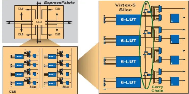
The basic structure of FPGA consists of wire matrices and configurable logic blocks (CLBs). The structure of CLBs is composed of look up tables (LUTs), flip flops and carry chain which is a dedicated wire connected to the LUT
*
This work was supported in part by the Higher Education Commission, Government of Pakistan.
FPGA Fabric Specific Optimization for RTL Design
Aqib Perwaiz1, Hamid M Kamboh2and Shoab A Khan3
1. Aqib Perwaiz is with the Computer Engineering Department College of E&ME, National University of Sciences and Technology (NUST), Pakistan (e-mail: [email protected]).
2. Shoab A Khan is with the Electrical Engineering Department, College of E&ME National University of Sciences and Technology (NUST), Pakistan (e-mail: [email protected]).
3. Hamid M kamboh, is with Center for Advanced Studies in Engineering, Islamabad, Pakistan. (e-mail: [email protected]).
Abstract
This paper proposes a technique custom to the optimization requirements suited for a particular family of Field Programmable Gate Arrays (FPGAs). As FPGAs have introduced reconfigurable black boxes there is a need to perform optimization across FPGAs slice fabric in order to achieve optimum performance. Though the Register Transfer Level (RTL) Hardware Descriptive Language (HDL) code should be technology independent but in many design instances it is imperative to understand the target technology especially once the target device embeds dedicated arithmetic blocks. No matter what the degree of optimization of the algorithm is, the configuration of target device plays an important role as far as the device utilization and path delays are concerned*
Index Terms: Field Programmable Gate Arrays (FPGA), Compression Tree, Bit Width Reduction, Look Ahead Pipelining.
output ports to generate high speed carry propagation as shown in Fig 1.
Fig 1 Virtex-5 configurable logic blocks (CLBs) comprise two slices.
Different combinational logics are realized by combination of LUTs having different data input and output patterns. Virtex 5 FPGA has six input and one output LUT, the single LUT can output one bit data from six bit input data, if this resource is properly used for the circuit design, it may be possible to obtain more compact and high performance circuit. Therefore it is imperative for circuits to be implemented in FPGA to consider the structure while designing and optimizing the algorithm.
Fig 2 DSP 48 slice in Vertex 5 FPGA
Xilinx with Virtex-5 DSP48 unit has a clock rate of 550 MHz and the precision of 25 x 18 bits as per fig 2. Xilinx has optimized the Virtex-5 DSP48 slice for adder chain implementations which is a powerful capability that enables the creation of very efficient high-performance filters [5].
After in detail study of the structure of Virtex 5 FPGA it is clear that the express fabric which has carry chain and six input LUT yield the most effective tradeoff between critical path delay which is the determining factor for logic fabric performance and die size. Due to the regular routing pattern of the express fabric the interconnectivity between six LUTs enhances performance by reaching more places in fewer hops. Any algorithm involving multiplication reduction technique can be implemented using 6:3 compression trees structure instead of 4:2 or 3:2 or any other, so that it is mapped efficiently onto the 6 LUTs
present in the FPGA and utilizing the faster interconnectivity yield minimum path delay.
Each DSP48 present in the FPGA can add three stages of pipelining in the multiply and accumulate (MAC) operation. If pipelining is not used these registers are bypassed, therefore addition of these pipeline stages improves the performance manifolds without causing any hardware overhead.
A. Compression Trees
Compression trees are used to add different partial products of a multiplication and eliminate the need for usage of dedicated multiplier hardware. For a known coefficient multiplication it is always desirable to use CSD to generate minimum partial products and further optimization is carried out by using different Wallace compression trees [4]. Traditionally the 4:2 Wallace tree has been considered the most efficient compression choice for VLSI design but in case of FPGAs the results depend upon the inherent LUT structure, as we have used Virtex 5 FPGA in our experiments that has 6:1 LUTs, therefore the choice of 6:3 compression tree outperforms that of others.
B. Multiplier Pipelining
DSP 48 block integral in Virtex 5 FPGAs is a multiply and accumulate block that has special hardware 18 x 25 bits multiplier and a 48 bit accumulator that has 3 input ports and 1 output port. The block has inherent 3 stages of pipelines as shown in fig 2. The inputs are pipelined through A and B registers (Regs), the multiplier and adder using M Reg and the output using P Reg. Thus any multiply accumulate operation can be pipelined efficiently up to a maximum of 4 levels without incurring any additional hardware overhead. These stages can effectively increase the throughput of a digital design ranging from 80 to 500 MHz [5].
C. Bit Width Optimization
Selection of bit resolution for algorithm implementation plays an interesting role as far as the hardware complexity, mean square error (MSE) and power consumption is concerned. Sometimes increasing the bit resolution has drastic effects on hardware complexity as compared to the decrease in MSE [8]. The used bit width when correlated with the underlying fabric structure of the FPGA yields some performance slots/bands. The design choice is therefore reduced to selection of one or the other architecture based upon optimization of the characteristics of user choice yielding minimum bit width and highest performance slot.
DESIGN OPTIMIZATIONS
To study the effects of the discussed hardware design optimizations three case studies were done, first a FIR filter [6] was implemented using direct, systolic and transformed
forms and then its CSD version was synthesized for study of different compression trees, secondly an IIR filter was implemented in direct and pipelined form applying look ahead transformation. The CSD version was also implemented to study different compression trees. Lastly a complex multiplier was synthesized using DSP 48, direct multiplication operation and the above discussed compression trees using booth coding for partial product generation.
A. FIR filter Optimization
A seven tap FIR filter DF-1 is shown in Fig.3.
X X X X
+
X X X
+ + + +
+
D D D D D D
X(n)
Y(n)
Fig 3 Seven tap FIR filter
The above filter was synthesized using Xilinx Virtex 5 device 5vlx220ff1760-2 and the design was found to be running at 73.678 MHz using 8 DSP48 blocks[9][10]. The systolic implementation of same filter effectively using the pipeline registers as per Fig 4 synthesized at 591.017 MHz which is 8 times faster utilizing the same hardware resources.
X X X X
+
X X X
+ + + +
+
D D D D D D
X(n)
Fig 4. Systolic Fir filter (dashed line represent cutset)
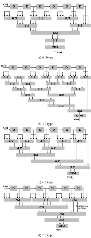
To analyze the effect of different architectures the same filter was re-implemented as CSD (canonic sign digit) using carry chain and carry save addition employing compression trees of 3:2, 4:2, 6:3 and 7:3 respectively. Schematic of different compression trees is shown in fig 5. The 4:2 compression tree is widely used for partial product reduction in ASICs, where as 6:3 and 7:3 compression trees have been custom designed to evaluate the suitability of the MAC for the specific FPGA architecture. CSD representation reduces the number of ones in a coefficient by about 33% [13] and keeping the CSD coefficients of the multiplier to 3 results in partial product reduction by 25% and a filter performance of 42 dBs.
D D D D D D
6:3
3:2 X(n)
Y(n)
6:3 6:3
6:3 6:3
6:3
CPA
a) 6: 3type
D D D D D D
Y(n) 3:2
3:2
CPA
3:2 3:2 3:2 3:2 3:2 3:2
3:2 3:2 3:2
3:2 3:2 3:2
3:2 3:2
3:2
3:2
3:2 X(n)
b) 3:2 type
D D D D D D
X(n)
Y(n)
4:2
CPA
4:2 4:2 4:2 4:2 4:2
4:2 4:2
4:2
3:2
c) 4:2 type
D D D D D D
X(n)
Y(n)
7:3
CPA
7:3 7:3 7:3
7:3 3:2
CORRECTION VECTOR
d) 7:3 type
Fig 5. Schematic of different compression trees
The CSD recoding is done using the following logic. Any number A can be represented in two’s compliment [3] form as follows.
/ / / / /
1. 2. 3.
...
1. 0w w w
A
a
a
a
a a
(1)The CSD representation of A is
a
w 1.a
w 2.a
w 3....
a a
1. 0 (2) The algorithm is as follows/
1
0
1
0
(4) / /1
w w
a
a
/ / 1
1 1
/ 1
(
0
1)
{
(1 2
) }
i i i
i i
i i i
for i
to W
a
a
a
a
(5)
B. IIR filter Optimization
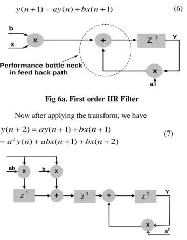
First order IIR filter[7][8] was also implemented in DF-1 realization. Due to the feedback loop inherent in the recursive part the filter architecture as per Fig 6a cannot be pipelined directly and requires employing look ahead transformation [2] to add pipeline stages to the filter. After the transformation as per Fig 6b the Synthesis of both the filters on the same deviceresulted in clock operating rates of 247.588 MHz and 370.157 MHz respectively.
y n( 1) ay n( ) bx n( 1) (6)
+
X
Z1
b
X Y
a Performance bottle neck
in feed back path x
Fig 6a. First order IIR Filter
Now after applying the transform, we have
2
( 2) ( 1) ( 1)
( ) ( 1) ( 2)
y n ay n bx n
a y n abx n bx n
(7)
Y
a2
ab
+ b
+ z-1
X X
X
z-1 z-2
Fig 6b. First order IIR filter after transformation
The Look Ahead transformation is applied by using the following generalized form
1
0
( ) ( ) ( 1 )
M
M i
i
y n M a y n a bu n M i (8)
After transformation the loop delay becomes m
Z
which was 1
Z before, which means that the loop iteration
is completed in M cycles and the system is approximately M times fast.
A. Complex Multiplier
Each complex multiplication operation involves four multiplications, one addition and a subtraction operation.
(9) and are the products for real and imaginary parts respectively.
c
d X
b
X a
X X
+
+
REAL PART
IMAGINARY PART
Fig 7. Complex multiplier
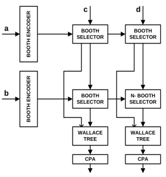
As these operations involve significant overhead than a normal multiplication operation, therefore, to implement complex multiplier that is suited for FPGA structure we resort to LUT based implementation utilizing fast carry chain. Booth algorithm is used for partial product generation and Wallace tree is utilized for partial product reduction. Booth coding reduces the partial products by half and then different compression trees are implemented for comparison of path delays and the LUTs used.
Fig 8. Wallace tree schematic
For the generation of partial products the Booth recoding algorithm[11] is used which results in reduction by roughly one half. The multiplication is carried out by scanning the operands from left to right. The multiplier A in two’s compliment representation is expressed by
2 1 1
0
2 ( 2 )j
n n
n j
j
A a a (10)
3 2 1 1 0 1
( 2 )2n k ... ( 2 )
n n n k
a a a a a a (11)
/ 2 1
2 2 1 2 ( 2 1) 0
( 2 )2
n
k
k k k
k
Here
a
n 1 represents the Sign bit, n is even, the product Y =CA is given by the following equation./ 2 1
2 2 1 2 ( 2 1) 0
( 2 )2
n
k
k k k
k
Y CA C a a a (13)
Encoding of consecutive two bits to a single bit by scanning three consecutive bits therefore reduces the number of partial products by half. Thus the overall architecture of optimized complex multiplier implementation comes out as:-
B
O
O
T
H
E
N
C
O
D
E
R
BOOTH SELECTOR
BOOTH SELECTOR
B
O
O
T
H
E
N
C
O
D
E
R
WALLACE TREE
WALLACE TREE
CPA CPA
BOOTH SELECTOR
N- BOOTH SELECTOR
a
b
c d
Fig. 9 Booth encoded Wallace tree reduction complex multiplier
4. EXPERIMENTAL RESULTS
The FIR and IIR filters were designed as shown in the Figs 5 and 6 by implementation of different compression trees. The design environment was as follows.
HDL : Verilog
Design Software: Xilinx ISE version 9.2.04i Simulator : Mentor graphics Modelsim SE6.1f Target Device: Virtex-5-XC5VLX220-2FF1760 A. FIR Filter
We have synthesized the filters by the parameters setting of optimization goal: speed and optimization effort: normal. In the synthesis tool the minimum clock period and the logic utilization are compared from the synthesis results. First we compare the FIR filter implementing normal, systolic, CSD and with different compression trees ratios.
B. IIR Filter
After that we compare the different forms of IIR filters, implementing normal, systolic, CSD and with different compression trees ratios.
Fig 10 FIR filter Comparison for the frequency (MHz) and number of utilized LUTs
Fig 11 IIR filter Comparison for the number of utilized LUTs and frequency (MHz).
Complex Multiplier
32 bit complex multiplier was synthesized with same optimization parameters. The number of LUTs used and the path delays are compared among different implementations of 4:2 compression trees, 6:3 compression tree, direct multiplication using multiplier operator, carry chain and hybrid implementations. As elaborated below in fig 12 the complex multiplier employing 6:3 compression trees in their Wallace tree reduction yielded minimum path delay with an acceptable number of LUTs used.
Fig 12 Comparison of LUTs and Path Delay of complex multiplier
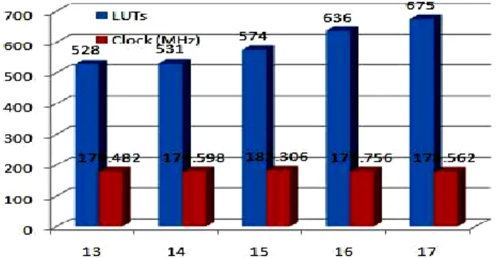
Bit Width Optimization
CSD implementation[12] of direct form FIR filter was synthesized for different bit widths of input and the filter
coefficients. The resulting clock speed and the LUTs are as shown in Fig 13.
Fig 13. LUTs and Clock rates for FIR filter.
The inherent design of the algorithm at 16 bits width if reduced to 15 shall result in 10% reduction in LUTs and 1.1% increase in clock speed. The implementation at a fixed point format of Q1.15 results in a Mean Square Error (MSE) of 0.0272 with a variance of 0.1704. Thereby indicationg an acceptable range for the operation for conservance of resources.
V. Conclusion
We have considered the optimization of key signal processing elements like FIR, IIR filters and complex multipliers, using FPGAs having CLBs comprising 6 LUTs. The design pays focus to the available resources and inherent fabric construction of a specific FPGA. It has been elaborated for different bit widths that 6:3 type compression is an efficient multiply add scheme as it is analogous to internal structure of FPGA, thus yields high speed and reduced area implementations. Further extension of the work can pave way for allocation of dedicated carry skipping support for the carry skip adder in FPGA fabric like the current technology of dedicated carry chains for carry propagate adders. It will produce FPGA implementations with even higher data rates and reduced die size to comparative implementations.
REFERENCES
[1] Xcell Journal “Achieve high performance with vertex 5 FPGA”,fourth quarter 2006.
[2] K.Satoh, J.Tada, H.Yanagida, and Y.tamura,”Parallel Image Reconstruction Operation By dedicated Hardware for three Dimensional Ultrasound Imaging”,pp.1522-1525, Proc of IEEE UFFC, Nov. 2007
[3] Keshab.k.parhi, “Pipelined and parallel recursive and adaptive filters” chapter 10 of pipelined adaptive digital filters
[4] Keshab.k.parhi, “Bit level Arithmetic architectures” chapter 13 of pipelined adaptive digital filters
[5] Vojin G. Oklobodzija, “The Computer Engineering Handbook”, CRC Press
[6] Anna Kuncheva and George Yanchev, “ Synthesis and implementation of DSP Algorithm in Advanced Programmable architectures” Proc of ISCCS 2008. [7] Antoli Sergyienko, Volodymir Lepekha, Juri Kanevski
and Przemyslaw Soltan, “ Implementation Of IIR Digital Filters In FPGA” Poland.
[8] Shanthala S and S.Y.Kulkarni, “Hight speed and low power FPGA Implementation Of FIR Filter for DSP Applications”,European Jounral of scientific research ISSN 1450-216x Vol.31 No.1(2009), PP. 19-28. [9] Xilinx Co.,:Xcell journal vol.58.59”,2007 Spring. [10] D.Phanthavong,”Designing with dsp 48 blocks using
precision synthesis,”Xcell Journal, 2005.
[11] Ki-seon Cho, Jong, Jin Seok, Goang Choi, “54x54 bit Radix 4 Multiplier based on modified booth algorithm”, ACM 2003 1-58113-677.
[12] Aqib Perwaiz and Shoab .A .Khan “ Effect of Bit Precision on hardware complexity for DDFS architecture”, IEEE Conference
BIOGRAPHIES
Aqib Perwaiz did his B.S.C Electrical Engineering from National University of Sciences and Technology, Rawalpindi. .He has 10+ years of experience in the area of hardware, software design and development along with expertise in fuel injection system optimization of Automobiles. His areas of expertise are embedded systems, ASIC design, Digital Signal Processing. He is currently pursuing his PhD in Computer Engineering from National University of Sciences and Technology Rawalpindi, Pakistan.
Dr. S. A. Khan did his PhD in Electrical and Computer Engineering from Georgia Institute of Technology; Atlanta, GA. Dr. Khan’s areas of specialization are Digital Signal Processing, Digital Design and Communication System. He has 12+ years industrial experience in companies like Scientific Atlanta, Picture Tel, and Cisco Systems. Mostly he worked on multi-DSP-based systems. As head of R&D group at Communications Enabling Technologies, he headed the team that executed a pioneering work of System on Chip (SoC) design. He is one of the five recipients of National Education Award 2001 in the category of Outstanding Services to Science and Technology.
Hamid M. Kamboh is a research student in CASE, Islamabad, Pakistan. The author has done BE (Avionics) in 1999, MS (Computer Engineering) in 2004 and working as a design engineer in helicopter technology. In the field of study of digital signal processing his specific research interests include Optimization in embedded systems focusing on the FPGAs and the filtering optimizations.