HIGH PRECISION MODELING OF GERMANIUM DETECTOR WAVEFORMS USING BAYESIAN MACHINE LEARNING
Benjamin E. Shanks
A dissertation submitted to the faculty at the University of North Carolina at Chapel Hill in partial fulfillment of the requirements for the degree of Doctor of Philosophy in the
Department of Physics.
Chapel Hill 2017
c
2017
ABSTRACT
Benjamin E. Shanks: High precision modeling of germanium detector waveforms using Bayesian machine learning
(Under the direction of John F. Wilkerson)
The universe as we see it today is dominated by matter, but the Standard Model of particle physics cannot explain why so little antimatter remains. If the neutrino is its own antiparticle – a so-called Majorana particle – lepton number must be violated, which is a key component of theories that explain the observed matter-antimatter asymmetry. Neutrinoless double-beta decay (0νββ), a hypothetical radioactive decay in certain nuclei, is the only experimentally accessible signature that can prove if neutrinos are Majorana in nature. But if it exists, 0νββ must be exceedingly rare, with current half-life limits over 1025 years. Measuring a process with such a faint signal requires extraordinary efforts to eliminate backgrounds. The Majorana Demonstrator is a search for 0νββ of germanium-76 in
an array of germanium detectors, with the goal of “demonstrating” backgrounds low enough to justify building a larger experiment with ∼1 tonne of isotope.
Reducing backgrounds even further will be critical to the discovery potential of a tonne scale experiment. One powerful method to reject background is pulse shape discrimination, which uses the shape of measured detector signals to differentiate between background and candidate 0νββ events. With a better understanding of pulse shapes from our detectors, we may be able to improve the discrimination efficiency. We have developed a detailed model of signal formation in germanium detectors, where the shape depends sensitively on characteristics specific to each individual detector crystal. To train the parameters for specific crystals in the Demonstrator, we have implemented a Bayesian machine
ACKNOWLEDGEMENTS
There are countless people whose support has made this dissertation possible. Thanks to my advisor, John Wilkerson, who allowed me the freedom to explore new ideas, the direction to bring them to fruition and a steady hand when things seemed hopeless. Chris O’Shaughnessy was the earliest and strongest supporter of this work, and it would never would have materialized without his encouragement and input. I’ve relied extensively on the work and germanium detector expertise of David Radford. Reyco Henning provided valuable advice and suggestions. Matt Green taught me how to be useful around a vacuum system. I have been fortunate to be surrounded many excellent Majorana collaborators, both to
learn from and to help pass the time in South Dakota.
Before coming back to physics, I spent a few years at General Electric. Mike Durling’s backing and advice came at a critical point in my career. Mauricio Castillo-Effen took me under his wing and introduced me to MCMC. Their influence on this work and my career can’t be understated.
TABLE OF CONTENTS
LIST OF TABLES . . . ix
LIST OF FIGURES . . . x
LIST OF ABBREVIATIONS AND SYMBOLS . . . xiii
1 Introduction . . . 1
1.1 Neutrinoless double beta decay . . . 1
1.2 The Majorana Demonstrator . . . 5
1.2.1 Initial results of the Majorana Demonstrator . . . 7
1.3 Signal modeling for germanium 0νββ experiments . . . 7
2 Modeling signal formation in germanium detectors . . . 15
2.1 Operating Principles . . . 15
2.1.1 Semiconductor detector design . . . 15
2.1.2 P-type point contact detectors . . . 18
2.1.3 Signal Formation: The Shockley-Ramo Theorem . . . 21
2.1.4 Pulse Shape Discrimination . . . 24
2.2 Signal Parameterization . . . 24
2.2.1 Detector Parameters . . . 27
2.2.2 Waveform Parameters . . . 39
2.3 Conclusion . . . 48
3 Machine learning of germanium detector parameters . . . 50
3.1 Bayesian modeling . . . 51
3.1.1 Markov chain Monte Carlo . . . 51
3.1.2 Diffusive nested sampling . . . 52
3.2 Learning model implementation . . . 55
3.2.1 Likelihood function . . . 56
3.2.2 Waveform parameterization and priors . . . 58
3.2.3 Detector and electronics parameterization and priors . . . 61
3.2.4 Sampling strategy . . . 72
3.3 Choosing a training set . . . 72
3.4 Conclusions . . . 82
4 Results & Applications . . . 83
4.1 Machine learning results . . . 83
4.1.1 Fit parameters . . . 85
4.1.2 Fit to second detector . . . 88
4.2 Validation . . . 90
4.3 Uncertainties . . . 102
4.4 Conclusions . . . 107
5 Conclusions . . . 110
5.2 Additional studies . . . 111
5.3 Improvements . . . 112
5.3.1 Model improvements . . . 112
5.3.2 Training improvements . . . 113
5.3.3 Computational improvements . . . 114
5.4 Outlook for theDemonstrator and beyond . . . 114
LIST OF TABLES
1.1 Summary of current 0νββ half life limits . . . 5
3.1 Summary of the free parameters in the model. . . 71
4.1 Training waveforms for detector P42661A . . . 85
4.2 Fit parameters for P42661A . . . 89
LIST OF FIGURES
1.1 Effective Majorana mass as a function of lightest neutrino mass . . . 3
1.2 Diagram comparing spectra for 2νββ and 0νββ . . . 5
1.3 Diagram of the Demonstrator shield . . . 8
1.4 Diagram of the Demonstrator detector unit . . . 9
1.5 Image of strings within a Demonstrator cryostat . . . 10
1.6 Preliminary spectrum for initialDemonstrator data . . . 11
1.7 0νββ 90% sensitivity as a function of background . . . 13
2.1 Schematic of a PPC detector . . . 19
2.2 Image of a PPC detector . . . 20
2.3 Schematic of a coaxial detector . . . 21
2.4 Weighting potential in a PPC detector . . . 22
2.5 Waveforms from multiple positions in a PPC detector . . . 23
2.6 Waveforms from single and multisite interactions . . . 25
2.7 Carrier drift velocity in Ge as a function of electric field and crystal axis . . 31
2.8 Band structure in germanium . . . 32
2.9 Constant-energy surfaces at germanium conduction band minima . . . 32
2.10 Constant-energy contours in germanium heavy-hole band . . . 34
2.11 Simulated effect of charge trapping on waveforms . . . 36
2.12 Simulated effect of trapped charge release on waveforms . . . 38
2.13 Comparison of various waveforms with same drift time . . . 39
2.14 Simulated effect of crystal axis orientation on waveforms . . . 40
2.15 Fractional risetime difference due to azimuthal velocity asymmetry . . . 41
2.16 Error introduced by cloud shape approximation with a gaussian convolution 43 2.17 The generalized gaussian shape for charge clouds . . . 44
2.19 Simulated effect of electronics shaping . . . 47
2.20 Bode diagram of preamp gain . . . 48
3.1 Illustration of diffusive nested sampling algorithm . . . 55
3.2 Digitized and windowed Demonstratorwaveforms . . . 57
3.3 Noise distribution of Demonstrator waveforms . . . 57
3.4 Time alignment of digitized waveforms . . . 60
3.5 Decaying tail of aDemonstrator waveform . . . 62
3.6 Fit to decaying tail of waveforms . . . 63
3.7 Low-pass transfer function parameterization . . . 65
3.8 Limits of velocity parameterization . . . 66
3.9 Electric field in PPC detector . . . 66
3.10 Histogram of electric field in PPC detector . . . 67
3.11 Reparameterized velocity curves . . . 68
3.12 Charge trapping effect on waveform amplitude . . . 71
3.13 Demonstratorcalibration track . . . 73
3.14 Demonstrator228Th calibration spectrum . . . 74
3.15 Current waveforms from 2614 keV photopeak . . . 75
3.16 Effect of A/E cut on 2614 keV photopeak . . . 76
3.17 Waveforms before and after A/E cut from 2614 keV photopeak . . . 77
3.18 Current waveforms of events which survive A/E cut . . . 78
3.19 Cut based on waveform baseline . . . 80
3.20 Distribution of drift times of single site events . . . 81
4.1 Training waveforms for detector P42661A . . . 84
4.2 Result of waveforms fit to detector P42661A . . . 86
4.3 Residuals of waveforms fit to detector P42661 . . . 87
4.5 Training waveforms for detector P2574A . . . 91
4.6 Residuals of waveforms fit to detector P2574A . . . 92
4.7 Fit likelihoods for waveforms from single and double escape peak . . . 94
4.8 Comparison of A/E and fit likelihood cut on the SEP and DEP . . . 95
4.9 Waveforms of DEP events in detector P42661A . . . 96
4.10 Positions estimated for DEP events in detector P42661A . . . 98
4.11 Simulated DEP event positions . . . 99
4.12 Azimuthal position estimated for DEP events . . . 100
4.13 Waveforms of DEP events in detector P42574A . . . 101
4.14 Positions estimated for DEP events in detector P42574A . . . 102
4.15 Histogram of Markov chain values for electronics parameters . . . 104
4.16 Histogram of Markov chain values for velocity parameters . . . 105
4.17 Histogram of Markov chain values for detector parameters . . . 106
LIST OF ABBREVIATIONS AND SYMBOLS
0νββ Neutrinoless Double-beta Decay 2νββ Double-beta Decay
A/E Current pulse amplitude to energy ratio BEGe Broad Energy Germanium
DEP Double Escape Peak DNS Diffusive Nested Sampling FET Field Effect Transistor HPGe High Purity Germanium LMFE Low Mass Front End MCMC Markov Chain Monte Carlo PPC P-type Point Contact PSD Pulse Shape Discrimination Q End-point Energy
ROI Region of Interest SEP Single Escape Peak
CHAPTER 1: Introduction
Section 1.1: Neutrinoless double beta decay
Determining the Majorana or Dirac nature of the neutrino is one of most important open challenges in neutrino physics. Unfortunately, any effect that would distinguish between them appears only at O(mν/E). Typical experiments fall in the regime mν/E 10−6 [1], making a measurement of the neutrino nature extremely difficult. The only signature of a Majorana mass currently considered feasible to detect is neutrinoless double-beta decay.
Two-neutrino double beta decay (2νββ) is a second order standard-model-allowed process observed in certain isotopes which have even numbers of both protons and neutrons. These “even-even” nuclei are sometimes more stable than neighboring odd-odd isotopes due to spin-pairing, which occurs independently for both protons and neutrons. In such an instance normalβ-decay is energetically forbidden, but Goeppert-Mayer [2] suggested in 1935 that a double beta decay ((A, Z)→(A, Z+ 2) + 2e−+ 2 ¯ve) might occur as a second order process with an extremely long half-life (> 1017 yr). A half century passed before the first direct laboratory measurement by Elliott et. al. of 2νββ in82Se [3], with a half life of 1.08×10²⁰ years.
Majorana nature of the neutrino therefore permits virtual neutrino exchange to mediate the 0νββ decay (A, Z)→(A, Z+ 2) + 2e−, violating lepton number by two units.
There are several different lepton number violating mechanisms which could mediate 0νββ. The scenario considered most likely is “light neutrino mediated” decay. If we assume the weak charged current is purely left handed and that either no unknown particles exist, or any unknown particles are too massive to contribute significantly to the 0νββ process, then the process is mediated only by the three light neutrinos. To first order, the half life of the light neutrino exchange 0νββ process is then given by [6]
T1/20ν−1 =G0ν|M0ν|2hmββi2 (1.1)
whereG0ν is a phase space factor,|M0ν| 2
the nuclear matrix element andhmββi 2
the effective Majorana mass, which is essentially an average of the mass states weighted by their mixing in the electron neutrino:
hmββi ≡
X i
Uei2mi
=c212c213m1+c213s 2
12m2ei2φ2 +s213m3ei2φ3
(1.2)
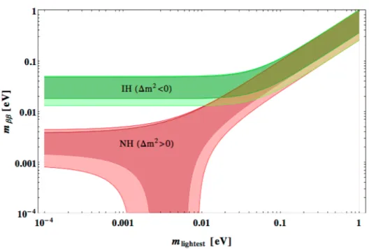
Here, Uei are the component of the Pontecorvo-Maki-Nakagawa-Sakata (PMNS) neutrino mixing matrix [7] that describes the composition of the electron neutrino in terms of the mass state mi. The Majorana phases, φ1 and φ2, are possible CP violating terms in the PMNS matrix for Majorana neutrinos (Dirac neutrinos have only one such phase). The terms sij and cij are the sine and cosine, respectively, of the mixing anglesθij of the PMNS matrix, as measured by neutrino oscillation experiments. The relationship between the lightest neutrino mass and mββ is shown in Figure 1.1. The effective Majorana mass, and therefore the half-life of 0νββ, depends sensitively on the neutrino masses, and especially on the neutrino mass ordering. A measurement of the half-life could, in turn, provide a measurement of the neutrino mass.
Figure 1.1: Effective Majorana mass plotted as a function of lightest neutrino mass for the cases of both normal (red) and inverted (green) mass ordering. The solid lines outline the allowed parameter space allowed from neutrino oscillation experiments, with uncertainties from neutrino mixing angles shown in the lighter color bands. Figure from [8].
the nuclear physics of the transition between the initial and daughter nucleii, and is not exactly calculable. The term can be written
M0ν =g2AM
(0ν), (1.3)
where gA is the axial vector coupling constant, and M(0ν) contains the contributions from the Fermi, Gamow-Teller and tensor operators for the transition [8].
focus of current theoretical efforts [10].
Multiple approximation method have been employed to calculate M(0ν), as reviewed in [10], notably the quasi-random phase approximation (QRPA), the interacting boson model (IBM) and the interacting shell model (ISM). However, there are a large number of virtual intermediate states available to the nucleus during the decay which increase computational complexity of the calculation. For a given 0νββ candidate nucleus, disagreement between calculations can vary by up to a factor of three – creating an order of magnitude uncertainty in the half-life, and further complicating comparison between experiments in different isotopes. The experimental signature of 0νββ is a peak in the energy spectrum at the endpoint energy of the decay (Qββ), as all the energy is shared between the pair of detected electrons. The 2νββ mode creates a continuous spectrum varying up to the endpoint of the decay. A simulated spectrum is shown in Figure 1.2. Typical measured half-lives for the 2νββ mode are around 1021 years, while the best limits for 0νββ have extended to 1025 years [11].
Given the extremely rare nature of the decay, 0νββexperiments must be constructed with a number of common design goals in mind. First, the largest possible mass of candidate iso-tope should be present. Many experiments are designed such that the source material forms the bulk of the detector. Backgrounds must be suppressed through radiopure construction materials, analytic signal rejection or both. In order to distinguish remaining backgrounds (including the irreducible 2νββ background) from signal, it is desirable to have good energy resolution in the region of interest around Qββ. A summary of experimental considerations is found in [6].
Figure 1.2: Spectra for 2νββ(dashed line) and 0νββ(solid line). Curves are drawn assuming the decay rate of 0νββ is 1% that of 2νββ, with a 2% resolution. Figure from [6].
Experiment Name Isotope Half life limit (×1025 y)
GERDA Phase II [12] 76Ge 4.0
CUORE-0 [13] 130Te 0.4
EXO-200 [14] 136Xe 1.1
KamLAND-Zen [15] 136Xe 10.7
Table 1.1: Summary of current 0νββ half life limits.
isotopic mass.
Section 1.2: The Majorana Demonstrator
The Majorana Demonstrator [16] is a search for neutrinoless double beta decay in
the isotope 76Ge. The experiment consists of an array of high purity germanium (HPGe) detectors of the p-type point contact (PPC) geometry. In total, there are 44.1 kg of detectors, of which 29.7 kg are 88% enriched in 76Ge. The main goal of the
Demonstrator is to
prove a germanium detector array can be constructed with sufficiently low background to justify investment in a tonne-scale germanium-76 0νββexperiment. Using the nuclear matrix element calculated with QRPA[17], a76Ge experiment must be sensitive to a half-life T0ν
1/2 ≈
The Demonstrator aims to achieve <3 counts/tonne-year in a 4-keV-wide region of interest (ROI) aroundQββ, which is 2039 keV for76Ge. Due to additional background reduc-tion from self-shielding and granularity cuts, this scales to<1 count/year for a tonne-scale experiment. The current design goal for a tonne tonne-scale experiment is 0.1 count/tonne-year in the ROI, which has been revised downward to ensure the inverted ordering region is covered for the worst-case nuclear matrix element calculations. In addition to showing the feasibility of a tonne-scale experiment, the Demonstrator will have a sensitivity to
T1/20ν ≈ 1026 yr. Using the same matrix element as above, this corresponds to mββ ≈ 100 meV.
The Demonstratorwas designed and constructed to achieve the lowest possible back-ground. Cosmic muon-induced signals are diminished by 4850’ of rock overburden above the experiment site at the Davis Campus of Sanford Underground Research Facility (SURF) in Lead, SD. An underground cleanroom lab facility was established with <500 particles/ft3. Parts within the cryostat, which therefore have a direct shine path to detectors, were main-tained in dry boxes purged with liquid nitrogen boil-off to minimize radon plate out. All detector manipulation took place in a ntirogen-purged glovebox with a particle count <10 particles/ft3. Radon levels and particle counts in the lab were carefully monitored before sensitive work proceeded.
Construction materials were chosen to ensure radiopurity. The majority of the cryostat material is composed of copper, which was manufactured with excellent chemical purity via electroforming. However, copper is cosmogenically activated, inducing long-lived radioactive isotopes, mainly 57Co and 60Co. To avoid cosmogenics, the
Majorana collaboration built
an underground electroforming facility where copper was grown starting in 2011. The copper was machined into parts in an underground shop staffed with a dedicated machinist.
The remaining layers are composed of lead and copper, with electroformed copper used for the innermost layer. A schematic of the shield is shown in Figure 1.3.
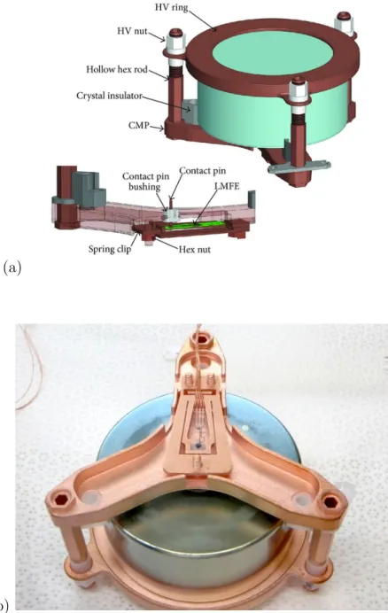
The Majoranadetector unit design is shown in Figure 1.4. The germanium crystal is
electrically isolated using plastic standoffs, which double as the thermal path for cooling. High voltage is applied via a copper contact ring, and signals are read out with a copper contact pin. A novel low noise low-mass front-end (LMFE) board [19] was designed to provide a resistive feedback readout. Since it is low mass and made of ultra pure materials, the LMFE can be placed near the detector, which minimizes stray capacitance. Three to five detectors are stacked into a “string” which shares a common thermal connection to a coldplate above. Each Majorana cryostat maintains cryogenic temperature and ultrahigh
vacuum for up to seven strings. Figure 1.5 contains an image of a fully loaded cryostat.
1.2.1: Initial results of the Majorana Demonstrator
TheDemonstratoris currently taking data with both modules in-shield. The collabo-ration has analyzed the first 32.4 days of data in this final configucollabo-ration, taken from August 25 to September 27, 2016, and constituting 1.39 years of isotopic exposure. The spectrum after preliminary analysis cuts is shown in Figure 1.6. For energies greater than ∼500 keV, the two neutrino spectrum dominates the spectrum. Given the low exposure of this dataset, we evaluate the background in a 400 keV wide window centered aroundQββ. After cuts, one background event remains in this window, which projects to 5.1+8.9−3.2 counts / (ROI·t·y) for a 2.9 keV ROI for module one detectors, and 2.6 keV ROI for module two detectors (where each ROI was chosen to optimize sensitivity given resolution at Qββ). This corresponds to a background index of 1.8×10⁻³ counts / (keV·t·y).
Section 1.3: Signal modeling for germanium 0νββ experiments
The Demonstrator is meant to show that we can achieve backgrounds low enough to
(a)
(b)
(a)
(b)
Figure 1.4: (a) A conceptual drawing of the Demonstratordetector unit. (b) Picture of
Figure 1.5: Image of strings hanging from a Demonstrator cryostat. Seven strings hang
Figure 1.6: Preliminary spectrum of initial Demonstrator data. The spectrum
encom-passes the first 1.39 kg·y of enriched detector exposure for the Demonstrator in its final
0νββ in the inverted ordering. In the case of a background-free experiment, the half-life sensitivity level S(T1/2) scales linearly with exposure,
S(T1/2)∝M ·t (1.4)
where M is the isotopic mass and t the total time over which data are collected. In the presence of background, due to poisson statistics, the sensitivity instead scales as a square root of exposure
S(T1/2)∝
r
M ·t
b·∆E (1.5)
where b is the background index and ∆E the size of the ROI. Figure 1.7 plots the rela-tionship between exposure and sensitivity for an enriched germanium, both for the case of a background-free experiment and for several background indexes. As we approach the ∼ 10 tonne-years of exposure necessary to cover the inverted ordering region, the background dramatically impacts the sensitivity level of the experiment. Given this reality, it is espe-cially important that the design of next generation experiments maximize the capability to discriminate against background with analysis cuts.
By developing an accurate model of signal formation in germanium detectors, we have two different paths to achieving lower background in a tonne scale experiment. During the design phase, we can use the model to create accurate simulated waveforms. These waveforms can be used to realistically evaluate the efficiency of analysis cuts against simulated backgrounds, and inform detector design to achieve maximal efficiency.
Exposure [ton-years]
3
−
10 10−2 10−1 1 10 102 103
90% Sensitivity [years]
1/2
T
24
10
25
10
26
10
27
10
28
10
29
10
30
10
range min
β β
IO m
Background free 0.1 counts/ROI-t-y
1.0 count/ROI-t-y
10 counts/ROI-t-y Ge (87% enr.)
76
ββ events and single-siteγ events.
Any analysis based on comparing waveforms to a model should, in principle, extract the maximal amount of available information about that waveform (assuming the model is accurate and exhaustive), optimized for the physical characteristics of specific detectors. When applied to background discrimination, this means a sufficiently accurate model should outperform simpler pulse shape heuristics. Furthermore, additional interesting information can be ascertained about waveforms, including the location of energy deposition within the detector volume.
In Chapter 2, we describe a model of signal formation in germanium detectors, and extend it specifically for the unique circumstances of the Demonstrator detectors. Chapter 3
CHAPTER 2: Modeling signal formation in germanium detectors
Section 2.1: Operating Principles
2.1.1: Semiconductor detector design
The interaction of radiation within a semiconductor material transfers energy from the incident particle to electrons bound in the atomic valence band. When the energy absorbed by an electron exceeds a threshold, the electron enters the conduction band and leaves behind a vacancy in the valence band, called a hole. Each hole is defined by the absence of an electron and therefore carries positive effective charge. Because the energy required to create an electron–hole pair in a semiconductor is very small (∼3 eV) [20], a large number of electron–hole pairs will be freed due to the interaction, creating a “cloud” of charge carriers. Both carrier types are free to drift through the material under the influence of an electric field, but in opposite directions due to their opposing charge. This feature allows the device to serve as a detector of the ionized signal.
measuring current spikes.
However, in a real world semiconductor sample, some population of elemental impurities will always occupy sites in the crystal lattice. Due to characteristics of their valence shell, some elements are able to donate an electron to the conduction band with an energy require-ment significantly less than the band gap. These impurities are called electron “donors”. Other impurities are prone to “accepting” electrons, thereby creating a hole in the conduc-tion band. If there is a net surplus of donor over acceptor impurities, the concentraconduc-tion of electrons at finite temperature naturally contains a surplus of electrons over holes, and is considered “n-type.” If the majority impurity type is acceptor, there are a surplus of holes, and the material is “p-type”. In either case, the contribution from impurities increases the net number of mobile charge carriers, and thereby lowers the resistivity by several orders of magnitude. Because of the low resistivity, if a voltage difference is applied across conducting contacts in the simple detector design described above, a large steady-state current will flow between electrodes.
To reduce the current, we can make use of the convenient property that semiconductors can be easily manufactured into diodes. A diode is “rectifying,” which means current flows freely when voltage is applied in the “forward” direction, but when “reverse” biased, almost no current flows. Diodes naturally form at the boundary betweennandptype regions within a semiconductor. If this junction is reverse biased, it can be operated as a detector with very little current flow.
exists is “depleted” of free charge carriers, because its majority carriers have recombined with stationary impurities.
If an external voltage is applied across the junction in a direction which reinforces the contact potential, it will attract electrons across the junction from the p region, and holes from then. In both cases, these are the minority carriers, and are very low in concentration. The material therefore exhibits very low conductivity and nearly no current will flow. On the other hand, if a voltage is applied opposite and greater than the contact potential, the majority carriers will again cross the junction, and current will flow freely. Thisp-njunction therefore behaves as a rectifying element. Holding thepside of the diode at positive voltage to then side constitutes forward biasing, and the opposite is reverse biasing. Increasing the reverse bias causes the depletion region to grow outward from the junction and deeper into the material. If the reverse bias reaches a critical level, the depleted region will break down and current will again flow rapidly.
The reverse biased diode is able to function as a detector because incident radiation can still generate new electron–hole pairs within the depleted region. In this case, the internal electric field produced by applied voltage and the impurity sites in the crystal, which have been ionized due to the external reverse bias, will force the minority carrier towards the junction. The depleted region therefore constitutes the active volume in which energy deposited by radiation can be collected.
extremely high concentration [21]. This high concentration layer is referred to as either p+ orn+ type, and generally serves as one of the detector electrodes. A detector manufactured from n-type crystal will have a thin p+ rectifying electrode, and one from a p-type crystal will have a thinn+ electrode.
Because the detector bulk is very high purity, an appreciable number of minority carriers will remain after depletion. To reduce steady-state leakage current from these carriers, the readout contact is highly doped with the impurities of the same type as the bulk crystal material. This highly doped region will have very low concentrations of the minority carrier. This is called a “noninjecting” electrode. As a junction of two similar-typed semiconductors, it does not rectify, and is an “ohmic” contact [22].
2.1.2: P-type point contact detectors
The P-type point contact (PPC) germanium detector geometry was developed to main-tain a low detector capacitance in a relatively large-volume design [23]. Detector capacitance is coupled to the electronic noise generated on the observed signal. Therefore, a low capac-itance detector is able to achieve low thresholds and retain high resolution at low energies. The detectors were originally designed to increase sensitivity to the low energy nuclear recoil from dark matter scattering, and PPC detector experiments have produced leading exclu-sion limits for low dark matter masses [24, 25]. The possibility of measuring coherent elastic neutrino–nucleus scattering has also been explored [26]. Stable operation has been achieved with thresholds at or below ∼ 500 eV [24, 27].
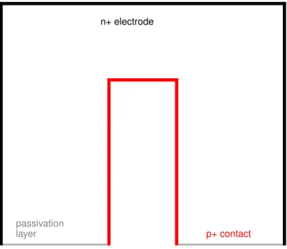
n+ electrode
p+ contact passivation layer
Figure 2.1: Cross-sectional schematic of the PPC detector geometry. The detectors are cylindrically symmetric, and produced with diameters around 6-7 cm, and axial lengths between roughly 3-5 cm. The p+ “point” contact is ∼2 mm in diameter. A positive bias of a few kilovolts is placed on the outern+ electrode, while the point contact is held at ground. The passivation layer reduces the flow of current along the detector surface.
treatment on the surface between the outer and point contact reduces current flow across the detector surface.
Figure 2.2: Picture of a PPC detector. The point contact is visible at the center of the top surface.
atmosphere, which further increases the material purity. The boule is then manufactured into detectors.
n+ electrode
p+ contact
passivation layer
Figure 2.3: Cross-sectional schematic of the coaxial germanium detector geometry. The p+ contact is bored several cm into the detector, which is ∼5-7 cm long.
2.1.3: Signal Formation: The Shockley-Ramo Theorem
As soon as a cloud of electron–hole pairs is created in the depleted region of a detector, they begin to drift under the influence of the electric field. This creates a current which, in turn, induces a current at the readout electrode. The generated signal therefore persists over the entire drift time of both charge carriers. In a PPC detector, holes will drift to the p+ point contact, and electrons towards the n+ outer contact. Because they are opposite charges drifting in opposite directions, they will each induce a net positive signal on the readout electrode.
−30 −20 −10 0 10 20 30 Radius (mm) 0 5 10 15 20 25 30 Height (mm) 0.0 0.2 0.4 0.6 0.8 1.0 W eighting P otential
Figure 2.4: Weighting potential for the point contact in a PPC detector. The point contact is located at bottom center, in the “dimple.” Black lines are “isochrones,” or lines of equal drift time for holes to reach the point contact. Each isochrone is spaced by 100 ns. The range of isochrones in this plot is from 100-700 ns.
every other electrode. By this definition, the weighting potential will always carry a value between zero and one. The Shockley-Ramo theorem then relates the total charge induced on the electrode, Q, as a carrier with charge q drifts through the weighting potential as a function of time:
Q(t) = q∆ϕ0(t) (2.1)
Given a model for charge carrier migration, the Shockley-Ramo theorem can be used to calculate the signal produced at the readout electrode.
0 200 400 600 800 0.00 0.25 0.50 0.75 1.00 Hole-Induced Cha rge [A.U.]
0 200 400 600 800
Time since charge creation [ns] 0.00 0.25 0.50 0.75 1.00 T otal Cha rge [A.U] 0 20
Radial position [mm] 0 10 20 30 Axial p osition [mm]
Figure 2.5: Simulated waveforms from eight points in a PPC detector. Positions are marked on the plot at right, which shows half a detector cross section. The shortest waveforms on left correspond to the marker closest to the point contact. The top left plot shows only the hole contribution, while the bottom shows the total contribution from both carriers.
2.1.4: Pulse Shape Discrimination
For neutrinoless double beta decay experiments, an important benefit of characteristic PPC waveform shape is that it enables discrimination between single and multiple point interactions [23]. A multisite interaction occurs when incident radiation deposits energy at more than one location in the detector, such as high energy gamma ray Compton scattering. Since a 0νββdecay deposits its energy within∼1 mm3, rejecting multisite events can reduce background signals.
Due to the long drift time and short collection time of PPC waveforms, charges deposited at different isochrones (see Figure 2.4) will have clearly time-separated signal components. In terms of the time dependence of the collected charge, the arrival of each new charge cloud generates a new “step” to a higher total charge, seen in Figure 2.6. By differentiating the collected charge and looking at current, each time–separated charge cloud appears as a distinct peak. Methods of multisite pulse shape discrimination in 0νββ experiments include cuts based on the energy-normalized amplitude of the current pulse [31] andχ2 comparison of each waveform to a set of known single site pulse shapes [32].
Section 2.2: Signal Parameterization
The Shockley-Ramo theorem provides a framework to calculate the detector response for any arbitrary signal in the detector. Calculating the weighting potential requires under-standing the detector geometry. Next, a model must be developed to simulate the position of charge carriers as a function of time. Understanding the drift path, in turn, requires a model for the electric fields in the detector and velocities of the charge carriers.
Figure 2.6: Charge (top) and current (bottom) signals formed by single and multisite in-teractions in a PPC detector. The left plots show a single site interaction with one smooth pulse, while the multisite waveform at right has “steps” in the charge pulse, and multiple peaks in the current pulse. Figure from [33].
This section describes the overall model used in this work. Parameters are sorted by three categories:
1. Detector Parameters: Affect the signal created at the electrode for every waveform simulated in a detector. Examples include detector dimension or drift mobility.
3. Electronics Parameters: Describe the shaping of waveforms by the electronics readout chain. Like detector parameters, these are common to all waveforms from the same detector.
A c software package developed within the GRETINA and Majorana collaborations
[34] forms the framework of this model. The weighting potential and electric field for a given set of detector parameters are calculated using a program called fieldgen. Both are calculated via numerical relaxation on a grid, set for this work to 0.1 mm, using the detector geometry described in Section 2.2.1. We assume azimuthal detector symmetry, and so the relaxation is performed over only the radial and axial dimensions. The weighting potential calculation solves the 2-D Laplace equation given boundary conditions of 1 on the n+ contact and 0 on the p+ point contact. The electric field calculation solves the 2-D Poisson equation, including the charge from ionized impurities using a model of impurity distribution described in 2.2.1. The n+ contact boundary condition is set to the detector operating voltage, and the point contact set to 0 V.
Using the output of fieldgen, siggen calculates charge trajectories for a given set of waveform and detector parameters. Given an initial position of energy deposition, siggen
calculates a drift velocity for the local electric field as described in Section 2.2.1. This velocity is used to determine the position after some time step ∆t, set for this work to 1 ns. The signal path is determined by iterating over a number of time steps until the charge reaches an electrode. The induced signal at the point contact is calculated for each time step by using the Shockley-Ramo theorem (Equation 2.1), where ∆ϕ0 is given by the difference in weighting potential at the final and initial position of the step.
It should be noted that fieldgen and siggen only attempt to model the detector bulk. Edge effects which are not modeled include reduced velocity for charges near the passivated surface and diffusion of charge across the n+-p boundary. These effects are only significant in waveforms with energy deposition ∼<1 mm from the detector surface.
incor-porated into a Python package called pysiggen[35]. Included in pysiggen are updates to the model for drift carrier velocities and electronics shaping. The python implementation provides several advantages, including rapid development and ease of interface with numer-ous external packages. By writing computationally intensive sections inc and wrapping into Python using cython [36], these advantages can be realized without sacrificing much in the way of computation time.
2.2.1: Detector Parameters Dimensions
The Majorana collaboration contracted AMETEK/ORTEC [37] to produce PPC
de-tectors for the Demonstrator using enriched 76Ge material. In order to maximize total
enriched detector mass cut from each crystal boule, ORTEC allowed the exact dimensions of each cylindrical detector to vary slightly. The typical mass is on the order of 1 kg, with diameters ranging from 60-70 mm and lengths from 40-50 mm. The point contact, located at bottom center of the detector, is recessed in a “dimple” with a radius and depth which vary from detector to detector by up to a millimeter. This dimple is modeled in fieldgen
as a hemispheroidal indentation. The outer diameter of each detector has a “taper,” a 45◦ chamfer on the bottom outside edges, which is nominally 4.5 mm in height. Finally, the top outside edges have a “bulletization” rounding radius, which is around 1.2 mm. Upon accep-tance of the detectors, Majoranacollaborators measured the detector dimensions using a high precision optical measuring device.
Impurities
Through the zone refinement and crystal pulling process described in Section 2.1.2, OR-TEC is able to create detectors with impurity concentrations on the order of 109 atoms per cubic centimeter. In general, the seed end of the crystal has higher impurity levels, and pulling the crystal introduces a gradient along the crystal length. The detector is manufac-tured in line with the direction of pulling, such that the impurity gradient aligns with the axial direction of the detector. The charge introduced by the impurities affects the electric field within the detector during operation. The gradient varies greatly between crystals, but is generally between ∼0.01−0.2×1010cm−4.
The siggen model used in this work allows for a linear impurity gradient, and assumes no radial impurity gradient. It is possible that a radial gradient is also present [38], but for successful crystal pulls at ORTEC, it is assumed this effect is negligible.
Impurities can be measured using the Hall effect, but the technique has relatively high uncertainties [21]. However, the impurity profile, together with the detector dimensions, determine the bias voltage at which the entire crystal volume depletes. The signals of a depleted and undepleted detector are significantly different, with the latter producing distinctly “rounded”, slower pulses due to diffusion in the undepleted region. Performing a careful characterization of the depletion voltage, and comparing to predicted depletion voltage for a given impurity profile, provides an independent check to the Hall measurements.
Operating Voltage
In general, germanium detectors are operated at some margin above the depletion voltage to ensure depletion, and to increase field strength and therefore drift velocity. Beyond the depletion voltage, field strength scales linearly with increased bias. Suggested operating voltages are supplied by ORTEC, which are applied to Demonstrator detectors with a
Drift Velocity
Accurately modeling signals in germanium detectors depends critically on understanding carrier drift velocities. Because the charges are propagating in a crystal, carrier mobilities are governed by the solid state physics of the system. This introduces nontrivial dependence of the drift velocity on both the magnitude of the electric field and the orientation of field with respect to the axes of crystal symmetry.
At low electric field and high temperature, the carrier drift velocity in germanium is Ohmic, meaning it increases linearly with electric field. In this regime, the velocity for each carrier is characterized by a mobilityµ0, where
~v =µ0E~ (2.2)
The drift velocity, ~v, will necessarily align with the electric field, E. As the energy of~ the carriers relative to the lattice temperature increases, scattering with the crystal lattice causes a deviation from Ohmic behavior [41]. This scattering causes the drift velocity to reach a point of saturation, such that the drift velocity becomes constant with increasing field. Carriers with energies high enough relative to the thermal energy of the crystal to deviate from Ohmic behavior are referred to as “hot” electrons or holes. Empirically, the high field drift velocity follows the form [42]:
v(E) = µ0E (1 + (E/E0)β)1/β
(2.3)
equation can describe germanium carrier mobilities at a range of temperatures [43].
In addition to scattering off the lattice, it is possible for carriers to scatter with charged crystal impurities [44, 45]. It is therefore possible for the observed parameters of Equation 2.3 to vary between germanium detector crystals even when operated at the same temperature.
Germanium has a diamond cubic lattice, with crystallographic basis vectors in the h100i,
h110iandh111idirections. The band structure (Figure 2.8) varies in energy depending upon the orientation of the wave vector ~k with respect to the crystal axis. At high fields, this generates an anisotropy in the induced carrier drift velocity, where the velocity magnitude varies depending on the orientation of the field. In addition, the induced current at high fields is no longer necessarily parallel to the electric field [48] 1. The details on how this arises are somewhat different for electrons, which propagate in the conduction band, and holes, which are affected by the valence band structure.
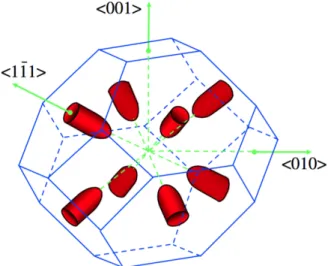
The lowest minima in the germanium conduction band are four ellipsoidal “valleys.” The long axis of each ellipsoid is aligned with anh111i crystallographic axis [50, 51], as shown in Figures 2.9. Electrons populating this minimum with a wave vector ~k parallel to the long axis have larger effective masses than those with a k value perpendicular to the axis, and therefore have reduced conductivity and contribute less to the current.
To understand how this generates misalignment between the field and current vector, consider first an electric field applied at some arbitrary angle with respect to a single ellipsoid. Because of the difference in mass, an electric field which is aligned with the small-mass ellipsoid axis will generate a larger current than one aligned in the large-massh111idirection. In addition, the higher conductivity in the small-mass direction causes the current vector to rotate somewhat toward the low-mass direction. Each of these effects is present regardless of the electric field strength.
102 103
4 6 8 10
V
elo
cit
y
[1E6
cm/s]
h100iholes h111iholes
102 103
Electric Field [V/cm] 4
6 8 10 12
V
elo
cit
y
[1E6
cm/s]
h100ielectrons h111ielectrons
Figure 2.8: Band structure in germanium. Curves indicate the energy associated with various bands as a function of wavevector. The conduction band minimum at h111i, labelled Eg, is associated with the ellipsoidal surfaces shown in Figure 2.9. At the valence band maximum enery, two degenerate bands meet, giving rise to hole populations with two distinct effective masses. The wider of the two is the so-called “heavy hole” band. Figure from [49].
the current vectors produced from each of the four minima. At low fields, cubic symmetry necessitates that the components misaligned with the field cancel, and the net current vector is parallel to the field. However, at high fields, the velocities of the electrons are high enough that behavior is no longer Ohmic. Electrons in ellipsoids for which the field is most aligned with the small-mass axis become hotter, and therefore have reduced mobilities compared to large-mass dominated valleys. This breaks the symmetry and results in a current which no longer aligns with the electric field [41]. The anisotropy is enhanced by “inter-valley” electron transfer with higher local minima in the band structure [53].
The situation for holes is somewhat more complicated due to the degeneracy in the valence band maximum, seen at~k = 0 in Figure 2.8. Two bands have the same ground state energy, but different shape, creating a situation in which ground state holes can have two different masses. The wider of the two bands has a higher effective mass and is labelled the “heavy” hole band. The shape of the heavy hole band, shown in Figure 2.10, is warped– spherical, with some dependence on crystal axis. The anisotropy produces effective masses which are largest in theh111i direction and smallest in the h100i. By the same argument as electrons above, this condition causes misalignment of the current and electric field vectors. The light hole band is almost perfectly spherical and does not significantly introduce anisotropic drift. In addition, at thermal equilibrium, the heavy holes makes up 96% of the hole population [41]. For these reasons, it is possible to model the hole transport using only the heavy hole band without significant loss of accuracy [54].
For fields aligned with crystallographic axes, rotational symmetry requires that the drift velocity aligns with field. However, the effect of the band structure described above causes decreased mobility for theh111icompared to theh100idirection, for both holes and electrons. Each axis can be then independently described by Equation 2.3. Fits to experimental data for holes and electrons along the h111iand h100i axes are shown in Figure 2.7.
Figure 2.10: Energy in the h110i plane of the heavy hole germanium valence band, shown with the solid line. The radial direction indicates valence band energy for the wavector at matching the polar angle. The dashed circle is included to emphasize deviations from a spherical structure. Figure from [54].
The hole drift velocity is therefore more important to model correctly. However, because of the complex valence band structure discussed above, precise calculation of the velocity for arbitrary field direction is difficult, and usually performed with computationally expensive Monte Carlo calculations [46]. To decrease calculation time in pysiggen, we have imple-mented an approximate model of hole velocity for fields with arbitrary crystal orientation first developed for gamma ray tracking experiments like AGATA [52]. Given the field ori-entation and velocity in theh111i and h100i directions, this model provides an approximate magnitude and direction for the velocity. The approximation is able to predict the h110i drift velocity to high accuracy.
We therefore require as input topysiggen six parameters to describe the hole velocities: the three parametersµ0, E0 andβ of Equation 2.3 for both theh111iandh100icrystal axes. This allows the flexibility to account for differences in drift velocity between detectors due to differences, for example, in temperature or impurity concentration.
With input of velocities in all three crystallographic directions, it performs polynomial in-terpolation to calculate field in a given orientation. The velocity values are taken from data collected in [43]. More precise models exist [47, 52] and could be implemented in the future. While it is possible this introduces percent-level error in waveform shape for events originat-ing near the point contact, in the crystal bulk we expect accuracy to the order of parts per ten thousand.
Charge Trapping and release
The presence of impurity sites and crystal defects introduces potential wells for charge carriers. It is possible for some carriers to become trapped at these sites as they drift through the detector. Charge that becomes trapped will no longer induce signal at the electrode, so trapping attenuates the observed pulse amplitude. This effect can be modeled in terms of a mean free drift time of charge carriers before encountering trapping [55].
In the assumed model, the magnitude of drifting charge is reduced by a constant fraction per unit time, resulting in an exponential attenuation in charge as a function of drift time:
q(t) = q0e−t/τT (2.4)
where q(t) is the time-dependent charge contained in the carrier cloud, q0 is the charge created in the initial interaction, and τT is the mean free drift time of trapping. We have implemented this model insiggen by reducing the effective charge of the charge cloud as a function of time. An example of waveforms generated with varying charge trapping constants is shown in Figure 2.11.
0 100 200 300 400 500 600 700 800 0.0
0.2 0.4 0.6 0.8 1.0
Cha
rge
[No
rm.
to
no
trapping]
No Trapping τT=5µs τT=10µs
0 100 200 300 400 500 600 700 800
Time since charge created [ns] 0.0
0.1
Residual
[A.U.]
waveform is reconstructed from the amplitude of the pulse, so charge trapping results in a degradation of energy resolution. This effect has been observed in the Demonstrator detectors with trapping constants on the order of hundreds of microseconds, corresponding to an energy reduction on the order of parts per thousand. The collaboration has developed a technique to correct the energy reconstruction which improves the resolution at 2614 keV by a factor as high as two.
Charges will eventually thermally escape from trapping sites. Release of trapped charge contributes a delayed current, resulting in a slow component of the signal. Like trapping, the release can be modeled in terms of an exponential time constant, τR. This effect is modeled very simply in pysiggen by summing the total current trapped charge and exponentially returning the charge to the cloud. During the drift time, the charge is added to the current location of the charge cloud, and not released at the point it was trapped. Once the charge cloud has reached the contact, amplitude is added to the signal exponentially until it reaches the amplitude expected for a signal with no trapping. The model is shown in Figure 2.12
This model for charge release is an imperfect approximation. A more complete model should re-inject charge at the point it was trapped. Doing so, however, would greatly increase the computational complexity of a waveform simulation.
0 250 500 750 1000 1250 1500 1750 2000 0.0
0.2 0.4 0.6 0.8 1.0
Cha
rge
[No
rm.
to
no
trapping]
No trapping τ=10µs
τT=10µs,τR=1µs
0 250 500 750 1000 1250 1500 1750 2000
Time since charge created [ns] 0.00
0.05
Residual
[A.U.]
2.2.2: Waveform Parameters
Interaction Position
Given a weighting potential, electric field, and drift velocity model, the generated signal for interactions for any a given position can be calculated. Both the drift path and total drift time of the charge cloud are obviously sensitive to the radial and axial position. To first order, the shape of the waveform is dominated by the hole drift time, and therefore the isochrone of origin. However, Figure 2.13 shows that there are percent-level differences in waveforms even along an isochrone.
0 100 200 300 400 500
0.00 0.25 0.50 0.75 1.00
Hole-Induced
Cha
rge
[A.U.]
0 100 200 300 400 500
Time since charge creation [ns]
−0.02 0.00 0.02
T
otal
Cha
rge
[A.U]
0 10 20 30
Radial position [mm]
0 5 10 15 20 25 30 Axial p osition [mm]
Figure 2.13: A comparison of shape between simulated waveforms with the same drift time (400 ns). Each event originates at azimuthal positionφ= 0, which corresponds to the h100i crystal axis. The position of each event, shown at right, corresponds with the waveform color at left. Residuals are drawn compared to a waveform from the position at right marked in black. Differences between the waveforms are at the part per hundred level, which originate because of differences in weighting potential and electric field along the drift path.
0 100 200 300 400 500 0.0
0.2 0.4 0.6 0.8 1.0
Hole-Induced
Cha
rge
[A.U.]
φ=0 rad
φ=π/8rad φ=π/4rad
0 100 200 300 400 500
Time since charge created [ns] 0.00
0.25
Residual
[A.U.]
Figure 2.14: Comparison between waveforms simulated at the same radial and axial position (r = 20, z = 20), but varying the azimuthal position. The crystal axis anisotropy in drift velocity at high electric field is responsible for the change in drift time. The fastest velocities occur along the h100i axis, corresponding to φ = 0, while the h110i axis corresponds with φ=π/4. Residuals are shown relative to the φ= 0 waveform.
h110i axis. The waveform is therefore sensitive to the azimuthal position of the event, but with an eight-fold degeneracy. An example of waveforms from the same position generated at different azimuthal positions is shown in Figure 2.14. The fractional difference in risetime, and therefore the residual difference, between waveforms from the h100i and h110i axis will vary as a function of position (Figure 2.15). In general, maximum residual differences are on the order of parts per hundred.
0 5 10 15 20 25 30 Radius (mm)
0 5 10 15 20 25 30
Height
(mm)
0.00 0.02 0.04 0.06 0.08 0.10 0.12 0.14
F
ractional
Drift
Time
Difference
Figure 2.15: Fractional difference in rise time calculated between events which occur at the
Energy
Assuming that all the charge generated in an event is collected, the signal amplitude depends linearly on energy. In pysiggen, the simulated signal is adjusted for energy before the charge trapping correction is applied. When incorporating the shaping of the electronics (see Section 2.2.3), all filters applied are corrected to preserve unity gain of the signal. By this procedure, the energy parameter remains a true measurement of energy, independent of any other parameter’s effect on amplitude.
Charge cloud size & shape
The size and shape of the ionization charge cloud created in the crystal varies depending on the type of particle interacting and the total energy deposited. After creation, the cloud size can further grow due to diffusion and self-repulsion. We assume this cloud is created spherical gaussian in nature, reflecting a point-like energy deposition2. As charges accelerate and decelerate, the cloud stretches in space, but remains roughly gaussian in time. Since the majority of signal is generated very near the point contact, we make the further approx-imation that the cloud size correction can be performed with a single gaussian convolution in the time domain. The gaussian sigma is parameterized in time, which corresponds to the spatial width via the final velocity of the charge.
This approximation was made to reduce computational complexity, but does not fully encapsulate the shape of the signal. To quantify the degree of error introduced, the true signal produced by spherical gaussian signal was created using Monte Carlo. A million random points were generated around the interaction point, with each of the r, φand z components and normally distributed with σ = 0.5 mm. A waveform was simulated for each of these points, and averaged to create a final signal. This was compared to the simplified gaussian convolution, choosing the gaussian sigma which minimized the least square difference from 2For radiation with longer interaction track lengths, such as MeV-scale electrons, the charge will be elongated
the Monte Carlo waveform. Figure 2.16 shows the result of this study. For realistic charge cloud sizes at any point in the detector, the calculated difference between the full Monte Carlo model and the simplified gaussian convolution is on the order of parts per thousand.
0 100 200 300 400 500 600
0.0 0.2 0.4 0.6 0.8 1.0
Hole
signal
[A.U.]
no smoothing Monte Carlo Gaussian Filter
0 100 200 300 400 500 600
Time since charge created [ns] 0.000
0.001
Residual
[A.U]
Figure 2.16: Measure of the error introduced by approximating the charge cloud shape as a gaussian convolution in the time domain of a single-point waveform. The red waveform shows the approximated waveform, while the blue waveform is the average of a set of many waveforms drawn from a spherical gaussian distribution around the same point. The residual below shows the difference between the Monte Carlo and Gaussian Filter waveforms.
In addition to the charge cloud size,pysiggen includes an optional parameter to modify the shape of the gaussian cloud. The spherical gaussian charge cloud assumes a point-like energy deposition. For events in which the energy despotion has some finite width, the charge cloud distribution should initially be more like a uniform sphere. However, diffusion as the cloud travels still spreads the charge in a gaussian manner. To combine the effects,
the cloud shape distribution such that the convolution weighting distributionw(t) becomes
w(t)∝exp −1 2
t σ
2p!
, (2.5)
where σ still controls the width, and p controls the shape. The usual gaussian distribution is recovered for p = 1 and, in the limit p → ∞, w(t) becomes a uniform distribution over (−σ, σ).See Figure 2.17 for examples of this distribution.
−60 −40 −20 0 20 40 60
0.0 0.2 0.4 0.6 0.8
1.0 p = 1.0
p = 1.2 p = 2.0 p = 5.0
Figure 2.17: Generalized gaussian charge cloud shape described in Section 2.2.2. The distri-bution of Equation 2.5 is drawn with σ= 20 for four different values of p.
2.2.3: Electronics Parameters
The Majorana collaboration designed an optimized detector electronics readout and
Figure 2.18: Schematic of theDemonstratorsignal readout chain. The low mass front end
(LMFE) board is located within the cryostat, very near to the detector point contact, as seen in Figure 1.4. The LMFE contains a resistive feedback element (RC element at top), field effect transistor with drain and source lines, and capacitively coupled pulser input (bottom). The four lines are bundles into one cable, which runs ∼2 m to additional amplification elements outside the shield. Figure from [33].
germanium resistor, called the “low mass front end” (LMFE) board [19]. The LMFE is lo-cated within a few millimeters of the detector, reducing stray input capacitance and therefore series noise. However, given this positioning, the LMFE hardware must be must be minimal and constructed only with very radiopure materials, while the rest of the preamplifier sys-tem is located outside of the cryostat. Approximately 2 m of 0.4 mm diameter cable runs between the LMFE and first stage of the preamplifier, thereby creating a feedback loop 4 m long. A second stage preamplifier, also outside the cryostat, is capacitively coupled to a second stage of amplification. The signal is then digitized with 14 bit precision at 100 MHz with GRETINA digitizer boards [56], which were originally developed for the GRETINA experiment.
FET, but the pulser input is also shaped by 2 meters of cable running into the cryostat. Without a direct measurement of the transfer function, we have developed an empirical parameterization.
The LMFE and inductance from the cable attenuate high frequency components of the signal, and can be modeled as a low-pass filter. A transfer function of order n can be generically modeled as a digital filter in the z domain
H(z) = cnz
n+cn−1zn−1+. . .+c0 dnzn+dn−1zn−1+. . .+d0
(2.6)
To determine which order was appropriate for the Demonstrator electronics, we
at-tempted to fit waveforms with a generic filter of first, second, and third order. Qualitatively, the second order filter was found to match the shape of the observed waveforms significantly better than a first order filter. The third order filter showed no dramatic improvement over the second order. For this reason, we chose to use a second order transfer function.
The fit to the second order preferred values of c0 near to zero, giving us a total digital filter function with four free parameters
Hlow(z) =
az2+bz
z2+ 2cz+d2. (2.7)
In the time domain, this corresponds to a convolution with a decaying oscillatory kernel,
H(t)∝e−tcos(ωt+φ), (2.8)
with the correspondence between the time and z domain is given by:
ω = cos−1c d
and φ = tan−1
ac−b a√d2−c2
0 200 400 600 800 1000 Time since charge created [ns]
0.0 0.2 0.4 0.6 0.8 1.0 V oltage [A.U.]
No electronics shaping With electronics shaping
Figure 2.19: Simulated effect of the electronics chain on waveform shape. Note that the risetime is increased by ∼100 ns.
The steady-state, or DC, gain for the filter is given by
lim z→1
az2+bz z2+ 2cz+d2 =
a+b
1 + 2c+d2 (2.10)
and therefore increasing the value ofa+bonly linearly scales the amplitude without otherwise affecting the shape.
Capacitative couplings, most notably between the first and second preamp stages, cause the waveform to exponentially decay. Empirically, we observe two strong coupling constants with different strength. We model this with three additional parameters describing a linear combination of two exponential decay functions:
Hhi(z) =c
z−1 z−exp(−τT
1)
+ (1−c) z−1 z−exp(−τT
2)
. (2.11)
Here, τ1 is set by the RC constant of the coupling between the first and second stage ampli-fiers, usually around 72µs, andτ2 is a∼2µs coupling we believe is intrinsic to the digitizer. The constant cexpresses the fractional mixing between the decay constants.
103 104 105 106 107 108
Frequency (rad/s) −40
−30 −20 −10 0
Amplitude
(dB)
Low-Pass Hi-Pass
Figure 2.20: Bode diagram of preamp gain using the model described in Section 2.2.3. The total gain (on this logarithmic plot) is the sum of the two curves.
Hhi. The shaping introduced by the electronics chain using this model, based on parameters observed in theDemonstrator, is shown in Figure 2.19. The length of cable in the feedback
loop is responsible for the dramatic increase in rise time [33]. A Bode diagram showing the frequency response is shown in Figure 2.20.
The process of digitizing can also change the shape of the recorded waveform. There is some inherent nonlinearity in the relationship between analog amplitude and digitally con-verted amplitude due to limitations of the analog-to-digital converters on board the digitizer. For the Demonstrator, this nonlinearity of the GRETINA digitizer has been studied and
shown to introduce no more than ≤ 1 ADC unit error for any given sample. Because this is less than the noise amplitude, which is several ADC units, we ignore nonlinearity in our model.
Section 2.3: Conclusion
to a readout electrode, where they are read by a data acquisition system. A model, based fundamentally on the Shockley-Ramo theorem, has been developed to calculate the signal induced at the electrode during charge collection. This model is parameterized to account for differences between PPC detectors. As an extension specific to the data acquisition system of the Majorana Demonstrator, an empirical representation of an electronics transfer
function has been added.
CHAPTER 3: Machine learning of germanium detector parameters
The parameters outlined in the previous chapter sufficiently encompass the physics of waveform generation to enable high precision modeling of PPC detector signals. However, successfully modeling any specific detector requires precise tuning of over a dozen parame-ters, many of which are either unknown or highly uncertain. In the absence of independent measurements, it is possible to gain understanding of parameters by studying observed wave-forms.
The shape of each waveform carries information about each of the detector parameters. In principle, if the model described above is sufficiently accurate, this information can be extracted by fitting the free model parameters to the waveform. This approach is limited, however, due to the presence of noise, the high dimensionality and high degree of correlation in the fit. When such a fit is performed on a single waveform, it tends to “overfit,” or select parameters which fit the current waveform well but can’t be used to fit additional waveforms.
To address this issue, we have developed an algorithm which pools the information from many waveforms in order to maximize the extracted knowledge about the parameters. Be-cause it can infer information from a large and unspecialized data set, we label this a machine learning algorithm. Specifically, we use the framework of Bayesian modeling [57], which al-lows us to separately model each waveform’s individual parameters while sharing common parameters related to the detector and electronics. The hierarchical model is trained to the data using Markov chain Monte Carlo (MCMC) [58].
Section 3.1: Bayesian modeling
A Bayesian model attempts to infer the probability of the value of a set of parameters, θ, given a data set x. We can write this asp(θ|x), which represents the probability density for θ conditional on the observation of x. The foundation of any Bayesian method is Bayes’ law [57]:
p(θ|x) = p(θ)p(x|θ)
p(x) , (3.1)
which expresses p(θ|x) (known as the posterior distribution) in terms of p(θ) (the prior dis-tribution), andp(x|θ) (the likelihood function). The prior is a distribution which represents the knowledge of θ before the measurement. The likelihood represents the probability of measuring x if the parameter set θ is true, and is computed using a model. The denomina-tor, p(x), is a constant normalization factor obtained by integrating over all possible values of θ. Since it is a constant, p(x) is only necessary to compare posteriors between models.
3.1.1: Markov chain Monte Carlo
Markov chain Monte Carlo (MCMC) is a method for numerically estimating a distribution by sampling from it via a random walk [57]. Given a starting point,θ0, the MCMC algorithm steps randomly through a sequence of values for the parameter θ1, θ2, . . . such that the sampling density of the parameter values converges to a “target” distribution. When used for Bayesian analysis, the posterior is chosen as the target distribution.
The algorithm is based on a “Markov chain,” meaning that the value selected for the nth sample, θ