AD8197
Rev. 0
Information furnished by Analog Devices is believed to be accurate and reliable. However, no responsibility is assumed by Analog Devices for its use, nor for any infringements of patents or other rights of third parties that may result from its use. Specifications subject to change without notice. No license is granted by implication or otherwise under any patent or patent rights of Analog Devices.
One Technology Way, P.O. Box 9106, Norwood, MA 02062-9106, U.S.A. Tel: 781.329.4700 www.analog.com
FEATURES
4 inputs, 1 output HDMI™/DVI links Enables HDMI 1.3-compliant receiver Pin-to-pin compatible with the AD8191
4 TMDS® channels per link
Supports 250 Mbps to 2.25 Gbps data rates Supports 25 MHz to 225 MHz pixel clocks
Equalized inputs for operation with long HDMI cables (20 meters at 2.25 Gbps)
Fully buffered unidirectional inputs/outputs Globally switchable, 50 Ω on-chip terminations Pre-emphasized outputs
Low added jitter
Single-supply operation (3.3 V) 4 auxiliary channels per link
Bidirectional unbuffered inputs/outputs Flexible supply operation (3.3 V to 5 V) HDCP standard compatible
Allows switching of DDC bus and 2 additional signals Multiple channel bundling modes
1× (4:1) HDMI/DVI link switch (default)
2× (8:1) TMDS channel and auxiliary signal switch 1× (16:1) TMDS channel and auxiliary signal switch Output disable feature
Reduced power dissipation Removable output termination Allows building of larger arrays Two AD8197s support HDMI/DVI dual-link Standards compatible: HDMI receiver, HDCP, DVI Serial (I2C® slave) and parallel control interface 100-lead, 14 mm × 14 mm LQFP, Pb-free package
APPLICATIONS
Multiple input displays Projectors
A/V receivers Set-top boxes
Advanced television (HDTV) sets
GENERAL DESCRIPTION
The AD8197 is an HDMI/DVI switch featuring equalized TMDS inputs and pre-emphasized TMDS outputs, ideal for systems with long cable runs. Outputs can be set to a high impedance state to reduce the power dissipation and/or to allow the construction of larger arrays using the wire-OR technique. Flexible channel bundling modes (for both the TMDS channels and the auxiliary signals) allow the AD8197 to be configured as a
FUNCTIONAL BLOCK DIAGRAM
LOW SPEED UNBUFFERED HIGH SPEED BUFFERED
AVCC DVCC AMUXVCC AVEE DVEE VTTO OP[3:0] AUX_COM[3:0] ON[3:0] + – 4 BIDIRECTIONAL I2C_SDA I2C_SCL I2C_ADDR[2:0] VTTI VTTI IP_A[3:0] IN_A[3:0] + – IP_B[3:0] IN_B[3:0] + – IP_C[3:0] IN_C[3:0] + – IP_D[3:0] IN_D[3:0] AUX_C[3:0] AUX_B[3:0] AUX_A[3:0] AUX_D[3:0] + – 4 4 4 4 4 4 4 4 4 4 4 4 EQ SWITCH CORE SWITCH CORE CONTROL LOGIC CONFIG INTERFACE 3 2 2 SERIAL PARALLEL P P _C H [1: 0] PP_ O T O PP_ O C L PP_ EQ PP_ EN PP_ PR E[ 1: 0] RESET PE 4 4 AD8197 0 647 1-0 01 Figure 1.
TYPICAL APPLICATION
DVD PLAYER GAME CONSOLE SET-TOP BOX MEDIA CENTER HDTV SET HDMI RECEIVER AD8197 04:20 06 471 -0 02Figure 2. Typical HDTV Application
4:1 single HDMI/DVI link switch, a dual 8:1 switch, or a single 16:1 switch.
The AD8197 is provided in a 100-lead LQFP, Pb-free, surface-mount package, specified to operate over the −40°C to +85°C temperature range.
PRODUCT HIGHLIGHTS
1. Supports data rates up to 2.25 Gbps, enabling 1080p deep color (12-bit color) HDMI formats, and greater than UXGA (1600 × 1200) DVI resolutions.
2. Input cable equalizer enables use of long cables at the input (more than 20 meters of 24 AWG cable at 2.25 Gbps). 3. Auxiliary switch routes a DDC bus and two additional signals
Comparable Parts
View a parametric search of comparable parts
Evaluation Kits
• AD8197 Evaluation Board
Documentation
Data Sheet• AD8197: 4:1 HDMI/DVI Switch with Equalization Data Sheet
Reference Materials
Informational• Advantiv™ Advanced TV Solutions Technical Articles
• Analysis of Common Failures of HDMI CT • Video Portables and Cameras Get HDMI Outputs
Design Resources
• AD8197 Material Declaration • PCN-PDN Information • Quality And Reliability • Symbols and FootprintsDiscussions
View all AD8197 EngineerZone Discussions
Sample and Buy
Visit the product page to see pricing options
Technical Support
Submit a technical question or find your regional support number
* This page was dynamically generated by Analog Devices, Inc. and inserted into this data sheet. Note: Dynamic changes to the content on this page does not constitute a change to the revision number of the product data sheet. This content may be
TABLE OF CONTENTS
Features ... 1
Applications... 1
General Description ... 1
Functional Block Diagram ... 1
Typical Application... 1
Product Highlights ... 1
Revision History ... 2
Specifications... 3
Absolute Maximum Ratings... 5
Thermal Resistance ... 5
Maximum Power Dissipation ... 5
ESD Caution... 5
Pin Configuration and Function Descriptions... 6
Typical Performance Characteristics ... 9
Theory of Operation ... 13
Introduction ... 13
Input Channels... 13
Output Channels ... 13
High Speed (TMDS) Switching Modes ... 14
Auxiliary Switch... 14
Auxiliary (Low Speed) Switching Modes ... 15
Serial Control Interface... 16
Reset ... 16
Write Procedure... 16
Read Procedure... 17
Switching/Update Delay ... 17
Parallel Control Interface ... 18
Serial Interface Configuration Registers ... 19
High Speed Device Modes Register... 19
Auxiliary Device Modes Register... 20
Receiver Settings Register ... 22
Input Termination Pulse Register 1 and Register 2 ... 22
Receive Equalizer Register 1 and Register 2 ... 22
Transmitter Settings Register... 22
Parallel Interface Configuration Registers ... 23
High Speed Device Modes Register... 23
Auxiliary Device Modes Register... 23
Receiver Settings Register ... 24
Input Termination Pulse Register 1 and Register 2 ... 24
Receive Equalizer Register 1 and Register 2 ... 24
Transmitter Settings Register... 24
Application Information... 25
Pinout... 25
Cable Lengths and Equalization... 25
PCB Layout Guidelines... 26
Outline Dimensions ... 30
Ordering Guide ... 30
REVISION HISTORY
SPECIFICATIONS
TA = 27°C, AVCC = 3.3 V, VTTI = 3.3 V, VTTO = 3.3 V, DVCC = 3.3 V, AMUXVCC = 5 V, AVEE = 0 V, DVEE = 0 V, differential input
swing = 1000 mV, TMDS outputs terminated with external 50 Ω resistors to 3.3 V, unless otherwise noted. Table 1.
Parameter Conditions/Comments Min Typ Max Unit
DYNAMIC PERFORMANCE
Maximum Data Rate (DR) per Channel NRZ 2.25 Gbps
Bit Error Rate (BER) PRBS 223 − 1 10−9
Added Deterministic Jitter DR ≤ 2.25 Gbps, PRBS 27 − 1, EQ = 12 dB 25 ps (p-p)
Added Random Jitter 1 ps (rms)
Differential Intrapair Skew At output 1 ps
Differential Interpair Skew1 At output 40 ps
EQUALIZATION PERFORMANCE
Receiver (Highest Setting)2 Boost frequency = 825 MHz 12 dB
Transmitter (Highest Setting)3 Boost frequency = 825 MHz 6 dB
INPUT CHARACTERISTICS
Input Voltage Swing Differential 150 1200 mV
Input Common-Mode Voltage (VICM) AVCC − 800 AVCC mV
OUTPUT CHARACTERISTICS
High Voltage Level Single-ended high speed channel AVCC − 10 AVCC + 10 mV
Low Voltage Level Single-ended high speed channel AVCC − 600 AVCC − 400 mV
Rise/Fall Time (20% to 80%) 75 135 200 ps
INPUT TERMINATION
Resistance Single-ended 50 Ω
AUXILIARY CHANNELS
On Resistance, RAUX 100 Ω
On Capacitance, CAUX DC bias = 2.5 V, ac voltage = 3.5 V, f = 100 kHz 8 pF
Input/Output Voltage Range DVEE AMUXVCC V
POWER SUPPLY
AVCC Operating range 3 3.3 3.6 V
QUIESCENT CURRENT
AVCC Outputs disabled 30 40 44 mA
Outputs enabled, no pre-emphasis 48 60 64 mA
Outputs enabled, maximum pre-emphasis 88 100 110 mA
VTTI Input termination on4 5 40 54 mA
VTTO Output termination on, no pre-emphasis 35 40 46 mA
Output termination on, maximum pre-emphasis 72 80 90 mA
DVCC 3.2 7 8 mA
AMUXVCC 0.01 0.1 mA
POWER DISSIPATION
Outputs disabled 115 271 361 mW
Outputs enabled, no pre-emphasis 384 574 671 mW
Outputs enabled, maximum pre-emphasis 704 910 1050 mW
TIMING CHARACTERISTICS
Switching/Update Delay High speed switching register: HS_CH 200 ms
All other configuration registers 1.5 ms
Parameter Conditions/Comments Min Typ Max Unit
SERIAL CONTROL INTERFACE5
Input High Voltage, VIH 2 V
Input Low Voltage, VIL 0.8 V
Output High Voltage, VOH 2.4 V
Output Low Voltage, VOL 0.4 V
PARALLEL CONTROL INTERFACE
Input High Voltage, VIH 2 V
Input Low Voltage, VIL 0.8 V
1 Differential interpair skew is measured between the TMDS pairs of a single link.
2 AD8197 output meets the transmitter eye diagram as defined in the DVI Standard Revision 1.0 and the HDMI Standard Revision 1.3. 3 Cable output meets the receiver eye diagram mask as defined in the DVI Standard Revision 1.0 and the HDMI Standard Revision 1.3.
4 Typical value assumes only the selected HDMI/DVI link is active with nominal signal swings and that the unselected HDMI/DVI links are deactivated. Minimum and
maximum limits are measured at the respective extremes of input termination resistance and input voltage swing.
ABSOLUTE MAXIMUM RATINGS
Table 2.
Parameter Rating
AVCC to AVEE 3.7 V
DVCC to DVEE 3.7 V
DVEE to AVEE ±0.3 V
VTTI AVCC + 0.6 V
VTTO AVCC + 0.6 V
AMUXVCC 5.5 V
Internal Power Dissipation 2.2 W
High Speed Input Voltage AVCC − 1.4 V < VIN <
AVCC + 0.6 V High Speed Differential Input Voltage 2.0 V
Low Speed Input Voltage DVEE − 0.3 V < VIN <
AMUXVCC + 0.6 V I2C and Parallel Logic Input Voltage DVEE − 0.3 V < VIN <
DVCC + 0.6 V
Storage Temperature Range −65°C to +125°C
Operating Temperature Range −40°C to +85°C
Junction Temperature 150°C
Stresses above those listed under Absolute Maximum Ratings may cause permanent damage to the device. This is a stress rating only; functional operation of the device at these or any other conditions above those indicated in the operational section of this specification is not implied. Exposure to absolute maximum rating conditions for extended periods may affect device reliability.
THERMAL RESISTANCE
θJA is specified for the worst-case conditions: a device soldered
in a 4-layer JEDEC circuit board for surface-mount packages. θJC is specified for no airflow.
Table 3. Thermal Resistance
Package Type θJA θJC Unit
100-Lead LQFP 56 19 °C/W
MAXIMUM POWER DISSIPATION
The maximum power that can be safely dissipated by the AD8197 is limited by the associated rise in junction temperature. The maximum safe junction temperature for plastic encapsulated devices is determined by the glass transition temperature of the plastic, approximately 150°C. Temporarily exceeding this limit may cause a shift in parametric performance due to a change in the stresses exerted on the die by the package.
Exceeding a junction temperature of 175°C for an extended period can result in device failure. To ensure proper operation, it is necessary to observe the maximum power rating as determined by the coefficients in Table 3.
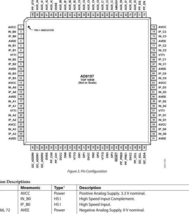
PIN CONFIGURATION AND FUNCTION DESCRIPTIONS
PP_ O T O AUX _A0 AUX _A1 AUX _A2 AUX _A3 D VEE AUX _B0 AUX _B1 AUX _B2 AUX _B3 AUX _CO M 0 AUX _CO M 1 AUX _CO M 2 AUX _CO M 3 AUX _C0 AUX _C1 AUX _C2 AUX _C3 A M U XVC C AUX _D0 AUX _D1 AUX _D2 AUX _D3 PP_ EQ PP_ EN 26 I2 C_ADDR0 27 I2 C_ADDR 1 28 I2 C_ADDR2 29 D VEE 30 PP_ C H 0 31 PP _C H 1 32 DV C C 33 ON 0 34 OP 0 35 VT T O 36 ON 1 37 OP 1 38 DV C C 39 ON 2 2 IN_B0 3 IP_B0 4 AVEE 7 VTTI 6 IP_B1 5 IN_B1 1 AVCC 8 IN_B2 9 IP_B2 10 AVEE 12 IP_B3 13 AVCC 14 IN_A0 15 IP_A0 16 AVEE 17 IN_A1 18 IP_A1 19 VTTI 20 IN_A2 21 IP_A2 22 AVCC 23 IN_A3 24 IP_A3 25 AVEE 11 IN_B3 74 IP_C3 AVCC 73 IN_C3 72 AVEE 69 VTTI 70 IN_C2 71 IP_C2 75 68 IP_C1 67 IN_C1 66 AVEE 64 IN_C0 63 AVCC 62 IP_D3 61 IN_D3 60 AVEE 59 IP_D2 58 IN_D2 57 VTTI 56 IP_D1 55 IN_D1 54 AVCC 53 IP_D0 52 IN_D0 51 AVEE 65 IP_C0 40 OP 2 41 VT T O 42 ON 3 43 OP 3 44 R ESET 45 PP _P R E 0 46 PP _P R E 1 47 DV C C 48 PP _O C L 49 I2 C _S C L 50 I2 C _S D A100 99 98 97 96 95 94 93 92 91 90 89 88 87 86 85 84 83 82 81 80 79 78 77 76
PIN 1 INDICATOR
AD8197 TOP VIEW (Not to Scale)
0
64
71
-00
3
Figure 3. Pin Configuration
Table 4. Pin Function Descriptions
Pin No. Mnemonic Type1 Description
1, 13, 22, 54, 63, 75 AVCC Power Positive Analog Supply. 3.3 V nominal.
2 IN_B0 HS I High Speed Input Complement.
3 IP_B0 HS I High Speed Input.
4, 10, 16, 25, 51, 60, 66, 72 AVEE Power Negative Analog Supply. 0 V nominal.
5 IN_B1 HS I High Speed Input Complement.
6 IP_B1 HS I High Speed Input.
7, 19, 57, 69 VTTI Power Input Termination Supply. Nominally connected to AVCC.
8 IN_B2 HS I High Speed Input Complement.
9 IP_B2 HS I High Speed Input.
11 IN_B3 HS I High Speed Input Complement.
12 IP_B3 HS I High Speed Input.
14 IN_A0 HS I High Speed Input Complement.
15 IP_A0 HS I High Speed Input.
17 IN_A1 HS I High Speed Input Complement.
18 IP_A1 HS I High Speed Input.
20 IN_A2 HS I High Speed Input Complement.
21 IP_A2 HS I High Speed Input.
Pin No. Mnemonic Type1 Description
24 IP_A3 HS I High Speed Input.
26 I2C_ADDR0 Control I2C Address 1st LSB.
27 I2C_ADDR1 Control I2C Address 2nd LSB.
28 I2C_ADDR2 Control I2C Address 3rd LSB.
29, 95 DVEE Power Negative Digital and Auxiliary Multiplexer Power Supply. 0 V nominal.
30 PP_CH0 Control Quad Switching Mode High Speed Source Selection Parallel Interface LSB.
31 PP_CH1 Control Quad Switching Mode High Speed Source Selection Parallel Interface MSB.
32, 38, 47 DVCC Power Positive Digital Power Supply. 3.3 V nominal.
33 ON0 HS O High Speed Output Complement.
34 OP0 HS O High Speed Output.
35, 41 VTTO Power Output Termination Supply. Nominally connected to AVCC.
36 ON1 HS O High Speed Output Complement.
37 OP1 HS O High Speed Output.
39 ON2 HS O High Speed Output Complement.
40 OP2 HS O High Speed Output.
42 ON3 HS O High Speed Output Complement.
43 OP3 HS O High Speed Output.
44 RESET Control Configuration Registers Reset. Normally pulled up to AVCC.
45 PP_PRE0 Control High Speed Pre-Emphasis Selection Parallel Interface LSB.
46 PP_PRE1 Control High Speed Pre-Emphasis Selection Parallel Interface MSB.
48 PP_OCL Control High Speed Output Current Level Parallel Interface.
49 I2C_SCL Control I2C Clock.
50 I2C_SDA Control I2C Data.
52 IN_D0 HS I High Speed Input Complement.
53 IP_D0 HS I High Speed Input.
55 IN_D1 HS I High Speed Input Complement.
56 IP_D1 HS I High Speed Input.
58 IN_D2 HS I High Speed Input Complement.
59 IP_D2 HS I High Speed Input.
61 IN_D3 HS I High Speed Input Complement.
62 IP_D3 HS I High Speed Input.
64 IN_C0 HS I High Speed Input Complement.
65 IP_C0 HS I High Speed Input.
67 IN_C1 HS I High Speed Input Complement.
68 IP_C1 HS I High Speed Input.
70 IN_C2 HS I High Speed Input Complement.
71 IP_C2 HS I High Speed Input.
73 IN_C3 HS I High Speed Input Complement.
74 IP_C3 HS I High Speed Input.
76 PP_EN Control High Speed Output Enable Parallel Interface.
77 PP_EQ Control High Speed Equalization Selection Parallel Interface.
78 AUX_D3 LS I/O Low Speed Input/Output.
79 AUX_D2 LS I/O Low Speed Input/Output.
80 AUX_D1 LS I/O Low Speed Input/Output.
81 AUX_D0 LS I/O Low Speed Input/Output.
82 AMUXVCC Power Positive Auxiliary Multiplexer Supply. 5 V typical.
83 AUX_C3 LS I/O Low Speed Input/Output.
84 AUX_C2 LS I/O Low Speed Input/Output.
85 AUX_C1 LS I/O Low Speed Input/Output.
86 AUX_C0 LS I/O Low Speed Input/Output.
87 AUX_COM3 LS I/O Low Speed Common Input/Output.
88 AUX_COM2 LS I/O Low Speed Common Input/Output.
Pin No. Mnemonic Type1 Description
90 AUX_COM0 LS I/O Low Speed Common Input/Output.
91 AUX_B3 LS I/O Low Speed Input/Output.
92 AUX_B2 LS I/O Low Speed Input/Output.
93 AUX_B1 LS I/O Low Speed Input/Output.
94 AUX_B0 LS I/O Low Speed Input/Output.
96 AUX_A3 LS I/O Low Speed Input/Output.
97 AUX_A2 LS I/O Low Speed Input/Output.
98 AUX_A1 LS I/O Low Speed Input/Output.
99 AUX_A0 LS I/O Low Speed Input/Output.
100 PP_OTO Control High Speed Output Termination Selection Parallel Interface.
TYPICAL PERFORMANCE CHARACTERISTICS
TA = 27°C, AVCC = 3.3 V, VTTI = 3.3 V, VTTO = 3.3 V, DVCC = 3.3 V, AMUXVCC = 5 V, AVEE = 0 V, DVEE = 0 V, differential input
swing = 1000 mV, TMDS outputs terminated with external 50 Ω resistors to 3.3 V, pattern = PRBS 27 − 1, data rate = 2.25 Gbps, unless
otherwise noted.
REFERENCE EYE DIAGRAM AT TP1
DIGITAL PATTERN GENERATOR
AD8197 EVALUATION
BOARD
SERIAL DATA ANALYZER
SMA COAX CABLE HDMI CABLE
TP1 TP2 TP3 064
70
-00
4
Figure 4. Test Circuit Diagram for RX Eye Diagram
0.125UI/DIV AT 2.25Gbps
250
mV
/D
IV
06
47
1-0
05
Figure 5. RX Eye Diagram at TP2 (Cable = 2 meters, 30 AWG)
0.125UI/DIV AT 2.25Gbps
250
mV
/D
IV
06
47
1-0
06
Figure 6. RX Eye Diagram at TP2 (Cable = 20 meters, 24 AWG)
0.125UI/DIV AT 2.25Gbps
250
mV
/D
IV
06
47
1-0
07
Figure 7. RX Eye Diagram at TP3, EQ = 6 dB (Cable = 2 meters, 30 AWG)
0.125UI/DIV AT 2.25Gbps
250
mV
/D
IV
06
47
1-0
08
TA = 27°C, AVCC = 3.3 V, VTTI = 3.3 V, VTTO = 3.3 V, DVCC = 3.3 V, AMUXVCC = 5 V, AVEE = 0 V, DVEE = 0 V, differential input
swing = 1000 mV, TMDS outputs terminated with external 50 Ω resistors to 3.3 V, pattern = PRBS 27 − 1, data rate = 2.25 Gbps, unless
otherwise noted.
REFERENCE EYE DIAGRAM AT TP1
DIGITAL PATTERN GENERATOR
SMA COAX CABLE
HDMI CABLE
TP1 TP2 TP3
AD8197
EVALUATION BOARD
SERIAL DATA ANALYZER
06
47
0-0
09
Figure 9. Test Circuit Diagram for TX Eye Diagrams
0.125UI/DIV AT 2.25Gbps
250
mV
/D
IV
06
47
1-0
10
Figure 10. TX Eye Diagram at TP2, PE = 2 dB
0.125UI/DIV AT 2.25Gbps
250
mV
/D
IV
06
47
1-0
11
Figure 11. TX Eye Diagram at TP2, PE = 6 dB
0.125UI/DIV AT 2.25Gbps
250
mV
/D
IV
06
47
1-0
12
Figure 12. TX Eye Diagram at TP3, PE = 2 dB (Cable = 2 meters, 30 AWG)
0.125UI/DIV AT 2.25Gbps
250
mV
/D
IV
06
47
1-0
13
TA = 27°C, AVCC = 3.3 V, VTTI = 3.3 V, VTTO = 3.3 V, DVCC = 3.3 V, AMUXVCC = 5 V, AVEE = 0 V, DVEE = 0 V, differential input
swing = 1000 mV, TMDS outputs terminated with external 50 Ω resistors to 3.3 V, pattern = PRBS 27 − 1, data rate = 2.25 Gbps, unless
otherwise noted.
0.5 0.6
0
0 25
HDMI CABLE LENGTH (m)
D E TE R M IN IS T IC J ITT E R ( U I) 0.4 0.3 0.2 0.1
5 10 15 20
2m CABLE = 30AWG 5m TO 20m CABLES = 24AWG
1.65Gbps EQ = 12dB 2.25Gbps EQ = 12dB
2.25Gbps EQ = 6dB
1.65Gbps EQ = 6dB
06
471
-01
4
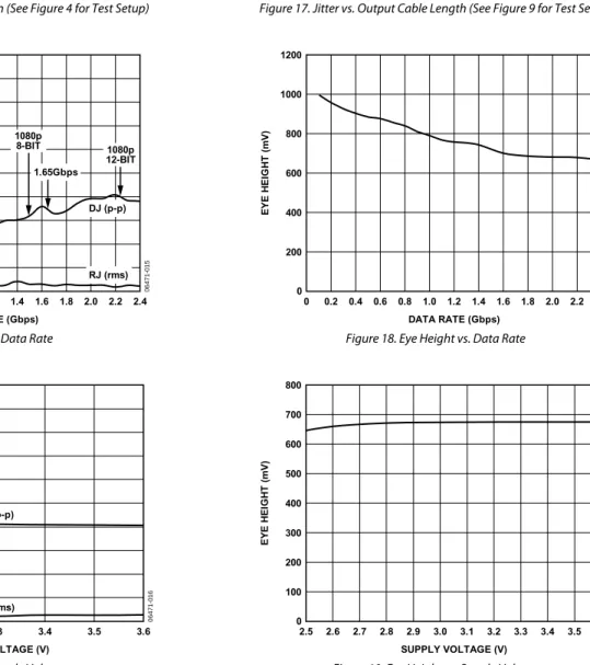
Figure 14. Jitter vs. Input Cable Length (See Figure 4 for Test Setup)
50
0
0 2.4
DATA RATE (Gbps)
JI T T E R ( p s) 45 40 35 30 25 20 15 10 5
0.2 0.4 0.6 0.8 1.0 1.2 1.4 1.6 1.8 2.0 2.2 1080p 12-BIT 1.65Gbps 1080p 8-BIT 1080i/720p 480i 480p DJ (p-p) RJ (rms) 06 471 -01 5
Figure 15. Jitter vs. Data Rate
50
0
3.0 3.6
SUPPLY VOLTAGE (V)
JI T T E R ( p s) 45 40 35 30 25 20 15 10 5
3.1 3.2 3.3 3.4 3.5 RJ (rms) DJ (p-p) 06 47 1-0 1 6
Figure 16. Jitter vs. Supply Voltage
0.5 0.6
0
0 20
HDMI CABLE LENGTH (m)
D E TE R M IN IS T IC J ITT E R ( U I) 0.4 0.3 0.2 0.1
2m CABLE = 30AWG 5m TO 20m CABLES = 24AWG
5 10 15
1.65Gbps, PE MAX 2.25Gbps, PE MAX 1.65Gbps, PE OFF
2.25Gbps, PE OFF
06 471 -01 7 1200 0 0
DATA RATE (Gbps)
EY E H E IG H T ( m V )
Figure 17. Jitter vs. Output Cable Length (See Figure 9 for Test Setup)
1000 800 600 400 200 2.4 06 471 -01 8
0.2 0.4 0.6 0.8 1.0 1.2 1.4 1.6 1.8 2.0 2.2
Figure 18. Eye Height vs. Data Rate
800
0
2.5 3.6
SUPPLY VOLTAGE (V)
EY E H E IG H T ( m V ) 700 600 500 400 300 200 100
2.6 2.7 2.8 2.9 3.0 3.1 3.2 3.3 3.4 3.5
06 47 1-0 1 9
DIFFERENTIAL INPUT SWING (V) JI T T E R ( p s)
TA = 27°C, AVCC = 3.3 V, VTTI = 3.3 V, VTTO = 3.3 V, DVCC = 3.3 V, AMUXVCC = 5 V, AVEE = 0 V, DVEE = 0 V, differential input
swing = 1000 mV, TMDS outputs terminated with external 50 Ω resistors to 3.3 V, pattern = PRBS 27 − 1, data rate = 2.25 Gbps, unless
otherwise noted. 0 0 2.0 40 50 30 20 10 50 0 2.5 3.7
INPUT COMMON-MODE VOLTAGE (V)
JI T T E R ( p s)
0.2 0.4 0.6 0.8 1.0 1.2 1.4 1.6 1.8 RJ (rms) DJ (p-p) 06 47 1-0 2 0
Figure 20. Jitter vs. Differential Input Swing
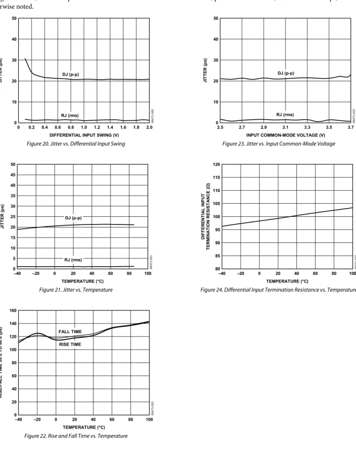
50 0 –40 100 TEMPERATURE (°C) JI T T E R ( p s) 45 40 35 30 25 20 15 10 5
–20 0 20 40 60 80
DJ (p-p) RJ (rms) 06 471 -02 1
Figure 21. Jitter vs. Temperature
160 0 –40 100 TEMPERATURE (°C) RI S E /F A L L T IM E 20% T O 80% ( p s) 140 120 100 80 60 40 20
–20 0 20 40 60 80
RISE TIME FALL TIME 06 47 1-0 2 2
Figure 22. Rise and Fall Time vs. Temperature
40
30
20
10
DJ (p-p)
2.7 2.9 3.1 3.3 3.5 RJ (rms) 06 47 1-0 2 3
Figure 23. Jitter vs. Input Common-Mode Voltage
120 80 –40 100 TEMPERATURE (°C) D IF F E RE NT IA L I NP U T T E RM INAT IO N RE S IS T ANCE ( Ω ) 115 110 105 100 95 90 85
–20 0 20 40 60 80
06
471
-02
4
THEORY OF OPERATION
INTRODUCTION
The AD8197 is a pin-to-pin HDMI 1.3 receive-compliant replacement for the AD8191. The primary function of the AD8197 is to switch one of four (HDMI or DVI) single-link sources to one output. Each HDMI/DVI link consists of four differential, high speed channels and four auxiliary single-ended, low speed control signals. The high speed channels include a data-word clock and three transition minimized differential signaling (TMDS) data channels running at 10× the data-word clock frequency for data rates up to 2.25 Gbps. The four low speed control signals are 5 V tolerant bidirectional lines that can carry configuration signals, HDCP encryption, and other information, depending upon the specific
application.
All four high speed TMDS channels in a given link are identical; that is, the pixel clock can be run on any of the four TMDS channels. Transmit and receive channel compensation is provided for the high speed channels where the user can (manually) select among a number of fixed settings. The AD8197 switching logic has three modes: quad mode (a quad 4:1 switch), dual mode (a dual 8:1 switch), and single mode (one 16:1 switch).
The AD8197 has two control interfaces. Users have the option of controlling the part through either the parallel control interface or the I2C serial control interface. The AD8197 has
eight user-programmable I2C slave addresses to allow multiple
AD8197s to be controlled by a single I2C bus. A RESET pin is
provided to restore the control registers of the AD8197 to default values. In all cases, serial programming values override any prior parallel programming values and any use of the serial control interface disables the parallel control interface until the AD8197 is reset.
When using the serial control interface, all three switching modes (quad, dual, and single) are accessible and the high speed channel switching mode is controlled independently of the auxiliary signal switching mode. When using the parallel control interface, only the quad switching mode is accessible, and the same channel select bus (PP_CH[1:0]) simultaneously switches both the high speed channels and the auxiliary signals.
INPUT CHANNELS
Each high speed input differential pair terminates to the 3.3 V VTTI power supply through a pair of single-ended 50 Ω on-chip resistors, as shown in Figure 25. The input terminations can be optionally disconnected for approximately 100 ms following a source switch. The user can program which of the 16 high speed input channels employs this feature by selectively programming the associated RX_PT bits in the input termination pulse register through the serial control interface. Additionally, all the input terminations can be disconnected by programming the RX_TO bit in the receiver settings register. By default, the
input termination is enabled. The input terminations are enabled and cannot be switched when programming the AD8197 through the parallel control interface.
CABLE EQ 50Ω
50Ω
IP_xx IN_xx
AVEE VTTI
0
64
71
-0
35
Figure 25. High Speed Input Simplified Schematic
The input equalizer can be manually configured to provide two different levels of high frequency boost: 6 dB or 12 dB. The user can individually control the equalization level of the eight high speed input channels by selectively programming the associated RX_EQ bits in the receive equalizer register through the serial control interface. Alternately, the user can globally control the equalization level of all eight high speed input channels by setting the PP_EQ pin of the parallel control interface. No specific cable length is suggested for a particular equalization setting because cable performance varies widely between manufacturers; however, in general, the equalization of the AD8197 can be set to 12 dB without degrading the signal integrity, even for short input cables. At the 12 dB setting, the AD8197 can equalize more than 20 meters of 24 AWG cable at 2.25 Gbps.
OUTPUT CHANNELS
Each high speed output differential pair is terminated to the 3.3 V VTTO power supply through two 50 Ω on-chip resistors (see Figure 26). This termination is user-selectable; it can be turned on or off by programming the TX_PTO bit of the transmitter settings register through the serial control interface, or by setting the PP_OTO pin of the parallel control interface. The output termination resistors of the AD8197 back-terminate the output TMDS transmission lines. These back-terminations, as recommended in the HDMI 1.3 specification, act to absorb reflections from impedance discontinuities on the output traces, improving the signal integrity of the output traces and adding flexibility to how the output traces can be routed. For example, interlayer vias can be used to route the AD8197 TMDS outputs on multiple layers of the PCB without severely degrading the quality of the output signal.
The AD8197 output has a disable feature that places the outputs in a tristate mode. This mode is enabled by programming the HS_EN bit of the high speed device modes register through the serial control interface or by setting the PP_EN pin of the parallel control interface. Larger wire-OR’ed arrays can be constructed using the AD8197 in this mode.
VTTO
50Ω
50Ω
OPx ONx
AVEE DISABLE I
OUT
0
64
71-02
5
Figure 26. High Speed Output Simplified Schematic
The AD8197 requires output termination resistors when the high speed outputs are enabled. Termination can be internal and/or external. The internal terminations of the AD8197 are enabled by programming the TX_PTO bit of the transmitter settings register or by setting the PP_OTO pin of the parallel control interface. The internal terminations of the AD8197 default to the setting indicated by PP_OTO upon reset. External terminations can be provided either by on-board resistors or by the input termination resistors of an HDMI/DVI receiver. If both the internal terminations are enabled and external termi-nations are present, set the output current level to 20 mA by programming the TX_OCL bit of the transmitter settings register through the serial control interface or by setting the PP_OCL pin of the parallel control interface. The output current level defaults to the level indicated by PP_OCL upon reset. If only external terminations are provided (if the internal terminations are disabled), set the output current level to 10 mA by programming the TX_OCL bit of the transmitter settings register or by setting the PP_OCL pin of the parallel control interface. The high speed outputs must be disabled if there are no output termination resistors present in the system.
The output pre-emphasis can be manually configured to provide one of four different levels of high frequency boost. The specific boost level is selected by programming the TX_PE bits of the transmitter settings register through the serial control interface, or by setting the PP_PE bus of the parallel control interface. No specific cable length is suggested for a particular pre-emphasis setting because cable performance varies widely between manufacturers.
HIGH SPEED (TMDS) SWITCHING MODES
The AD8197 has three high speed switching modes: quad, dual, and single. These are selected by programming the HS_SM bits of the high speed device modes register through the serial control interface.
Quad Switching Mode
This is the default mode. In quad mode, the AD8197 behaves like a 4:1 HDMI/DVI link multiplexer routing groups of four TMDS input channels to the four-channel output. This mode is accessible through both the serial and the parallel control interfaces. When using the serial control interface, select which TMDS link is routed to the output by programming the HS_CH bits of the high speed device modes register in accordance with the switch mapping listed in Table 8. When using the parallel
control interface, select which TMDS link is routed to the output by setting the PP_CH bus of the parallel control interface in accordance with the switch mapping listed in Table 26.
Dual Switching Mode
In this mode, the AD8197 behaves as a locked dual [8:1] TMDS channel switch. The two 8:1 switches share the channel select input and, therefore, switch together. Select which two out of the eight possible input groups are routed to output by program-ming the HS_CH bits of the high speed device modes register in accordance with the switch mapping listed in Table 9. This mode is only accessible through the serial control interface.
Single Switching Mode
In this mode, the AD8197 behaves as a single 16:1 TMDS channel multiplexer; one of the 16 input channels is routed to all of the outputs. Select which input channel is routed to the outputs by programming the HS_CH bits in the high speed device modes register in accordance with the switch mapping listed in Table 10. This mode is only accessible through the serial control interface.
AUXILIARY SWITCH
The auxiliary (low speed) lines have no amplification. They are routed using a passive switch that is bandwidth compatible with standard speed I2C. The schematic equivalent for this passive
connection is shown in Figure 27.
AUX_COM0 AUX_A0
½CAUX ½CAUX
RAUX
06
471-02
6
Figure 27. Auxiliary Channel Simplified Schematic, AUX_A0 to AUX_COM0 Routing Example
When turning off the AD8197, care needs to be taken with the AMUXVCC supply to ensure that the auxiliary multiplexer pins remain in a high impedance state. A scenario that illustrates this requirement is one where the auxiliary multiplexer is used to switch the display data channel (DDC) bus. In some applica-tions, additional devices can be connected to the DDC bus (such as an EEPROM with EDID information) upstream of the AD8197. Extended display identification data (EDID) is a VESA standard-defined data format for conveying display configuration information to sources to optimize display use. EDID devices may need to be available via the DDC bus, regardless of the state of the AD8197 and any downstream circuit. For this configuration, the auxiliary inputs of the powered down AD8197 need to be in a high impedance state to avoid pulling down on the DDC lines and preventing these other devices from using the bus.
When the AD8197 is powered from a simple resistor network, as shown in Figure 28, it uses the 5 V supply that is required from any HDMI/DVI source to guarantee high impedance of the auxiliary multiplexer pins. The AMUXVCC supply does not draw any static current; therefore, it is recommended that the resistor network tap the 5 V supplies as close to the connectors as possible to avoid any additional voltage drop.
This precaution does not need to be taken if the DDC peripheral circuitry is connected to the bus downstream of the AD8197.
PERIPHERAL CIRCUITRY PERIPHERAL
CIRCUITRY
+5V SOURCE C
+5V SOURCE D PIN 18 HDMI CONNECTOR
PIN 14 DVI CONNECTOR
PIN 18 HDMI CONNECTOR PIN 14 DVI CONNECTOR
10kΩ
10MΩ
10kΩ
|<50mA
|<50mA PERIPHERAL
CIRCUITRY PERIPHERAL
CIRCUITRY SOURCE A +5V
SOURCE B +5V
PIN 18 HDMI CONNECTOR PIN 14 DVI CONNECTOR
PIN 18 HDMI CONNECTOR PIN 14 DVI CONNECTOR
10kΩ
10kΩ
|<50mA
|<50mA
AMUXVCC AD8197 +5V INTERNAL
(IF ANY)
0
64
71
-00
7
Figure 28. Suggested AMUXVCC Power Scheme
AUXILIARY (LOW SPEED) SWITCHING MODES
The AD8197 has three auxiliary switching modes: quad, dual, and single. These are selected by programming the AUX_SM bits of the auxiliary device modes register through the serial control interface. The auxiliary switching mode is independent of the high speed switching mode whenever the part is controlled through the serial control interface. When the part is controlled through the parallel control interface, however, only quad mode is accessible and the auxiliary switching mode cannot be independently controlled.
Quad Switching Mode
This is the default mode. In quad mode, the AD8197 behaves like a 4:1 auxiliary link multiplexer, routing groups of four auxiliary input signals to the four-signal output. Select which group of inputs is routed to the output by programming the AUX_CH bits of the auxiliary device modes register through the serial control interface in accordance with the switch mapping listed in Table 13. Alternately, select which group of inputs is routed to the output by setting the PP_CH bus of the parallel control interface in accordance with the switch mapping listed in Table 27.
Dual Switching Mode
In this mode, the AD8197 behaves as a locked dual [8:1] auxiliary signal switch. The two 8:1 switches share the channel select input and, therefore, switch together. Select which two out of the eight possible input groups are routed to the output by programming the AUX_CH bits of the auxiliary device modes register in accordance with the switch mapping listed in Table 14. This mode is only accessible through the serial control interface.
Single Switching Mode
In this mode the AD8197 behaves as a single 16:1 TMDS channel multiplexer; a single channel, out of a possible 16, is routed to all of the outputs. Select which input channel is routed to the outputs by programming the AUX_CH bits of the auxiliary device modes register in accordance with the switch mapping listed in Table 15. This mode is only accessible through the serial control interface.
SERIAL CONTROL INTERFACE
RESET
On initial power-up, or at any point in operation, the AD8197 register set can be restored to preprogrammed default values by pulling the RESET pin to low in accordance with the specifica-tions in Table 1. During normal operation, however, the RESET pin must be pulled up to 3.3 V. Following a reset, the prepro-grammed default values of the AD8197 register set correspond to the state of the parallel interface configuration registers, as listed in Table 24. The AD8197 can be controlled through the parallel control interface until the first serial control event occurs. As soon as any serial control event occurs, the serial programming values, corresponding to the state of the serial interface configuration registers (Table 5), override any prior parallel programming values, and the parallel control interface is disabled until the part is subsequently reset.
WRITE PROCEDURE
To write data to the AD8197 register set, an I2C master (such as
a microcontroller) needs to send the appropriate control signals to the AD8197 slave device. The signals are controlled by the I2C master, unless otherwise specified. For a diagram of the
procedure, see Figure 29. The steps for a write procedure are as follows:
1. Send a start condition (while holding the I2C_SCL line high, pull the I2C_SDA line low).
2. Send the AD8197 part address (seven bits). The upper four bits of the AD8197 part address are the static value [1001] and the three LSBs are set by Input Pin I2C_ADDR2, Input Pin I2C_ADDR1, and Input Pin I2C_ADDR0 (LSB). This transfer should be MSB first.
3. Send the write indicator bit (0).
4. Wait for the AD8197 to acknowledge the request. 5. Send the register address (eight bits) to which data is to be
written. This transfer should be MSB first. 6. Wait for the AD8197 to acknowledge the request. 7. Send the data (eight bits) to be written to the register
whose address was set in Step 5. This transfer should be MSB first.
8. Wait for the AD8197 to acknowledge the request. 9. Perform one of the following:
9a. Send a stop condition (while holding the I2C_SCL line high, pull the I2C_SDA line high) and release control of the bus to end the transaction (shown in Figure 29).
9b. Send a repeated start condition (while holding the I2C_SCL line high, pull the I2C_SDA line low) and continue with Step 2 in this procedure to perform another write.
9c. Send a repeated start condition (while holding the I2C_SCL line high, pull the I2C_SDA line low) and continue with Step 2 of the read procedure (in the Read Procedure section) to perform a read from another address.
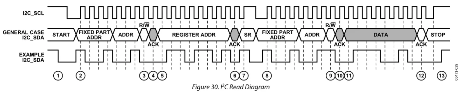
9d. Send a repeated start condition (while holding the I2C_SCL line high, pull the I2C_SDA line low) and continue with Step 8 of the read procedure (in the Read Procedure section) to perform a read from the same address set in Step 5.
R/W
ACK ACK
ADDR
START FIXED PARTADDR REGISTER ADDR DATA STOP
ACK
1 2 3 4 5 6 7 8 9
I2C_SCL
GENERAL CASE I2C_SDA
EXAMPLE I2C_SDA
*THE SWITCHING/UPDATE DELAY BEGINS AT THE FALLING EDGE OF THE LAST DATA BIT; FOR EXAMPLE, THE FALLING EDGE JUST BEFORE STEP 8.
*
0
64
71
-0
28
START FIXED PARTADDR REGISTER ADDR FIXED PARTADDR DATA STOP ACK
ADDR ACK R/W
ADDR
ACK ACK
R/W SR
1 2 3 4 5 6 7 8 9 10 11 12 13
I2C_SCL
GENERAL CASE I2C_SDA
EXAMPLE I2C_SDA
06
47
1-02
9
Figure 30. I2C Read Diagram
READ PROCEDURE
To read data from the AD8197 register set, an I2C master (such
as a microcontroller) needs to send the appropriate control signals to the AD8197 slave device. The signals are controlled by the I2C master, unless otherwise specified. For a diagram of
the procedure, see Figure 30. The steps for a read procedure are as follows:
1. Send a start condition (while holding the I2C_SCL line high, pull the I2C_SDA line low).
2. Send the AD8197 part address (seven bits). The upper four bits of the AD8197 part address are the static value [1001] and the three LSBs are set by Input Pin I2C_ADDR2, Input Pin I2C_ADDR1, and Input Pin I2C_ADDR0 (LSB). This transfer should be MSB first.
3. Send the write indicator bit (0).
4. Wait for the AD8197 to acknowledge the request. 5. Send the register address (eight bits) from which data is to
be read. This transfer should be MSB first. 6. Wait for the AD8197 to acknowledge the request. 7. Send a repeated start condition (Sr) by holding the
I2C_SCL line high and pulling the I2C_SDA line low. 8. Resend the AD8197 part address (seven bits) from Step 2.
The upper four bits of the AD8197 part address are the static value [1001] and the three LSBs are set by the Input Pin I2C_ADDR2, I2C_ADDR1 and Input Pin I2C_ADDR0 (LSB). This transfer should be MSB first.
9. Send the read indicator bit (1).
10. Wait for the AD8197 to acknowledge the request. 11. The AD8197 serially transfers the data (eight bits) held in
the register indicated by the address set in Step 5. This data is sent MSB first.
12. Acknowledge the data from the AD8197.
13. Perform one of the following:
13a.S op condition (while holding the I2C_SCL line high, pull the SDA line high) and release control of the bus to end the transaction (shown in
end a st
). 13b. ted start condition (while holding the
13c.
13d. on (while holding the
SWITCH
writes to the
configura-e
tion
e ly
w;
y Figure 30 Send a repea
I2C_SCL line high, pull the I2C_SDA line low) and continue with Step 2 of the write procedure (previous Write Procedure section) to perform a write. Send a repeated start condition (while holding the I2C_SCL line high, pull the I2C_SDA line low) and continue with Step 2 of this procedure to perform a read from another address.
Send a repeated start conditi
I2C_SCL line high, pull the I2C_SDA line low) and continue with Step 8 of this procedure to perform a read from the same address.
ING/UPDATE DELAY
There is a delay between when a user
tion registers of the AD8197 and when that state change takes physical effect. This update delay occurs regardless of whether the user programs the AD8197 via the serial or the parallel control interface. When using the serial control interface, th update delay begins at the falling edge of I2C_SCL for the last data bit transferred, as shown in Figure 29. When using the parallel control interface, the update delay begins at the transi edge of the relevant parallel interface pin. This update delay is register specific and the times are specified in Table 1. During a delay window, new values can be written to th configuration registers, but the AD8197 does not physical update until the end of that register’s delay window. Writing new values during the delay window does not reset the windo new values supersede the previously written values. At the end of the delay window, the AD8197 physically assumes the state indicated by the last set of values written to the configuration registers. If the configuration registers are written after the dela window ends, the AD8197 immediately updates and a new delay window begins.
PARALLEL CONTROL INTERFACE
The AD8197 can be controlled through the parallel interface using the PP_EN, PP_CH[1:0], PP_EQ, PP_PRE[1:0], PP_OTO, and PP_OCL pins. Logic levels for the parallel interface pins are set in accordance with the specifications listed in Table 1. Setting these pins updates the parallel control interface registers, as listed in Table 24. Following a reset, the AD8197 can be controlled through the parallel control interface until the first serial control event occurs. As soon as any serial control
event occurs, the serial programming values override any prior parallel programming values, and the parallel control interface is disabled until the part is subsequently reset. The default serial programming values correspond to the state of the serial interface configuration registers, as listed in Table 5.
SERIAL INTERFACE CONFIGURATION REGISTERS
The serial interface configuration registers can be read and written using the I2C serial control interface, Pin I2C_SDA, and Pin I2C_SCL.
The least significant bits of the AD8197 I2C part address are set by tying the Pin I2C_ADDR2, Pin I2C_ADDR1, and Pin I2C_ADDR0 to
3.3 V (Logic 1) or 0 V (Logic 0). As soon as the serial control interface is used, the parallel control interface is disabled until the AD8197 is reset as described in the Serial Control Interface section.
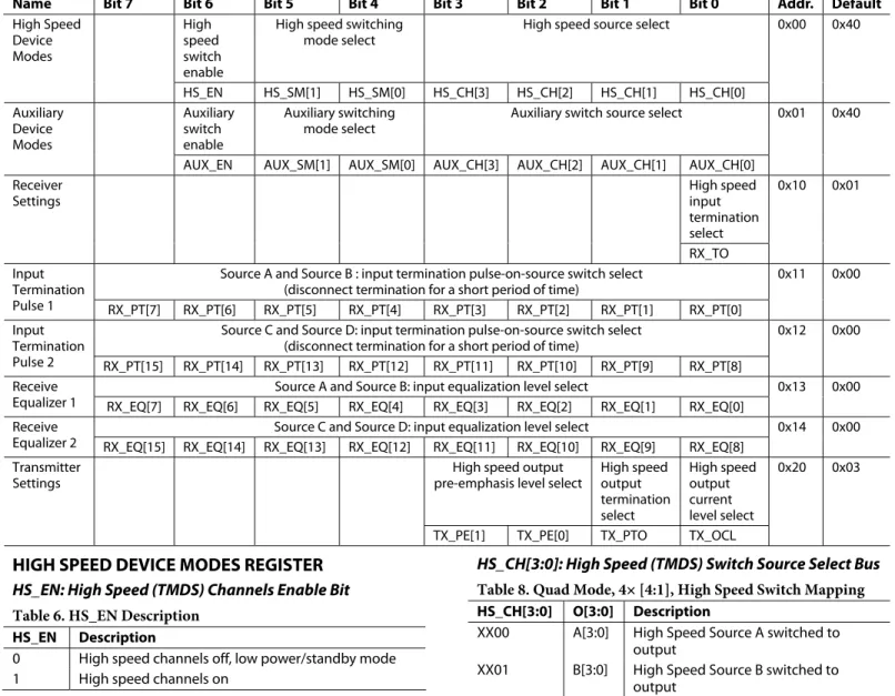
Table 5. Serial (I2C) Interface Register Map
Name Bit 7 Bit 6 Bit 5 Bit 4 Bit 3 Bit 2 Bit 1 Bit 0 Addr. Default
High speed switch enable
High speed switching mode select
High speed source select High Speed
Device Modes
HS_EN HS_SM[1] HS_SM[0] HS_CH[3] HS_CH[2] HS_CH[1] HS_CH[0]
0x00 0x40
Auxiliary switch enable
Auxiliary switching mode select
Auxiliary switch source select Auxiliary
Device Modes
AUX_EN AUX_SM[1] AUX_SM[0] AUX_CH[3] AUX_CH[2] AUX_CH[1] AUX_CH[0]
0x01 0x40
High speed input termination select Receiver
Settings
RX_TO
0x10 0x01
Source A and Source B : input termination pulse-on-source switch select (disconnect termination for a short period of time)
Input Termination
Pulse 1 RX_PT[7] RX_PT[6] RX_PT[5] RX_PT[4] RX_PT[3] RX_PT[2] RX_PT[1] RX_PT[0]
0x11 0x00
Source C and Source D: input termination pulse-on-source switch select (disconnect termination for a short period of time)
Input Termination
Pulse 2 RX_PT[15] RX_PT[14] RX_PT[13] RX_PT[12] RX_PT[11] RX_PT[10] RX_PT[9] RX_PT[8]
0x12 0x00
Source A and Source B: input equalization level select Receive
Equalizer 1 RX_EQ[7] RX_EQ[6] RX_EQ[5] RX_EQ[4] RX_EQ[3] RX_EQ[2] RX_EQ[1] RX_EQ[0]
0x13 0x00 Source C and Source D: input equalization level select
Receive
Equalizer 2 RX_EQ[15] RX_EQ[14] RX_EQ[13] RX_EQ[12] RX_EQ[11] RX_EQ[10] RX_EQ[9] RX_EQ[8]
0x14 0x00 High speed output
pre-emphasis level select
High speed output termination select
High speed output current level select Transmitter
Settings
TX_PE[1] TX_PE[0] TX_PTO TX_OCL
0x20 0x03
HIGH SPEED DEVICE MODES REGISTER
HS_EN: High Speed (TMDS) Channels Enable Bit
Table 6. HS_EN Description
HS_EN Description
0 High speed channels off, low power/standby mode
1 High speed channels on
HS_SM[1:0]: High Speed (TMDS) Switching Mode Select Bus
Table 7. HS_SM Description
HS_SM[1:0] Description
00 Quad mode, 4× [4:1]
01 Dual mode, 2× [8:1]
10 Single mode, 1× [16:1]
11 Illegal value; previous value of HS_SM[1:0]
retained
HS_CH[3:0]: High Speed (TMDS) Switch Source Select Bus
Table 8. Quad Mode, 4× [4:1], High Speed Switch Mapping
HS_CH[3:0] O[3:0] Description
XX00 A[3:0] High Speed Source A switched to
output
XX01 B[3:0] High Speed Source B switched to
output
XX10 C[3:0] High Speed Source C switched to
output
XX11 D[3:0] High Speed Source D switched to
Table 9. Dual Mode, 2× [8:1], High Speed Switch Mapping
HS_CH[3:0] O[3:2] O[1:0] Description
X000 A1 A0 The A0 and A1 high speed
channels switched to output
X001 A3 A2 The A2 and A3 high speed
channels switched to output
X010 B1 B0 The B0 and B1 high speed
channels switched to output
X011 B3 B2 The B2 and B3 high speed
channels switched to output
X100 C1 C0 The C0 and C1 high speed
channels switched to output
X101 C3 C2 The C2 and C3 high speed
channels switched to output
X110 D1 D0 The D0 and D1 high speed
channels switched to output
X111 D3 D2 The D2 and D3 high speed
channels switched to output
Table 10. Single Mode, 1× [16:1], High Speed Switch Mapping
HS_CH[3:0] O[3:0] Description
0000 A0 High Speed Channel A0 switched to
output
0001 A1 High Speed Channel A1 switched to
output
0010 A2 High Speed Channel A2 switched to
output
0011 A3 High Speed Channel A3 switched to
output
0100 B0 High Speed Channel B0 switched to
output
0101 B1 High Speed Channel B1 switched to
output
0110 B2 High Speed Channel B2 switched to
output
0111 B3 High Speed Channel B3 switched to
output
1000 C0 High Speed Channel C0 switched to
output
1001 C1 High Speed Channel C1 switched to
output
1010 C2 High Speed Channel C2 switched to
output
1011 C3 High Speed Channel C3 switched to
output
1100 D0 High Speed Channel D0 switched to
output
1101 D1 High Speed Channel D1 switched to
output
1110 D2 High Speed Channel D2 switched to
output
1111 D3 High Speed Channel D3 switched to
output
AUXILIARY DEVICE MODES REGISTER
AUX_EN: Auxiliary (Low Speed) Switch Enable Bit
Table 11. AUX_EN Description
AUX_EN Description
0 Auxiliary switch off, no low speed input/output
to low speed common input/output connection
1 Auxiliary switch on
AUX_SM[1:0]: Auxiliary (Low Speed) Switching Mode Select Bus
Table 12. AUX_SM[1:0] Description
AUX_SM[1:0] Description
00 Quad Mode, 4× [4:1]
01 Dual Mode, 2× [8:1]
10 Single Mode, 1× [6:1]
11 Illegal value; previous value of AUX_SM[1:0]
retained
AUX_CH[3:0]: Auxiliary (Low Speed) Switch Source Select Bus
Table 13. Quad Mode, 4× [4:1], Auxiliary Switch Mapping
AUX_CH[3:0] AUX_COM[3:0] Description
XX00 AUX_A[3:0] Auxiliary Source A switched
to output
XX01 AUX_B[3:0] Auxiliary Source B switched
to output
XX10 AUX_C[3:0] Auxiliary Source C switched
to output
XX11 AUX_D[3:0] Auxiliary Source D switched
Table 14. Dual Mode, 2× [8:1], Auxiliary Switch Mapping
AUX_CH[3:0] AUX_COM[3:2] AUX_COM[1:0] Description
X000 AUX_C0 AUX_A0 The A0 and
C0 auxiliary channels switched to output
X001 AUX_C1 AUX_A1 The A1 and
C1 auxiliary channels switched to output
X010 AUX_C2 AUX_A2 The A2 and
C2 auxiliary channels switched to output
X011 AUX_C3 AUX_A3 The A3 and
C3 auxiliary channels switched to output
X100 AUX_D0 AUX_B0 The B0 and
D0 auxiliary channels switched to output
X101 AUX_D1 AUX_B1 The B1 and
D1 auxiliary channels switched to output
X110 AUX_D2 AUX_B2 The B2 and
D2 auxiliary channels switched to output
X111 AUX_D3 AUX_B3 The B3 and
D3 auxiliary channels switched to output
Table 15. Single Mode, 1× [16:1], Auxiliary Switch Mapping
AUX_CH[3:0] AUX_COM[3:0] Description
0000 AUX_A0 Auxiliary Channel A0
switched to output
0001 AUX_A1 Auxiliary Channel A1
switched to output
0010 AUX_A2 Auxiliary Channel A2
switched to output
0011 AUX_A3 Auxiliary Channel A3
switched to output 0100 AUX_B0 Auxiliary Channel B0
switched to output 0101 AUX_B1 Auxiliary Channel B1
switched to output 0110 AUX_B2 Auxiliary Channel B2
switched to output 0111 AUX_B3 Auxiliary Channel B3
switched to output
1000 AUX_C0 Auxiliary Channel C0
switched to output
1001 AUX_C1 Auxiliary Channel C1
switched to output
1010 AUX_C2 Auxiliary Channel C2
switched to output
1011 AUX_C3 Auxiliary Channel C3
switched to output
1100 AUX_D0 Auxiliary Channel D0
switched to output
1101 AUX_D1 Auxiliary Channel D1
switched to output
1110 AUX_D2 Auxiliary Channel D2
switched to output
1111 AUX_D3 Auxiliary Channel D3
RECEIVER SETTINGS REGISTER
RX_TO: High Speed (TMDS) Channels Input Termination On/Off Select Bit
Table 16. RX_TO Description
RX_TO Description
0 Input termination off
1 Input termination on (can be pulsed on and off
according to settings in the input termination pulse register)
INPUT TERMINATION PULSE REGISTER 1 AND
REGISTER 2
RX_PT[X]: High Speed (TMDS) Input Channel X Pulse-On-Source Switch Select Bit
Table 17. RX_PT[X] Description
RX_PT[X] Description
0 Input termination for TMDS Channel X always
connected when source is switched
1 Input termination for TMDS Channel X
disconnected for 100 ms when source switched
Table 18. RX_PT[X] Mapping
RX_PT[X] Corresponding Input TMDS Channel
Bit 0 B0
Bit 1 B1
Bit 2 B2
Bit 3 B3
Bit 4 A0
Bit 5 A1
Bit 6 A2
Bit 7 A3
Bit 8 C3
Bit 9 C2
Bit 10 C1
Bit 11 C0
Bit 12 D3
Bit 13 D2
Bit 14 D1
Bit 15 D0
RECEIVE EQUALIZER REGISTER 1 AND REGISTER 2
RX_EQ[X]: High Speed (TMDS) Input X Equalization Level Select Bit
Table 19. RX_EQ[X] Description
RX_EQ[X] Description
0 Low equalization (6 dB)
1 High equalization (12 dB)
Table 20. RX_EQ[X] Mapping
RX_EQ[X] Corresponding Input TMDS Channel
Bit 0 B0
Bit 1 B1
Bit 2 B2
Bit 3 B3
Bit 4 A0
Bit 5 A1
Bit 6 A2
Bit 7 A3
Bit 8 C3
Bit 9 C2
Bit 10 C1
Bit 11 C0
Bit 12 D3
Bit 13 D2
Bit 14 D1
Bit 15 D0
TRANSMITTER SETTINGS REGISTER
TX_PE[1:0]: High Speed (TMDS) Output Pre-Emphasis Level Select Bus (For All TMDS Channels)
Table 21. TX_PE[1:0] Description
TX_PE[1:0] Description
00 No pre-emphasis (0 dB)
01 Low pre-emphasis (2 dB)
10 Medium pre-emphasis (4 dB)
11 High pre-emphasis (6 dB)
TX_PTO: High Speed (TMDS) Output Termination On/Off Select Bit (For All Channels)
Table 22. TX_PTO Description
TX_PTO Description
0 Output termination off
1 Output termination on
TX_OCL: High Speed (TMDS) Output Current Level Select Bit (For All Channels)
Table 23. TX_OCL Description
TX_OCL Description
0 Output current set to 10 mA
PARALLEL INTERFACE CONFIGURATION REGISTERS
The parallel interface configuration registers can be directly set using the PP_EN, PP_CH[1:0], PP_EQ, PP_PRE[1:0], PP_OTO, and PP_OCL pins. This interface is only accessible after the part is reset and before any registers are accessed using the serial control interface. The state of each pin is set by tying it to 3.3 V (Logic 1) or 0 V (Logic 0).
Table 24. Parallel Interface Register Map
Name Bit 7 Bit 6 Bit 5 Bit 4 Bit 3 Bit 2 Bit 1 Bit 0
High speed switch enable
High speed switching mode select (quad)
High speed source select High Speed
Device Modes
PP_EN 0 0 0 0 PP_CH[1] PP_CH[0] Auxiliary
switch enable
Auxiliary switching mode select (quad)
Auxiliary switch source select Auxiliary Device
Modes
1 0 0 0 0 PP_CH[1] PP_CH[0]
Input term. on/off select (termination always on) Receiver
Settings
1 Source A and Source B input termination pulse-on-source switch select (termination always on) Input
Termination
Pulse 1 0 0 0 0 0 0 0 0
Source C and Source D input termination pulse-on-source switch select (termination always on) Input
Termination
Pulse 2 0 0 0 0 0 0 0 0
Source A and Source B input equalization level select Receive
Equalizer 1 PP_EQ PP_EQ PP_EQ PP_EQ PP_EQ PP_EQ PP_EQ PP_EQ
Source C and Source D input equalization level select Receive
Equalizer 2 PP_EQ PP_EQ PP_EQ PP_EQ PP_EQ PP_EQ PP_EQ PP_EQ
Output pre-emphasis level select
Output termination on/off select
Output current level select
Transmitter Settings
PP_PE[1] PP_PE[0] PP_OTO PP_OCL
HIGH SPEED DEVICE MODES REGISTER
The high speed (TMDS) switching mode is fixed to quad mode when using the parallel interface.
PP_EN: High Speed (TMDS) Channels Enable Bit
Table 25. PP_EN Description
PP_EN Description
0 High speed channels off, low power/standby mode
1 High speed channels on
PP_CH[1:0]: High Speed (TMDS) Switch Source Select Bus
Table 26. Quad High speed Switch Mode Mapping
PP_CH[1:0] O[3:0] Description
00 A[3:0] High Speed Source A switched to
output
01 B[3:0] High Speed Source B switched to
output
10 C[3:0] High Speed Source C switched to
output
11 D[3:0] High Speed Source D switched to
output
AUXILIARY DEVICE MODES REGISTER
The auxiliary (low speed) switch is always enabled and the auxiliary switching mode is fixed to quad mode when using the parallel interface.
PP_CH[1:0]: Auxiliary Switch Source Select Bus
Table 27. Quad Auxiliary Switch Mode Mapping
PP_CH[1:0] AUX_COM[3:0] Description
00 AUX_A[3:0] Auxiliary Source A switched to
output
01 AUX_B[3:0]0 Auxiliary Source B switched to
output
10 AUX_C[3:0] Auxiliary Source C switched to
output
11 AUX_D[3:0] Auxiliary Source D switched to
RECEIVER SETTINGS REGISTER
High speed (TMDS) channels input termination is fixed to on when using the parallel interface.
INPUT TERMINATION PULSE REGISTER 1 AND
REGISTER 2
High speed input (TMDS) channels pulse-on-source switching fixed to off when using the parallel interface.
RECEIVE EQUALIZER REGISTER 1 AND REGISTER 2
PP_EQ: High Speed (TMDS) Inputs Equalization Level Select Bit (For All TMDS Input Channels)
The input equalization cannot be set individually (per channel) when using the parallel interface; one equalization setting affects all input channels.
Table 28. PP_EQ Description
PP_EQ Description
0 Low equalization (6 dB)
1 High equalization (12 dB)
TRANSMITTER SETTINGS REGISTER
PP_PE[1:0]: High Speed (TMDS) Output Pre-Emphasis Level Select Bus (For All TMDS Channels)
Table 29. PP_PE[1:0] Description
PP_PE[1:0] Description
00 No pre-emphasis (0 dB)
01 Low pre-emphasis (2 dB)
10 Medium pre-emphasis (4 dB)
11 High pre-emphasis (6 dB)
PP_OTO: High Speed (TMDS) Output Termination On/Off Select Bit (For All TMDS Channels)
Table 30. PP_OTO Description
PP_OTO Description
0 Output termination off
1 Output termination on
PP_OCL: High Speed (TMDS) Output Current Level Select Bit (For All TMDS Channels)
Table 31. TX_OCL Description
PP_OCL Description
0 Output current set to 10 mA
APPLICATION INFORMATION
0
64
71
-0
30
Figure 31. Layout of the TMDS Traces on the AD8197 Evaluation Board (Only Top Signal Routing Layer is Shown)
The AD8197 is an HDMI/DVI switch, featuring equalized TMDS inputs and pre-emphasized TMDS outputs. It is in-tended for use as a 4:1 switch in systems with long cable runs on both the input and/or the output, and is fully HDMI 1.3 receive-compliant.
PINOUT
The AD8197 is designed to have an HDMI/DVI receiver pinout at its input and a transmitter pinout at its output. This makes the AD8197 ideal for use in AVR-type applications where a designer routes both the inputs and the outputs directly to HDMI/DVI connectors, as shown in Figure 31. When the AD8197 is used in receiver type applications, it is necessary to change the order of the output pins on the PCB to align with the on-board receiver.
One advantage of the AD8197 in an AVR-type application is that all of the high speed signals can be routed on one side (the topside) of the board, as shown in Figure 31. In addition to 12 dB of input equalization, the AD8197 provides up to 6 dB of output pre-emphasis that boosts the output TMDS signals and allows the AD8197 to precompensate when driving long PCB traces or output cables. The net effect of the input equalization and output pre-emphasis of the AD8197 is that the AD8197 can compensate for the signal degradation of both input and output
cables; it acts to reopen a closed input data eye and transmit a full-swing HDMI signal to an end receiver. More information on the specific performance metrics of the AD8197 can be found in the Typical Performance Characteristics section. The AD8197 also provides a distinct advantage in receive-type applications because it is a fully buffered HDMI/DVI switch. Although inverting the output pin order of the AD8197 on the PCB requires a designer to place vias in the high speed signal path, the AD8197 fully buffers and electrically decouples the outputs from the inputs. Therefore, the effects of the vias placed on the output signal lines are not seen at the input of the AD8197. The programmable output terminations also improve signal quality at the output of the AD8197. The PCB designer, therefore, has significantly improved flexibility in the placement and routing of the output signal path with the AD8197 over other solutions.
CABLE LENGTHS AND EQUALIZATION
The AD8197 offers two levels of programmable equalization for the high speed inputs: 6 dB and 12 dB. The equalizer of the AD8197 supports video data rates of up to 2.25 Gbps, and as shown in Figure 14, it can equalize more than 20 meters of 24 AWG HDMI cable at 2.25 Gbps, which corresponds to the video format, 1080p with deep color.


![Table 9. Dual Mode, 2× [8:1], High Speed Switch Mapping HS_CH[3:0] O[3:2] O[1:0] Description](https://thumb-us.123doks.com/thumbv2/123dok_us/8503881.2275931/21.918.463.850.111.471/table-dual-mode-high-speed-switch-mapping-description.webp)
![Table 14. Dual Mode, 2× [8:1], Auxiliary Switch Mapping AUX_CH[3:0] AUX_COM[3:2] AUX_COM[1:0] Description X000 AUX_C0 AUX_A0 The A0 and](https://thumb-us.123doks.com/thumbv2/123dok_us/8503881.2275931/22.918.201.868.129.786/table-dual-mode-auxiliary-switch-mapping-aux-description.webp)
