Application Report
SLEA106 – July 2010
TVP51471M1 VBI Quick Start
...
ABSTRACT
The TVP5147M1 video decoder has an internal vertical data processor (VDP) that can be used to slice
various VBI data services such as V-Chip, teletext (WST, NABTS), closed captioning (CC), wide screen
signaling (WSS), copy generation management system (CGMS), video program system (VPS), electronic
program guide (EPG or Gemstar), program delivery control (PDC) and vertical interval time code (VITC).
This application report provides an introduction to the VBI data slicing capabilities of the TVP5147M1 and
focuses on configuring the TVP5147M1 for the more commonly used VBI data services.
Contents
1 Introduction
...
22 VBUS Access
...
33 General Line-Mode and Line-Address
...
34 I2C Sliced Data Retrieval
...
45 Managing Data Retrieval
...
56 FIFO Access
...
67 Ancillary Data
...
68 Full-Field Mode
...
79 VBI Raw Data Mode
...
8Appendix A Subset of the TVP5147M1 VDP I2C Registers
...
10Appendix B Sample WinVCC CMD File for VBI Setup
...
18Appendix C VBI Raw Data I2C Registers
...
19List of Figures 1 TVP5147M1 VBUS Write Example
...
32 I2C Read of WSS/CGMS Data Registers at VBUS Address 80 0520h
...
53 Example WSS/CGMS Data Retrieval
...
64 Line 21 Closed Caption ITU-R BT.656 Digital Output Capture with YUV Samples Present.Raw Data Mode is Disabled.
...
95 Line 21 Closed Caption ITU-R BT.656 Digital Output Capture in Raw Data Mode.UV (Chroma) Data are Replaced with Y (Luma) Data.
...
9List of Tables 1 Supported Data Services
...
22 Typical Line-Mode and Line-Address Setup
...
43 Dedicated VDP VBUS Data Registers
...
44 Ancillary Data Header
...
75 525-Line Raw Data Setup to Include Line 21
...
8Introduction www.ti.com
1
Introduction
The TVP5147M1 video decoder has an internal vertical data processor (VDP) that can be used to slice
various VBI data services such as V-Chip, teletext (WST, NABTS), closed captioning (CC), wide screen
signaling (WSS), copy generation management system (CGMS), video program system (VPS), electronic
program guide (EPG or Gemstar), program delivery control (PDC), and vertical interval time code (VITC).
These data services are typically transmitted during the vertical blanking interval of the video frame.
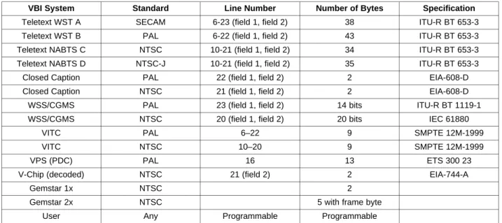
Table 1
provides a summary of the supported data services including the line numbers on which they are
typically transmitted.
Table 1. Supported Data Services
VBI System Standard Line Number Number of Bytes Specification
Teletext WST A SECAM 6-23 (field 1, field 2) 38 ITU-R BT 653-3
Teletext WST B PAL 6-22 (field 1, field 2) 43 ITU-R BT 653-3
Teletext NABTS C NTSC 10-21 (field 1, field 2) 34 ITU-R BT 653-3
Teletext NABTS D NTSC-J 10-21 (field 1, field 2) 35 ITU-R BT 653-3
Closed Caption PAL 22 (field 1, field 2) 2 EIA-608-D
Closed Caption NTSC 21 (field 1, field 2) 2 EIA-608-D
WSS/CGMS PAL 23 (field 1, field 2) 14 bits ITU-R BT 1119-1
WSS/CGMS NTSC 20 (field 1, field 2) 20 bits IEC 61880
VITC PAL 6–22 9 SMPTE 12M-1999
VITC NTSC 10–20 9 SMPTE 12M-1999
VPS (PDC) PAL 16 13 ETS 300 23
V-Chip (decoded) NTSC 21 (field 2) 2 EIA-744-A
Gemstar 1x NTSC 2
Gemstar 2x NTSC 5 with frame byte
User Any Programmable Programmable
A host or backend receiver can retrieve the sliced data using one of three methods:
•
I
2C access of dedicated Closed Caption, WSS, CGMS, VPS, Gemstar, VITC, and V-Chip data
registers.
•
I
2C access of an internal 512-byte FIFO used primarily for high-bandwidth data services such as
full-field teletext.
•
As ITU-R BT.656 ancillary data, inserted by the TVP5147M1 in the data stream during the horizontal
blanking interval.
Note: This document will focus primarily on the more commonly used dedicated I
2C data registers.
The TVP5147M1 provides automatic decode of V-Chip TV rating data used for parental control. In all
other cases, host software must be used to decode the sliced VBI data. Prior to accessing the sliced data,
the TVP5147M1 must be configured for the desired VBI data service. This includes I
2C setup for the
desired data service and the line numbers where they occur within the video frame. This process is fully
programmable through use of the VDP general line-mode registers (VBUS subaddress 80 0600h-80
0611h). As seen in the following sections, some of the I
2C registers related to the VDP setup and data
retrieval can be accessed directly with I
2C, while others must be accessed indirectly through use of the
internal VBUS. Detailed descriptions of the VBI-related I
2// TVP5147M1 VBUS Write Example
#define TVP5147M1 0xB8; // TVP5147M1 main I2C address byte I2C_RegAddress;
int count;
byte I2CData ={0x14,0x02}; // VBUS 24bitAddress = 0x800600;
// write 800605h to VBUS 24bit address registers I2C_RegAddress = 0xE8;
I2CWriteByte(TVP5147M1, I2C_RegAddress, 0x00); // write VBUS address [7:0} to E8h I2C_RegAddress++;
I2CWriteByte(TVP5147M1, I2C_RegAddress, 0x06); // write VBUS address [15:8} to E9h I2C_RegAddress++;
I2CWriteByte(TVP5147M1, I2C_RegAddress, 0x80); // write VBUS address [23:16} to EAh // write 2 data bytes to the VBUS using address auto-increment with register E1h For (count = 0; count < 2; count ++)
{
I2CWriteByte(TVP5147M1, 0xE1, I2C_Data[count]); // write data bytes to E1h }
www.ti.com VBUS Access
2
VBUS Access
Many of the VBI related I
2C registers, including the general line-mode registers and sliced-data registers,
must be accessed over the VBUS interface using the VBUS address access registers (E8h-EAh) and one
of the VBUS data access registers (E0h-E1h). The VBUS address access register contains 3 bytes to
accommodate the 24bit VBUS address bus of the TVP5147M1. After the 24-bit address is loaded, data
reads and writes are performed through one the data access registers, depending on whether address
auto-increment is desired. The example in
Figure 1
writes 2 bytes of data to VBUS address 80 0600h
using the automatic VBUS address-increment register E1h.
Example (Write 2 data bytes to VBUS address 80 0600h and 80 0601h.)
1. Set the VBUS address to 80 0600h.
(a) Write 80h to I
2C address EAh.
(b) Write 06h to I
2C address E9h.
(c) Write 00h to I
2C address E8h.
2. Write the 2 data bytes
(a) Write 14h to I
2C address E1h. (Note that register E1h is the autoincrementing VBUS register. After
writing 15h to this register, the internal VBUS address automatically increments to 80 0601h).
(b) Write 02h to I
2C address E1h.
Figure 1. TVP5147M1 VBUS Write Example
3
General Line-Mode and Line-Address
Prior to accessing sliced VBI data, the general line-mode and line-address registers (80 0600h-80 0611h)
must be properly configured for the desired VBI data service. This bank of 18 registers is grouped in pairs
(line-address and line-mode) providing a total of nine possible entries. The register pairs set up the video
line number, video field, and the VBI data service for that particular line number. Additional data slicing
options such as filtering, error correction, and FIFO routing are also available in the line-mode registers. A
detailed description of these registers is shown in Appendix A.
Table 2
shows a typical setup for several of
the supported data services. Following setup of these registers, sliced VBI data should be available for
retrieval, if present. Unused line-mode and line-address registers must be programmed with FFh.
I2C Sliced Data Retrieval www.ti.com
Table 2. Typical Line-Mode and Line-Address Setup
Subaddress Data Register Description
80 0600h 15h Line-address 1 Line 21
80 0601h 01h Line-mode 1 Closed Caption (field 1)
80 0602h 15h Line-address 2 Line 21
80 0603h 09h Line-mode 2 Closed Caption (field2)
80 0604h 14h Line-address 3 Line 20
80 0605h 02h Line-mode 3 WSS/CGMS (field 1)
80 0606h 0Ah Line-address 4 Line 10
80 0607h 00h Line-mode 4 Teletext (field 1)
80 0608h 0Ah Line-address 5 Line 10
80 0609h 08h Line-mode 5 Teletext (field 2)
80 060Ah FFh Line-address 6 Not used
80 060Bh FFh Line-mode 6 Not used
80 060Ch FFh Line-address 7 Not used
80 060Dh FFh Line-mode 7 Not used
80 060Eh FFh Line-address 8 Not used
80 060Fh FFh Line-mode 8 Not used
80 0610h FFh Line-address 9 Not used
80 0611h FFh Line-mode 9 Not used
4
I
2C Sliced Data Retrieval
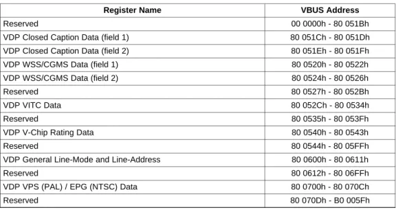
The TVP5147M1 provides dedicated VBUS VDP data registers (
Table 3
) for storage of the sliced data.
Due to higher bandwidth requirements, teletext data is stored in a 512 byte FIFO. With all other data
services, sliced data can be automatically sent to the dedicated registers or to the FIFO depending on the
line-mode setup. The line-mode setup in
Table 2
results in teletext data being routed to the FIFO and all
other sliced data being routed to their dedicated registers. The host access enable bit in I
2C register C0h
must also be set to logic 1 to enable I
2C FIFO access.
Table 3. Dedicated VDP VBUS Data Registers
Register Name VBUS Address
Reserved 00 0000h - 80 051Bh
VDP Closed Caption Data (field 1) 80 051Ch - 80 051Dh
VDP Closed Caption Data (field 2) 80 051Eh - 80 051Fh
VDP WSS/CGMS Data (field 1) 80 0520h - 80 0522h
VDP WSS/CGMS Data (field 2) 80 0524h - 80 0526h
Reserved 80 0527h - 80 052Bh
VDP VITC Data 80 052Ch - 80 0534h
Reserved 80 0535h - 80 053Fh
VDP V-Chip Rating Data 80 0540h - 80 0543h
Reserved 80 0544h - 80 05FFh
VDP General Line-Mode and Line-Address 80 0600h - 80 0611h
Reserved 80 0612h - 80 06FFh
VDP VPS (PAL) / EPG (NTSC) Data 80 0700h - 80 070Ch
// TVP5147M1 VBUS Read of VDP WSS/CGMS Data Registers
#define TVP5147M1 0xB8; // TVP5147M1 main I2C address
int count; byte WSSData[3];
// VDP WSS/CGMS Data Registers VBUS 24bit Address = 0x800520; // write 800520h to VBUS 24bit address registers
I2CWriteByte(TVP5147M1, 0xC0, 0x01); // Set host Enable to 1 to enable FIFO Access // Set to 0 for video port ancillary data byte I2C_RegAddress = 0xE8;
I2CWriteByte(TVP5147M1, I2C_RegAddress, 0x20); // write VBUS address [7:0} to E8h
I2C_RegAddress++;
I2CWriteByte(TVP5147M1, I2C_RegAddress, 0x05); // write VBUS address [15:8} to E9h
I2C_RegAddress++;
I2CWriteByte(TVP5147M1, I2C_RegAddress, 0x80); // write VBUS address [23:16} to EAh
// read 3 data bytes from WSS/CGMS Data Register For (count = 0; count < 3; count ++)
{
WSSData[count]=I2CReadByte(TVP5147M1, 0xE1); // read 3 bytes from E1h
}
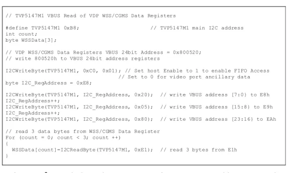
www.ti.com Managing Data Retrieval
Reading the VBUS VDP data registers is very similar to a VBUS write operation, with the only difference
being that data is read from the VBUS data access register.
Figure 2
shows a typical read of sliced
WSS/CGMS data using the address auto-increment method (data access register E1h).
Figure 2. I
2C Read of WSS/CGMS Data Registers at VBUS Address 80 0520h
5
Managing Data Retrieval
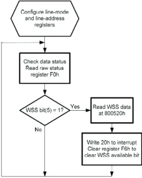
The interrupt raw status registers (F0h-F1h) can be used to determine when sliced data is available.
Unmasked data-available bits for the supported data services are provided in the interrupt raw status 0
register, which is directly accessible at I
2C register F0h.
Interrupt Raw Status 0 Subaddress F0h
7 6 5 4 3 2 1 0
FIFO THRS TTX WSS/CGMS VPS/Gemstar VITC CC F2 CC F1 Line
A logic 1 indicates that sliced data is available. Once set, these bits need to be reset by writing a logic 1 to the appropriate bits in the interrupt clear registers (F6h).Figure 3shows a typical procedure for retrieving WSS/CGMS data.
FIFO Access www.ti.com
Figure 3. Example WSS/CGMS Data Retrieval
6
FIFO Access
The internal 512 byte FIFO is used primarily for high-bandwidth teletext acquisition, but can also be used
for capture of the other data services. The FIFO can be directly accessed by the host at I
2C address E2h.
Bit 0 of the VDP FIFO output control register (C0h) must be set to logic 1 to enable host access to the
FIFO. A header containing information about the sliced data precedes all sliced data that is routed to the
FIFO. A VDP FIFO interrupt threshold register (BDh), FIFO threshold bit, and FIFO full interrupt/status bits
(see F0h–F7h) are available for managing data flow.
7
Ancillary Data
An option is available to enable transmission of sliced VBI data as ancillary data in the ITU-R BT.656
video data stream. In this mode, the sliced data is inserted on the Y[9:2] output terminals during the
horizontal blanking interval. Due to device latency, the ancillary data is inserted one line prior to the digital
line where it occurred. An 8-byte header containing information about the sliced data is also inserted in the
data stream prior to the sliced data. The header includes a 00h, FFh, FFh preamble that identifies the data
as VBI ancillary data, so the host or back end must be able to distinguish between this preamble and the
ITU-R BT.656 embedded sync codes (FFh, 00h, 00h, E/SAV). The first header byte is inserted
immediately following the EAV code. The ancillary data header is summarized in
Table 4
.
The ancillary data mode is enabled by setting bit 6 in the appropriate line-mode register to a logic 1 and
the host-access enable bit (bit 0) in register C0h to a logic 0. To enable ancillary data output for line-7
teletext, for example, 40h is written to the line-7 line-mode register, and 00h is written to register C0h.
When the ancillary data mode is enabled in register C0h, sliced data is not routed to the internal 512-byte
FIFO.
www.ti.com Full-Field Mode
Table 4. Ancillary Data Header
Byte D7 D6 D5 D4 D3 D2 D1 D0 Description
No. (MSB) (LSB)
0 0 0 0 0 0 0 0 0
1 1 1 1 1 1 1 1 1 Ancillary data preamble
2 1 1 1 1 1 1 1
3 NEP EP 0 1 0 DID2 DID1 DID0 Data ID (DID)
4 NEP EP F5 F4 F3 F2 F1 F0 Secondary data ID (SDID)
5 NEP EP N5 N4 N3 N2 N1 N0 Number of 32 bit data (NN)
6 Video line # [7:0] Internal Data ID0 (IDID0)
Data Match Match
7 0 0 0 Video line # [9:8] Internal Data ID1 (IDID1)
error #1 #2
8 1. Data Data byte 1stword
9 2. Data Data byte
10 3. Data Data byte
11 4. Data Data byte
... ... ...
m-1. Data Data byte Nthword
m. Data Data byte
CS [7:0] Checksum
4N + 7 0 0 0 0 0 0 0 0 Fill byte
EP: Even parity for D0–D5 NEP: Negate even parity
DID: 91h: Sliced data from the vertical blanking interval of first field
53h: Sliced data from outside of the vertical blanking interval of first field 55h: Sliced data from the vertical blanking interval of second field
97h: Sliced data from outside of the vertical blanking interval of second field SDID: This field holds the data format taken from the line-mode register of the corresponding line. NN: Number of Dwords beginning with byte 8 through 4N+7. Note that each Dword is 4 bytes. IDID0: Transaction video line number [7:0]
IDID1: Bit 0/1: Transaction video line number [9:8] Bit 2: Match 2 flag
Bit 3: Match 1 flag
Bit 4: Value = 1 if a single error was detected in the EDC block. Value = 0 if no error was detected. CS: Sum of D0–D7 of 1.Data through last data byte.
Fill byte: Fill byte makes a multiple of 4 bytes from byte zero to last fill byte. Note: The number of bytes (m) varies depending on the VBI data service.
8
Full-Field Mode
Some teletext services transmit data on multiple video lines occurring anywhere in the video field. The
TVP5147M1 provides a full-field mode which arms VDP slicing for all lines in the video field. When
full-field mode is enabled, all video lines excluding those defined in the general line-mode registers are
sliced as specified in the VDP full-field mode register (DAh). The full-field Mode register uses the same
mode configuration format as the general line-mode registers. Full-field mode is enabled by setting the
full-field enable bit in register D9h to a logic 1. Sliced data is then retrieved by I
2C FIFO access or as
ancillary data in the ITU-R BT.656 data stream.
VBI Raw Data Mode www.ti.com
9
VBI Raw Data Mode
The TVP5147M1 offers a VBI raw data mode for use in systems where VBI data slicing and processing is
handled in the digital backend receiver instead of the video decoder. In this mode of operation, the
decoders are configured to output raw 2x over-sampled luma data on the ITU-R BT.656 output during the
defined VBLK (vertical blanking) interval. The raw, un-sliced A/D video data is transmitted during the
active video portion of the line with chroma samples being replaced with the luma samples.
The default VBLK interval for Field 1 is defined as lines 1 through 20 for 525-line video formats and lines
623 through 23 for 625-line video formats. This interval may be adjusted to include additional lines.
Support for NTSC line 21 closed caption data, for example, requires extension of the VBLK interval to
include line 21.
The TVP5147M1 default vertical blanking interval for Field 1 is defined as lines 1 through 20 for 525-line
video formats and lines 623 through 23 for 625-line video formats. This interval is programmable with the
VBLK Start Line and VBLK Stop Line I
2C registers (22h-25h). The VBLK Start and Stop registers in the
TVP5147M1 are programmed with absolute line numbers. After configuring the desire VBLK interval, the
VBI raw bit (bit 4) in the Luminance Processing Control 1 register (06h) must be set to a logic 1 to enable
raw data output.
Table 1
shows the default I
2C registers with modified VBLK registers for Line 21
inclusion, while
Table 2
shows the default 625-line setup. Also shown in
Figure 1
and
Figure 2
are digital
captures of the TVP5147M1 ITU-R BT.656 output for comparison of normal operation and raw data
operation. A four-byte preamble (000h 3FFh 3FFh 180h) is inserted by the TVP5147M1 prior to the start of
the raw data.
Note: The TVP5147M1 VBLK start and stop values are absolute line numbers. Other TI video decoders,
such as the TVP5150A, may use values that are relative adjustments to the default VBLK interval.
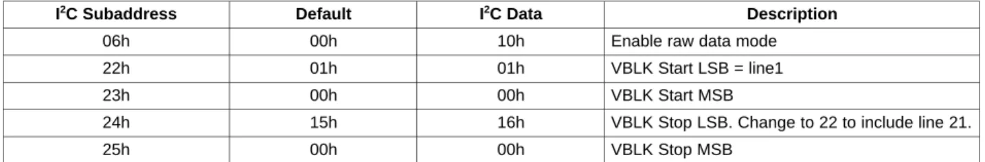
Table 5. 525-Line Raw Data Setup to Include Line 21
I2C Subaddress Default I2C Data Description
06h 00h 10h Enable raw data mode
22h 01h 01h VBLK Start LSB = line1
23h 00h 00h VBLK Start MSB
24h 15h 16h VBLK Stop LSB. Change to 22 to include line 21.
25h 00h 00h VBLK Stop MSB
Table 6. 625-Line Raw Data Setup
I2C Subaddress Default I2C Data Description
06h 00h 10h Enable raw data mode
22h 6Fh 6Fh VBLK Start LSB = line 623 default
23h 02h 02h VBLK Start MSB
24h 18h 18h VBLK Stop LSB = line 24 default
25h 00h 00h VBLK Stop MSB
Note: Detailed descriptions of the TVP5147M1 I
2C registers related to VBI Raw Data Mode are shown in
Appendix B
.
Example (set up NTSC for raw data on lines 1 through 21)
1. Set up VBLK interval.
•
Write 16h to register 24h to include line 21.
2. Enable Raw Data Mode
www.ti.com VBI Raw Data Mode
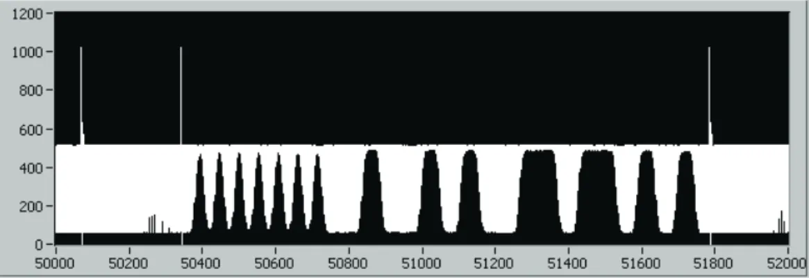
Figure 4. Line 21 Closed Caption ITU-R BT.656 Digital Output Capture with YUV Samples Present.
Raw Data Mode is Disabled.
Figure 5. Line 21 Closed Caption ITU-R BT.656 Digital Output Capture in Raw Data Mode.
UV (Chroma) Data are Replaced with Y (Luma) Data.
www.ti.com
Appendix A Subset of the TVP5147M1 VDP I
2C Registers
VDP Closed Caption Data Subaddress 80 051Ch - 80 051Fh
Subaddress 7 6 5 4 3 2 1 0
80 051Ch Closed Caption Field 1 byte 1
80 051Dh Closed Caption Field 1 byte 2
80 051Eh Closed Caption Field 2 byte 1
80 051Fh Closed Caption Field 2 byte 2
These registers contain the closed caption data arranged in bytes per field.
VDP WSS/CGMS Data Subaddress 80 0520h - 80 0526h WSS/CGMS NTSC: Read only Subaddress 7 6 5 4 3 2 1 0 Byte 80 0520h b5 b4 b4 b2 b1 b0 WSS/CGMS Field 1 byte 1 80 0521h b13 b12 b11 b10 b9 b8 b7 b6 WSS/CGMS Field 1 byte 2 80 0522h b19 b18 b17 b16 b15 b14 WSS/CGMS Field 1 byte 3 80 0523h Reserved 80 0524h b5 b4 b4 b2 b1 b0 WSS/CGMS Field 2 byte 1 80 0525h b13 b12 b11 b10 b9 b8 b7 b6 WSS/CGMS Field 2 byte 2 80 0526h b19 b18 b17 b16 b15 b14 WSS/CGMS Field 2 byte 3
These registers contain the wide screen signaling data for NTSC. Bits 0 - 1 Represent word 0, aspect ratio
Bits 2 - 5 Represent word 1, header code for word 2 Bits 6 - 13 Represent word 2, copy control
Bits 14 - 19 Represent word 3, CRC WSS/CGMS PAL/SECAM: Read only Subaddress 7 6 5 4 3 2 1 0 Byte 80 0520h b7 b6 b5 b4 b4 b2 b1 b0 WSS/CGMS Field 1 byte 1 80 0521h b13 b12 b11 b10 b9 b8 WSS/CGMS Field 1 byte 2 80 0522h Reserved 80 0523h Reserved 80 0524h b7 b6 b5 b4 b4 b2 b1 b0 WSS/CGMS Field 2 byte 1 80 0525h b13 b12 b11 b10 b9 b8 WSS/CGMS Field 2 byte 2 80 0526h Reserved
These registers contain the wide screen signaling data for PAL/SECAM: Bits 0 - 3 Represent group 1, aspect ratio
Bits 4 - 7 Represent group 2, enhanced services Bits 8 - 10 Represent group 3, subtitles
www.ti.com Appendix A
VDP VITC Data
Subaddress 80 052Ch - 80 0534h
Subaddress 7 6 5 4 3 2 1 0
80 052Ch VITC Frame byte 1
80 052Dh VITC Frame byte 2
80 052Eh VITC Seconds byte 1
80 052Fh VITC Seconds byte 2
80 0530h VITC Minutes byte 1
80 0531h VITC Minutes byte 2
80 0532h VITC Hours byte 1
80 0533h VITC Hours byte 2
80 0534h VITC CRC byte
These registers contain the VITC data.
VDP V-Chip TV Rating Block 1 Subaddress 80 0540h
Read only
7 6 5 4 3 2 1 0
Reserved 14-D PG-D Reserved MA-L 14-L PG-L Reserved
TV Parental Guidelines Rating Block 1
14-D: When incoming video program is "TV-14-D" rated, this bit is set high. PG-D: When incoming video program is "TV-PG-D" rated, this bit is set high. MA-L: When incoming video program is "TV-MA-L" rated, this bit is set high. 14-L: When incoming video program is "TV-14-L" rated, this bit is set high. PG-L: When incoming video program is "TV-PG-L" rated, this bit is set high.
VDP V-Chip TV Rating Block 2 Subaddress 80 0541h
Read only
7 6 5 4 3 2 1 0
Reserved 14-S PG-S Reserved MA-V 14-V PG-V Y7 - FV
TV Parental Guidelines Rating Block 2
MA-S: When incoming video program is "TV-MA-S" rated, this bit is set high. 14-S: When incoming video program is "TV-14-S" rated, this bit is set high. PG-S: When incoming video program is "TV-PG-S" rated, this bit is set high. MA-V: When incoming video program is "TV-MA-V" rated, this bit is set high. 14-V: When incoming video program is "TV-14-V" rated, this bit is set high. PG-V: When incoming video program is "TV-PG-S" rated, this bit is set high. Y7-FV: When incoming video program is "TV-Y7-FV" rated, this bit is set high.
Appendix A www.ti.com
VDP V-Chip TV Rating Block 3 Subaddress 80 0542h
Read only
7 6 5 4 3 2 1 0
None TV-MA TV-14 TV-PG TV-G TV-Y7 TV-Y None
TV Parental Guidelines Rating Block 3 None: No block intended
TV-MA: When incoming video program is "TV-MA" rated in TV parental guidelines rating, this bit is set high. TV-14: When incoming video program is "TV-14" rated in TV parental guidelines rating, this bit is set high. TV-PG: When incoming video program is "TV-PG" rated in TV parental guidelines rating, this bit is set high. TV-G: When incoming video program is "TV-G" rated in TV parental guidelines rating, this bit is set high. TV-Y7: When incoming video program is "TV-Y7" rated in TV parental guidelines rating, this bit is set high. TV-Y: When incoming video program is "TV-G" rated in TV parental guidelines rating, this bit is set high. None: No block intended
VDP V-Chip MPAA Rating Data Subaddress 80 0543h
Read only
7 6 5 4 3 2 1 0
Not Rated X NC-17 R PG-13 PG G N/A
MPAA Rating Block (E5h):
Not Rated: When incoming video program is "Not Rated" rated in MPAA rating, this bit is set high. X: When incoming video program is "X" rated in MPAA rating, this bit is set high. NC-17: When incoming video program is "NC-17" rated in MPAA rating, this bit is set high. R: When incoming video program is "R" rated in MPAA rating, this bit is set high. PG-13: When incoming video program is "PG-13" rated in MPAA rating, this bit is set high. PG: When incoming video program is "PG" rated in MPAA rating, this bit is set high. G: When incoming video program is "G" rated in MPAA rating, this bit is set high. N/A: When incoming video program is "N/A" rated in MPAA rating, this bit is set high.
www.ti.com Appendix A
VDP General Line-Mode and Line-Address Subaddress 80 0600h - 80 0611h
(default line mode = FFh, line address = 00h)
Subaddress 7 6 5 4 3 2 1 0 80 0600h Line address 1 80 0601h Line mode 1 80 0602h Line address 2 80 0603h Line mode 2 80 0604h Line address 3 80 0605h Line mode 3 80 0606h Line address 4 80 0607h Line mode 4 80 0608h Line address 5 80 0609h Line mode 5
80 060Ah Line address 6
80 060Bh Line mode 6
80 060Ch Line address 7
80 060Dh Line mode 7
80 060Eh Line address 8
80 060Fh Line mode 8
80 0610h Line address 9
80 0611h Line mode 9
Line address [7:0]: Line number to be processed by a VDP set by a line-mode register (default 00h) Line-mode register x [7:0]:
Bit 7 0 Disabled filters
1 Enabled filters for teletext and CC (null byte filter) (default) Bit 6 0 Send sliced VBI data to registers only (default)
1 Send sliced VBI data to FIFO and registers, teletext data only goes to FIFO. (default) Bit 5 0 Allow VBI data with errors in the FIFO
1 Do not allow VBI data with errors in the FIFO (default) Bit 4 0 Disabled error detection and correction
1 Enabled error detection and correction (teletext only) (default)
Bit 3 0 Field 1
1 Field 2 (default)
Bit [2:0] 000 Teletext (WST625, Chinese Teletext, NABTS 525) 001 CC (US, European, Japan, China)
010 WSS/CGMS (525, 625) 011 VITC
100 VPS (PAL only), EPG (NTSC only) 101 USER 1
110 USER 2
Appendix A www.ti.com VDP VPS, EPG Data Subaddress 80 0700h - 80 070Ch VPS: Read only Subaddress 7 6 5 4 3 2 1 0 80 0700h VPS byte 1 80 0701h VPS byte 2 80 0702h VPS byte 3 80 0703h VPS byte 4 80 0704h VPS byte 5 80 0705h VPS byte 6 80 0706h VPS byte 7 80 0707h VPS byte 8 80 0708h VPS byte 9 80 0709h VPS byte 10 80 070Ah VPS byte 11 80 070Bh VPS byte 12 80 070Ch VPS byte 13
These registers contain the entire VPS data line except the clock run-in code or the frame code. EPG:
Read Only
Subaddress 7 6 5 4 3 2 1 0
80 0700h EPG Frame Code
80 0701h EPG byte 1 80 0702h EPG byte 2 80 0703h EPG byte 3 80 0704h EPG byte 4 80 0705h Reserved 80 0706h Reserved 80 0707h Reserved 80 0708h Reserved 80 0709h Reserved 80 070Ah Reserved 80 070Bh Reserved 80 070Ch Reserved
VDP FIFO Output Control Subaddress C0h
Default (00h)
7 6 5 4 3 2 1 0
Reserved Host access enable
Host access enable: This register is programmed to allow host port access to the FIFO or allow all VDP data to go out the video port. 0 Output FIFO data to the video output Y[9:2] (default)
www.ti.com Appendix A
VDP Full-Field Enable Subaddress D9h Default (00h)
7 6 5 4 3 2 1 0
Reserved Full field enable
Full field enable:
0 Disable full field mode (default) 1 Enable full field mode
This register enables the full-field mode. In this mode, all lines outside the vertical blank area and all lines in the line-mode register programmed with FFh are sliced with the definition of register DAh. Values other than FFh in the line-mode registers allow a different slice mode for that particular line.
VDP Full-Field Mode Subaddress DAh Default (FFh)
7 6 5 4 3 2 1 0
Full field mode [7:0]
Full field mode [7:0]: This register programs the specific VBI standard for full-field mode. It can be any VBI standard. Individual line settings take priority over the full-field register. This allows each VBI line to be programmed independently but have the remaining lines in full-field mode. The full-field mode register has the same bits definition as line-mode register’s. (default FFh)
The global line mode has priority over the full-field mode.
VBUS Data Access with No VBUS Address Increment Subaddress E0h
Default (00h)
7 6 5 4 3 2 1 0
VBUS data [7:0] VBUS data [7:0]: VBUS data register for VBUS single byte read/write transaction.
VBUS Data Access with VBUS Address Increment Subaddress E1h
Default (00h)
7 6 5 4 3 2 1 0
VBUS data [7:0]
VBUS data [7:0]: VBUS data register for VBUS multi-byte read/write transaction. VBUS address is auto-incremented after each data byte read/write.
FIFO Read Data Subaddress E2h Read only
7 6 5 4 3 2 1 0
Appendix A www.ti.com
VBUS Address Access Subaddress E8h-EAh Default (00 0000h)
Subaddress 7 6 5 4 3 2 1 0
E8h VBUS address [7:0]
E9h VBUS address [15:8]
EAh VBUS address [23:16]
VBUS access address [23:0]: VBUS is a 24-bit wide internal bus. The user needs to program here the 24-bit address of the internal register to be accessed via host port indirect access mode.
Interrupt Raw Status 0 Subaddress F0h Read only
7 6 5 4 3 2 1 0
FIFO THRS TTX WSS/CGMS VPS/Gemstar VITC CC F2 CC F1 Line
FIFO THRS: FIFO Threshold passed, unmasked 0 Not passed
1 Passed
TTX: Teletext data available unmasked 0 Not available
1 Available
WWS/CGMS: WSS/CGMS data available unmasked 0 Not available
1 Available
VPS/Gemstar: VPS/Gemstar data available unmasked 0 Not available
1 available
VITC: VITC data available unmasked 0 Not available
1 Available
CC F2: CC field 2 data available unmasked 0 Not available
1 Available
CC F1: CC field 1 data available unmasked 0 Not available
1 Available
LINE: Line number interrupt unmasked 0 Not available
Available
www.ti.com Appendix A
Interrupt Clear 0 Subaddress F6h Default (00h)
7 6 5 4 3 2 1 0
FIFO THRS TTX WSS/CGMS VPS/Gemstar VITC CC F2 CC F1 Line
FIFO THRS: FIFO Threshold passed clear 0 No effect (default)
1 Clear FIFO_THRES bit in Status register 0 bit 7 TTX: Teletext data available clear
0 No effect (default)
1 Clear TTX available bit in Status register 0 bit 6 WSS/CGMS: WSS/CGMS data available clear
0 No effect (default)
1 Clear WSS available bit in Status register 0 bit 5 VPS/Gemstar: VPS/Gemstar data available clear
0 No effect (default)
1 Clear VPS available bit in Status register 0 bit 4 VITC: VITC data available clear
0 Disabled (default)
1 Clear VITC available bit in Status register 0 bit 3 CC F2: CC field 2 data available clear
0 Disabled (default)
1 Clear CC field 2 available bit in Status register 0 bit 2 CC F1: CC field 1 data available clear
0 Disabled (default)
1 Clear CC field 1 available bit in Status register 0 bit 1 Line: Line number interrupt clear
0 Disabled (default)
1 Clear Line interrupt available bit in Status register 0 bit 0
The host interrupt clear 0 and 1 registers are used by the external processor to clear the interrupt status bits in the host interrupt status 0 and 1 registers. When no non-masked interrupts remain set in the registers, the external interrupt pin will also become inactive.
///////////////////////////////////////////////////////////////////////////////////////// ////////////////////////////////////////////////////////
// These commands can be used with the WinVCC EVM software to configure the Line Mode // registers for a typical VBI setup.
// The WR_IND commands are VBUS indirect writes using the VBUS Address Access and
// VBUS Data Access registers. Each WR_IND command shown writes 1 byte to the VBUS
// address specified in the command line. BEGIN_DATASET
DATASET_NAME,"TVP5147M1 NTSC VDP/VBI SETUP"
// Use Indirect Registers to setup Line numbers and line mode
WR_IND,VID_DEC,0x01,0x800600h,0x0A // Select Line 10
WR_IND,VID_DEC,0x01,0x800601h,0x40 // Select teletext for Line 10 Field 1
WR_IND,VID_DEC,0x01,0x800602h,0x0A // Select Line 10
WR_IND,VID_DEC,0x01,0x800603h,0x48 // Select teletext for Line 10 Field 2
WR_IND,VID_DEC,0x01,0x800604h,0x15 // Select Line 21
WR_IND,VID_DEC,0x01,0x800605h,0x01 // Select Closed Caption for Line 21 Field1
WR_IND,VID_DEC,0x01,0x800606h,0x15 // Select Line 21
WR_IND,VID_DEC,0x01,0x800607h,0x09 // Select Closed Caption for Line 21 Field2
WR_IND,VID_DEC,0x01,0x800608h,0x0E // Select Line 14
WR_IND,VID_DEC,0x01,0x800609h,0x03 // Select VITC for Line 14 Field 1
WR_IND,VID_DEC,0x01,0x80060ch,0x14 // Select Line 20
WR_IND,VID_DEC,0x01,0x80060dh,0x02 // Select WSS/CGMS for Line 20 Field1
// Direct writes to I2C registers
WR_REG,VID_DEC,0x01,0xC0, 0x01 // Set host enable bit in register C0h to 1
// to enable FIFO access. END_DATASET
///////////////////////////////////////////////////////////////////////////////////////// ///////////////////////////////////////////////////////
www.ti.com
Appendix B Sample WinVCC CMD File for VBI Setup
www.ti.com
Appendix C VBI Raw Data I
2C Registers
Luminance Processing Control 1 Subaddress 06h
Default (00h)
7 6 5 4 3 2 1 0
Pedestal
Reserved Reserved VBI raw Luminance signal delay [3:0]
not present Pedestal not present:
0 7.5 IRE pedestal is present on the analog video input signal (default) 1 Pedestal is not present on the analog video input signal
VBI raw:
0 disable (default)
1 enable
Duration of the vertical blanking as defined by register 22h through 25h the chroma samples are replaced by luma samples. This feature may be used to support VBI processing done by an external device during the vertical blanking interval. In order to use this bit, the output format must be 10-bit ITU-R 656 mode.
Luma signal delay [3:0]: Luma signal delays respect to chroma signal in 1x pixel clock increments. 0111 Reserved
0110 6 pixel clocks delay 0001 1 pixel clocks delay 0000 0 pixel clocks delay (default) 1111 -1 pixel clocks delay 1000 -8 pixel clocks delay
VBLK Start Line Subaddress 22h-23h Default (001h) Subaddress 7 6 5 4 3 2 1 0 22h VBLK start [7:0] 23h Reserved VBLK start [9:8]
VBLK start [9:0]: This is an absolute line number. The TVP5147M1 device updates the VBLK start line only when the VBLK start MSB byte is written to. If user changed these registers, the TVP5147M1 retains values in different modes until device resets.
NTSC: default 001h PAL: default 623 (026Fh) VBLK Stop Line Subaddress 24h-25h Default (015h) Subaddress 7 6 5 4 3 2 1 0 24h VBLK stop [7:0] 25h Reserved VBLK stop [9:8]
VBLK stop [9:0]: This is an absolute line number. The TVP5147M1 device updates the VBLK stop only when the VBLK stop MSB byte is written to. If user changed these registers, the TVP5147M1 retains values in different modes until device resets.
IMPORTANT NOTICE
Texas Instruments Incorporated and its subsidiaries (TI) reserve the right to make corrections, modifications, enhancements, improvements, and other changes to its products and services at any time and to discontinue any product or service without notice. Customers should obtain the latest relevant information before placing orders and should verify that such information is current and complete. All products are sold subject to TI’s terms and conditions of sale supplied at the time of order acknowledgment.
TI warrants performance of its hardware products to the specifications applicable at the time of sale in accordance with TI’s standard warranty. Testing and other quality control techniques are used to the extent TI deems necessary to support this warranty. Except where mandated by government requirements, testing of all parameters of each product is not necessarily performed.
TI assumes no liability for applications assistance or customer product design. Customers are responsible for their products and applications using TI components. To minimize the risks associated with customer products and applications, customers should provide adequate design and operating safeguards.
TI does not warrant or represent that any license, either express or implied, is granted under any TI patent right, copyright, mask work right, or other TI intellectual property right relating to any combination, machine, or process in which TI products or services are used. Information published by TI regarding third-party products or services does not constitute a license from TI to use such products or services or a warranty or endorsement thereof. Use of such information may require a license from a third party under the patents or other intellectual property of the third party, or a license from TI under the patents or other intellectual property of TI.
Reproduction of TI information in TI data books or data sheets is permissible only if reproduction is without alteration and is accompanied by all associated warranties, conditions, limitations, and notices. Reproduction of this information with alteration is an unfair and deceptive business practice. TI is not responsible or liable for such altered documentation. Information of third parties may be subject to additional restrictions.
Resale of TI products or services with statements different from or beyond the parameters stated by TI for that product or service voids all express and any implied warranties for the associated TI product or service and is an unfair and deceptive business practice. TI is not responsible or liable for any such statements.
TI products are not authorized for use in safety-critical applications (such as life support) where a failure of the TI product would reasonably be expected to cause severe personal injury or death, unless officers of the parties have executed an agreement specifically governing such use. Buyers represent that they have all necessary expertise in the safety and regulatory ramifications of their applications, and acknowledge and agree that they are solely responsible for all legal, regulatory and safety-related requirements concerning their products and any use of TI products in such safety-critical applications, notwithstanding any applications-related information or support that may be provided by TI. Further, Buyers must fully indemnify TI and its representatives against any damages arising out of the use of TI products in such safety-critical applications.
TI products are neither designed nor intended for use in military/aerospace applications or environments unless the TI products are specifically designated by TI as military-grade or "enhanced plastic." Only products designated by TI as military-grade meet military specifications. Buyers acknowledge and agree that any such use of TI products which TI has not designated as military-grade is solely at the Buyer's risk, and that they are solely responsible for compliance with all legal and regulatory requirements in connection with such use. TI products are neither designed nor intended for use in automotive applications or environments unless the specific TI products are designated by TI as compliant with ISO/TS 16949 requirements. Buyers acknowledge and agree that, if they use any non-designated products in automotive applications, TI will not be responsible for any failure to meet such requirements.
Following are URLs where you can obtain information on other Texas Instruments products and application solutions:
Products Applications
Amplifiers amplifier.ti.com Audio www.ti.com/audio
Data Converters dataconverter.ti.com Automotive www.ti.com/automotive
DLP® Products www.dlp.com Communications and www.ti.com/communications
Telecom
DSP dsp.ti.com Computers and www.ti.com/computers
Peripherals
Clocks and Timers www.ti.com/clocks Consumer Electronics www.ti.com/consumer-apps
Interface interface.ti.com Energy www.ti.com/energy
Logic logic.ti.com Industrial www.ti.com/industrial
Power Mgmt power.ti.com Medical www.ti.com/medical
Microcontrollers microcontroller.ti.com Security www.ti.com/security
RFID www.ti-rfid.com Space, Avionics & www.ti.com/space-avionics-defense
Defense
RF/IF and ZigBee® Solutions www.ti.com/lprf Video and Imaging www.ti.com/video