2016 International Congress on Computation Algorithms in Engineering (ICCAE 2016) ISBN: 978-1-60595-386-1
1 INTRODUCTION
Measurement and control system occupies a major part in aerospace. In operation, measurement and con-trol system is responsible for several important tasks, such as target capture, target tracking, measurement data obtaining, and measurement data transmission. The system asks for high requirements for instantane-ity, accuracy and transmission rate in obtaining and transmitting measurement data [1]. The internal data transmission in current traditional measurement and control systems is mainly completed through Ethernet. However, there are disadvantages existing in the fol-lowing aspects of practical Ethernet application: (1) When network load is great, the online data transmis-sion delay on Ethernet is serious and unpredictable; (2) the completion of network communications needs many network protocols and thus can lead to reduction in through efficiency; (3) many equipment, such as switch and router, are required in data transmission. Abnormal equipment operation will result in failure to complete data transmission.
Based on the above disadvantages of Ethernet, we consider establishing reflective memory network [2]. The differences between reflective memory network and Ethernet are as follows:
(1) Data communications among each adjacent lay-er of OSI model are accomplished through Ethlay-ernet
software which requires CPU and thus are not con-venient for small-volume unexpected real-time data transmission. In reflective memory network, data communications are accomplished through hardware and thus no CPU time is needed. Moreover, the data packages in data communications through reflective memory network are very small which is beneficial for the transmission of unexpected data.
(2) Compared with those in reflective memory net-work, the transmission certainty, data predictability and support for interrupt signal transmission in Ether-net are in serious disadvantage due to the limit in Ethernet transmission mechanism.
(3) Reflective memory network contains more reli-able and improved hardware error diagnosis and pro-cessing mechanisms.
2 WORKING PRINCIPLES OF REFLECTIVE
MEMORY NETWORK
As a high-speed real-time network, reflective memory network allows using computers of various bus struc-tures and different operating systems to share real- time data with determined rate [3]. Reflective memory network is high in speed, light in host load, strong in software and hardware compatibility, convenient in use, reliable in transmission error correcting capability, and achievable in supporting interrupt signal transmis-sion.
The FPGA Design and Implementation of Reflective
Memory Card Based on the PCIE Bus
Zheng Bian, Lei Xie* & Botao Wu
China Satellite Maritime Tracking and Control Department, Jiangyin, Jiangsu, China
ABSTRACT: In order to solve the large-volume data problem in real-time transmission of measurement and control system, this paper proposed to use reflective memory network in measurement and control system. It studied the working principle and the topology structure of reflective memory network, and then suggested a hardware design method for reflective memory card. This method takes FPGA as its master control module of design. As the bus module, PCIE uses optical fibers for communication. In the end, this paper verified the effec-tiveness of the method and made the material object.
Keywords: reflective memory network; real-time network; FPGA
Reflective memory network is a special sharing memory system, aiming at sharing conventional data sets among multiple independent computers [4]. Re-flective memory network can store independent back-up of the overall shared memory in each subsystem [5]. Each subsystem can all enjoy sufficient access per-missions with no limit and can also modify local data sets with extremely high writing speed of local memory. When data is written in local reflective memory for backup, high-speed logic synchronization hardware will transmit the data to the next node of the loop network as shown in Figure 1. All computers are able to receive data written in reflective memory on the four nodes shown in the figure within a very short time. Each successive node can write new data in local backup at the same time and then transmit it to the next node in the loop network. Information will be deleted from the network once arriving on the initial node. Through specific hardware and node quantity, all computers in the network can own the same data in the same address within several microseconds. Local processors are able to read these data in random time without any internet access. Each computer can own the latest local backup of shared memory sets for good by this means.
Figure 1. Schematic diagram of reflective memory network.
Compared with traditional networks, reflective memory network owns the following advantages:
(1) Deterministic data transmission
Reflective memory is a network based on hardware. The data transmission among each network node en-tirely depends on hardware drive with no consumption of host CPU resources. All the data transmitted to some nodes is stored in local memory and automati-cally forwarded to the memory of other nodes in order. No software delay is involved in data transmission and all delay will just be caused by hardware.
(2) High data transmission speed
The requirement on real-time performance decides that reflective memory network must be able to
pro-vide high-speed service. Reflective memory network applies optical fiber connection and thus has high data transmission rate. Unit of reading/writing operation delay is only nanosecond. As a result, reflective memory network can significantly reduce total net-work communication delay and shorten netnet-work reac-tion period. Compared with those of most data net-works, the operation rate and information throughout of reflective memory network are much better.
(3) Easy to use
An ideal network shall allow all computers to visit the memory of each other at the same time. Reflective memory network is easy to use. Users only need to execute writing, reading and other simple operations through host software to complete the data sharing of the overall network. Due to global attribute of memory, several computers may visit memory at the same time. All the visits to common memory space written by CPU will be copied to other nodes of the network. Reflective memory will pellucidly monitor and copy the data, making it possible to share the data without any software overhead punishment.
(4) Operating system and individual processor Reflective memory hardware can be applied in VME, PCI/PCI-X, PMC, PCI Express and other vari-ous ports, allowing reflective memory network to be connected with different buses. No problem of byte exchange will occur even if reflective memory system is connected with computers of different byte formats (large port and small port). In addition, the exchange between large-port computer and small-port computer will not cause protocol overhead or loss of time.
(5) Technical superiority beyond LAN (local area network)
Compared with standard networks, reflective memory can provide more features, such as globalized memory, high-speed data transmission and software transparency. All these features can make reflective memory an attractive multi-computer communication solution, so as to solve the high-efficient interconnec-tion problem among computers [6].
3 PHYSICAL TOPOLOGY STRUCTURE OF
RE-FLECTIVE MEMORY NETWORK
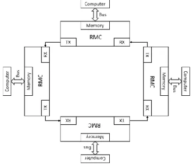
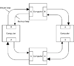
There are two main physical topology structures of reflective memory network: One is star topology structure as shown in Figure 2, and the other is loop topology structure as shown in Figure 3.
suc-cessive optical signals, eliminate insertion loss and solve the problem of cable signal attenuation. During signal regeneration, signal jitter will also be reduced. Moreover, star topology structure is simple in struc-ture, easy in control, and convenient in failure diagno-sis and fault isolation.
Loop topology structure is mainly in direct connec-tion with various reflective memory cards. Reflective memory loop structure can realize high-speed data transmission on optical fiber media. Unlike most Ethernet systems, loop topology structure is a system based on bus arbitration [7]. Therefore, this topology can avoid queuing and the complexity in checking data packages. Also, this topology can ensure correct connectivity with no additional load limit.
[image:3.516.265.463.293.413.2]In general, compared with star topology, loop to-pology is more suitable for reflective memory network. While using loop topology, a message packet is placed in the network and will circulate around the loop net-work until it is eliminated by source node. When a data package is eliminated by the node of source mes-sage (source elimination), the node can compare the returned messages with the original data one by one. Any difference can cause retransmission of the source message. The physical structure of loop topology can better fit high-real-time topical fiber technology.
[image:3.516.65.243.338.647.2]Figure 2. Star topology structure.
Figure 3. Loop topology structure.
4 SOFTWARE AND HARDWARE DESIGN OF
REFLECTIVE MEMORY CARD
4.1 Overall hardware design scheme
[image:3.516.76.232.513.653.2]According to the principle of reflective memory net-work, functional requirements and performance in-dexes of reflective memory card, the modularized design concept is used. The overall design of reflec-tive memory card hardware is shown in Figure 4, mainly including FPGA (register control, DMA, data transformation module and FIFO, etc.), memorizer [8], PCIE interface circuit, and optical fiber transmitting and receiving circuit. See Table 1 for the types of chip and equipment applied in each module. According to the functions which need to be accomplished inside FPGA, divide the internal logic of FPGA mainly into five modules as shown in Figure 5: PCIE endpoint, clock, memorizer, optical fiber communication and register. Clock module and register module are not lined out in the figure.
Table 1. Submodules included in each internal module of FPGA.
Module Types of chip and equipment
FPGA (including register control, DMA, data transformation module and FIFO, Module A)
Xilinx Spartan- 6(XC6SLX45T-FG484)
Optical fiber transmitting and receiving module (Module B)
-
PCIE module
(Module C) GF-PCIEXPS-X2
Memorizer (Module D) MT47H32M16HR-37EL(512MB)
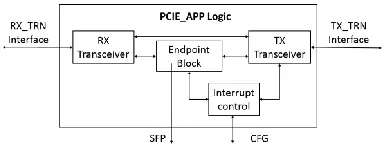
4.2 PCIE endpoint module
corre-sponding data can be responded to the computer. See Figure 6 for the overall situation.
Figure 6. Composition of PCI interface module.
4.3 Clock module
Clock module is used in the internal logic of timing FPGA. Reasonable clock design is the key in system design. There are two clock sources applied in this system: (1) a 50MHz difference clock crystal oscilla-tor from mainboard. After processing, the oscillaoscilla-tor can be used in PCIE hardcore module and memorizer module to execute relevant functions as shown in Figure 7. (2) A 125MHz difference clock crystal os-cillator used in GTP high-speed transceiver to
[image:4.516.121.397.193.275.2]com-plete optical fiber communications is shown in Figure 8 [10, 11].
Figure 7. 50MHz clock crystal oscillator circuit diagram.
4.4 Optical fiber communication module
Optical fiber communication module is responsible for the communication with SFP optical module as shown in Figure 9. It includes 5 submodules: GTP hardcore, PLL, DCM, data receiving module, and data transmis-sion module [12]. GTP is embedded in the high-speed receiver of XC6SLX45T to complete data coding and serial-parallel/parallel-serial conversion. A PLL and a DCM are respectively used to generate user clocks on transmitting end and receiving end. Data transmission Figure 4. General layout scheme of reflective memory card.
Figure 5. FPGA internal logical function of reflective memory card.
[image:4.516.59.252.331.404.2] [image:4.516.291.434.333.406.2] [image:4.516.63.458.555.656.2]module sends command to pack parameters according to user-defined protocol and send them to GTP. Data receiving module receives parallel data flow from GTP. It will extract related data and send it to FIFO for cache memory.
Figure 9. Schematic diagram of optical fiber communication module.
Reasonable clock design is the key to realize optical fiber communications. As the distribution and man-agement of GTP clock are complex, careful analysis must be made while designing. GTP reference clock uses 125MHz external clock crystal oscillator. Before entering GTP, IBUFDS is used in buffering treatment. A PLL can be used to generate TX end of GTP and clock of data transmission module. A DCM can be used to generate RX end of GTP and clock of data receiving module.
While customizing GTP, the selected REF-CLKOUT can be applied as the clock source of TX end. However, GTPCLKOUT [0] needs to be called while using REFCLKOUT. GTPCLKOUT [0] can generate two clocks after PLL processing: TXUSRCLK and TXUSRCLK2. TXUSRCLK is used in PCS-layer logic of TX while TXUSRCLK2 is used to synchronize TX interface and internal user logic of FPGA. Frequency of TXUSRCLK is determined by internal data width of GTP and rate of TX circuit. See (1) for the computational formula:
GTP Data Width
F =
TXUSRCLK Line rate (1)
The internal data width while using 8b/10b code is 10bit. When 8b/10b code is not in use, the internal data width is 8bit.
Frequency of TXUSRCLK2 is determined by TX data width and frequency of TXUSRCLK. There are three kinds of commonly-used TX data widths: 8bit, 16bit and 32bit. Corresponding computational formu-las are as follows:
F = F
TXUSRCLK2 TXUSRCLK (2)
FTXUSRCLK
F =
2
TXUSRCLK2 (3)
FTXUSRCLK
F =
4
TXUSRCLK2 (4)
The transmission rate of the optical fiber link in this
system is 2.5Gbps. Besides, 8b/10b code and 32bit of TX data width are used in this system. It can be con-cluded from the above computational methods that TXUSRCLK is 250MHz, TXUSRCLK2 is 62.5MHz and clock frequency of GTPCLKOUT [0] is 125MHz. As a result, twice frequency multiplication is needed for PLL to generate TXUSRCLK. 2-fractional fre-quency can generate TXUSRCLK2.
RX end of GTP receiver includes a clock reply cir-cuit. With the reference of local clock, the clock reply circuit can extract data information and clock RXRECCLK from inbound data stream. RXRECCLK can be directly used in the PCS-layer logic of RX; however, the application must involve indirect call of GTPCLKOUT [1]. This system uses a DCM module to generate the RXUSRCLK and RXUSRCLK2 of RX. The former one is used in the PCS logic layer of RX while the latter one is used to synchronize RX inter-face and the internal user logic of FPGA. The clock frequency of RXUSRCLK is the same with RXREC-CLK and can be directly outputted from DCM. Fre-quency of RXUSRCLK2 is related to RXUSRCLK and RX dada width of which the specific computa-tional method is similar to that of TXUSRCLK2. The difference between TX data width and RX data width is that the latter one applies 16bit. According to com-putation, frequency of RXUSRCLK2 is 125MHz. Therefore, RXUSRCLK2 can be obtained by realizing two-divided frequency of GTPCLKOUT [1] [15].
4.5 Register control module
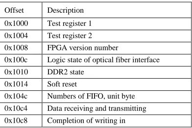
[image:5.516.266.462.481.612.2]There are two main functions that the control module of register can execute: One is to fulfill corresponding functions by controlling board card. Marks of corre-sponding offsets as shown in Table 2 are for the con-venience of software development. The other one is to accomplish user field processing as shown in Figure 10 [13].
Table 2. Offset function description.
Offset Description
0x1000 Test register 1
0x1004 Test register 2 0x1008 FPGA version number
0x100c Logic state of optical fiber interface 0x1010 DDR2 state
0x1014 Soft reset
0x104c Numbers of FIFO, unit byte 0x10c4 Data receiving and transmitting
0x10c8 Completion of writing in
Figure 10. Processing flow chart of user field.
(1) Delete data frame. When data frame passes through all nodes in loop network, it will return to the source node of transmission. Then, the source node shall confirm whether the frame has been transmitted from it or not by checking the source address field. If the data frame is confirmed, the source node will de-lete it from the network link and generate data deletion frame identification.
(2) Forward data frame. When there’s difference between the target address field and the physical ad-dress or broadcast adad-dress of current node, the current node needs to forward the frame and generate data forward frame identification.
(3) Store data frame. When the target address is the physical address or broadcast address of the current node, the current node needs to store the data and generate data storage frame identification.
5 SYSTEM DEBUGGING AND PERFORMANCE
ANALYSIS
5.1 Hardware circuit debugging
After manufacturing PCB of reflective memory card and completing welding of components and parts, debugging shall be accomplished for hardware circuit step by step. See Figure 11 for the completed material object. Before circuit board is powered on, conduct meticulous inspection on the board in comparison with the schematic diagram at first. For example, the circuit needs to be checked whether it is in short circuit, components need to be checked whether they are welded in a wrong way, and the power supply needs to be checked whether it is welded in a wrong way. After it is confirmed that no obvious mistake is made in the circuit, a power-on test shall be conducted. The supply voltage of each chip shall be tested for its correctness. Use an oscilloscope to check whether the clock is right. After finishing the inspection on basic circuit, further inspection on each chip to see whether they are in normal operation shall be conducted, such as FPGA
[image:6.516.289.434.95.165.2]download and FLASH download. Hardware circuit debugging can be considered as basically completed after all the above operational steps are finished.
Figure 11. Physical photo of reflective memory card.
5.2 FPGA logic debugging
Verilog design is used in all the logic programs inside FPGA. Development of the entire FPGA is accom-plished through ISE14.7, including simulation, syn-thetization, locating and writing, downloading, and debugging. Debugging of FPGA logic is usually com-pleted by using logic analyzer to observe internal sig-nal state. Traditiosig-nal logic asig-nalyzers are expensive and not convenient to use. The Xilinx used in this system can provide online logic analyzer ChipScope which includes debugging of PCIE application-layer logic and debugging of optical fiber module [14].
5.2.1 Logic debugging of PCIE application layer
After FPGA is downloaded, insert the reflective memory card into the mainboard slot of computer and start the computer. If the computer succeeds in start-up and the system device manager can detect a new device, it can be proved that PCIE interface is in a correct circuit, configuration of PCIE hardware is correct, and PCIE hardware is able to work normally. If any problem occurs, check the configuration pa-rameters of PCIE at first, and then check PCIE inter-face circuit. After the system can recognize the device, debugging can be conducted on PCIE applica-tion-layer logic.
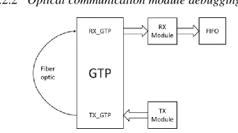
5.2.2 Optical communication module debugging
Figure 12. Optical fiber communication test system.
[image:6.516.270.441.494.590.2]com-munication test system. Self-defined regular data is generated from transmission module and transmitted through GTP transmit channel. Data is returned to the reception channel of GTP through optical fibers. Re-ceiving module is responsible for reRe-ceiving data and writing it into FIFO.
6 CONCLUSIONS
This paper introduced the working principle and its topology structure of reflective memory network, studied the superiorities of reflective memory network compared with traditional one, and proposed a hard-ware design method for reflective memory card. Re-al-time communication network is an important sub-ject in the development of aerospace tracking, teleme-try and command network. Reflective memory net-work is timely in communication, fast in data trans-mission and high in transtrans-mission reliability. It is an ideal technology to realize real-time system and thus can well fit the establishment of distributed real-time measurement and control network. There’s funda-mental practical significance contained in a thorough research on the application of reflective memory net-work on aerospace tracking, telemetry and command field.
REFERENCES
[1] Wu Z, Shan J F. & Xu H. 2013. A new real time data acquisition system for low hybrid current drive system. Proceedings of the 2012 International Conference on Communication, Electronics and Automation Engineer-ing Advances in Intelligent Systems and ComputEngineer-ing, 181: 299-303.
[2] Jovanovic M. & Milutinovic J. 1999. An overview of re-flective memory systems. Concurrency, IEEE, 7(2): 56-64.
[3] L. H. Arendt, P. Eng. 1998. A simple, high speed, low Latency reflective memory network for parallel pro-cessing systems. IEEE, 98: 209-212.
[4] Tao You, Chenglie Du & Yi’an Zhu. 2009. Supporting technology for virtual numerical control system based on RTX and reflective memory network.2009 Fifth Inter-national Conference on Natural Computation, pp: 319-323.
[5] Kenneth G. Lesueur. 2008. Encryption system for sup-porting hard real-time distributed testing. The ITEA
Journal of Test and Evaluation. Dec 2007/Jan pp:
131-134.
[6] M. Oguchi, H. Aida & T. Saito. 1995. A proposal for a DSM architecture suitable for a widely Ddistributed en-vironment and its evaluation. Proc. Fourth IEEE High Performance Distributed Computing (HPDC-4), IEEE CS Press, pp: 32-39.
[7] B. N. Bershad, M. J. Zekauskas & W. A. 1993. Sawdon. A midway distributed shared memory System. IEEE Computer Society Press, Los Alamitos, Calif. 4: 528 -537.
[8] Xilinx Inc. 2010. High-Performance DDR2 SDRAM In-terface in Spartan-6 Devices.
[9] Xilinx Inc. 2010. Spartan-6 FPGA Integrated Endpoint Block for PCI Express User Guide UG654 (v3.0). [10] Xilinx Inc. 2013. Spartan-6 FPGA Clocking Resources
User Guide UG382 (v1.9).
[11] Xilinx Inc. 2014. Spartan-6 FPGA Power Management User Guide UG394 (v1.2).
[12] Xilinx Inc. 2010. Spartan-6 FPGA GTP Transceivers User Guide UG386 (v2.2).
[13] Xilinx Inc. 2010. Spartan-6 FPGA Memory Controller User Guide UG388 (v2.3).
[14] Wenbo Xu & Geng Tian. 2015. Xilinx FPGA: Develop-ment and Application (2nd edition), Beijing: Tsinghua University Press.