CIO Asynchronous FIFO
Interface Programmer's
Guide
Flin-
HEWLETT
a:~ PACKARD
HP Part No. 27114·90003
Printed in USA September 1989
Contents
1. Introduction
U sing This Manual . . References . . . . Hardware Features Product Overview
Frontplane. . The Midplane . The Backplane .
2. AFI Theory of Operation
Overview . . . . Configuring the Device Adapter for an External Device
Handshake Signals . . . . .
PCTL Signal . . . . . PFLG Signal .
PDIR Signal . . . HEND Signal PEND Signal Handshaking Modes
FIFO-MASTER Handshake FULL.MASTER Handshake . FULL_SLAVE Handshake Interrupt Propagation. . . . Exclusive Access . . . . Transferring Data . . . .
Register Configuration . . . . . Read Configuration of Registers
Write Configuration of Registers
3. Using the AFI Device Adapter
Device 110 Library Interface . DIL Capabilities and Limitations . Direct Device Driver Interface . . .
Creating the Device File. . . Accessing the Device Adapter Releasing the Device Adapter Configuring the Device Adapter
Recommended Configuration Procedure . Locking the Device Adapter . . . .. . • Resetting the Device Adapter . . .
Setting the Timeout Value . . . . Setting the Data Path Width Value . . . .
Setting Additional Configuration Values . . 3-12 Setting the Logic Sense of PFLG . . . . 3-12 Setting the Handshake Mode. . . 3-13
Enabling the Data Transfer Counter 3-13
Enabling the PDIR and HEND Signals for the
External Device . . . 3-13 Enabling PEND Signal in Status Line. . . . 3-13 GPIOJ3ET_CONFIG Example. . . . . 3-13 Enabling and Disabling External Device Interrupts 3-14 Setting the Control Line Values . . . 3-15 Transferring Data . . . 3-16 Requesting Device Adapter Status Information . . 3-16
Returning the Process Id and Per-Device Adapter
Counter of a Locked Device Adapter . . 3-17 Returning the Timeout Value . . . . 3-17
Returning the Data Path Width Value 3-17
Returning Reason for Last Interrupt 3-18
Returning the Status Line Values. . . 3-18 Returning Device Adapter Specific Information . 3-19
Returning Multiple Status Values. . 3-20
Returning the Configuration Mask . . . . 3-21
Programmatic Example . . . 3-22
A. Error Code Values
Glossary
Index
Figures
Tables
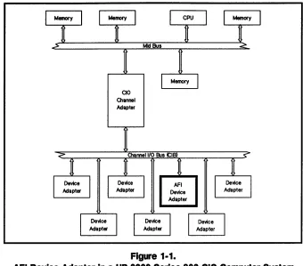
1-1. AFI Device Adapter in a HP 9000 Series 800 CIO
Computer System . . . 1-3
1-2. The AFI Device Adapter Planes . . 1-4 2-1. Frontplane Signals . . . 2-3 2-2. Input FIFO-MASTER Handshake . . . . 2-7
2-3. Output FIFO.MASTER Handshake 2-8
2-4. Input FULL-MASTER Handshake . 2-10
2-5. Output FULL-MASTER Handshake 2-11
2-6. Input FULLJ)LAVE Handshake . . . 2-13
2-7. Output FULL_SLAVE Handshake 2-14
2-8. External Device Interrupt Propagation Process . . 2-15 2-9. Registers on the Data Bus . . . . . . 2-18 2-10. Read Register 0: Input Data. . . . . 2-20 2-11. Read Register 1: CIO Sense. . . . 2-20 2-12. Read Register 3: CIO ID . . . . . 2-20 2-13. Read Register 7: Device Adapter Status. . 2-21 2-14. Read Register 9: CIO Status. . . 2-21 2-15. Read Register A: Transfer Counter . 2-21 2-16. Read Register B: Transfer Counter 2-22 2-17. Write Register 0: Output Data. . . 2-23 2-18. Write Register 1: CIO Control . . . 2-23 2-19. Write Register 7: Device Adapter Control . 2-23 2-20. Write Register A: Transfer Counter. . . . 2-24 2-21. Write Register B: Transfer Counter and Device
Adapter Control. . . . . 2-24 3-1. User Program Access Path Through DIL to Driver 3-1 3-2. User Program Access Path Direct to Driver . . . 3-3
1-1. Logic Sense of Frontplane Elements . . 2-1. External Device Requirement Table. . 2-2. Lock Counters Example . . . . 2-3. Register Configuration . ... . . . 3-1. Power Up and Reset Configuration Values .
1-5 2-2 2-17 2-18 3-10
Introduction
Using This Manual
1
This manual will guide you in writing detailed code needed to match features of the HP 27114B CIO Asynchronous FIFO Interface (AFI) Device Adapter to needs of your external device. CIO stands for Channel Input/Output.
Chapter 1, "Introduction," presents a list of primary features and a product overview that includes discussions and diagrams for the:
• Frontplane
• Midplane
• Backplane
Chapter 2, "AFI Theory of Opemtion," discusses configuring the AFI device adapter to an external device for transferring data. The following AFI device adapter features are discussed:
• Five configurable device dependent features
• Handshake signals
• Handshake modes
• Exclusive access
• Transferring data
• Read register configuration
• Write register configuration
Chapter 3, "Using the AFI Device Adapter," discusses accessing the AFI device driver, provides an ordered set of tasks for configuring and controlling the AFI device adapter, and provides a partial
programmatic example for each task and a full programming example at the end of the chapter.
A glossary at the end of the manual clarifies technical terms.
References
Hardware Features
1·2 Introduction
Additional information is contained in the following Hewlett-Packard manuals:
Asynchronous FIFO Interface Reference Manual (HP part number 27114-90004)
HP -UX System Administration Concepts Manual (HP part number 92594-90062)
HP -UX System Administration Tasks Manual (HP part number 92453-90038)
Concepts and Tutorials: Device I/O and User Interfacing (HP part number 97089-90054)
The AFI device adapter hardware features are:
• 16 bit parallel interface
Cl 16 bit frontplane data input lines
Cl 16 bit frontplane data output lines
• Differential or single-ended (with ground) signal drivers/receivers
• 64 words of FIFO. buffering
• Data transfer counter
• Midplane state machine to control handshaking
• Three handshaking modes
• Up to six frontplane control lines
• Up to six frontplane status lines
Product Overview
00 Channel
Adapter Mid Bus
Device Adapter
Figure 1·1.
AFI Device Adapter In a HP 9000 Series 800 CIO Computer System
The HP 27114B CIO Asynchronous FIFO Interface (AFI) Device Adapter provides buffered communications between external devices and HP 9000 Series 800 CIO systems using a single 64 word FIFO buffer. This device adapter is excellent for applications where high speed, 16 bit parallel transfers are required.
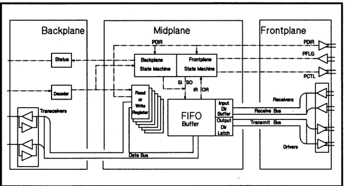
Figure 1-2 divides the design of the AFI device adapter into three planes of circuitry. They are:
• The frontplane (interacts with the external device and midplane)
• The midplane (interacts with the frontplane and backplane)
• The backplane (interacts with the channel adapter and midplane)
[image:8.612.215.555.72.371.2]Backplane Midplane Frontplane
ReceMn ~ ~-""'ReceIYe""""""-=-Sue---'
FIFO Buff., ~---:':::===--....I
Buffer (Mput Tf8IIIImlt Sue
~-,~~I~=~~I ~==~~~
L . . . - - - I
~~II
Figure 1·2. The AFI Device Adapter Planes
Each plane accepts data and control signals and converts them to the requirements of the CIO bus, the next plane, or the external device. To explain the operation of the planes, it is convenient to view the planes as working on logically independent tasks.
Frontplane
The frontplane controls or reacts to the external device and translates control signals to and from the midplane. The control signals combine in a handshake protocol with the external device to prevent data loss.1-4 Introduction
The following list contains the frontplane elements with the register representation and bit positions where 0 represents the least
significant bit.
• 16-bit Data Input Bus, RD[15:0] (RD[7:0] for 8-bit data)
• 16-bit Data Output Bus, SD[15:0] (SD[7:0] for 8-bit data)
• 6-bit Control Register, CTL[5:0]
• 6-bit Status Register, STS[5:0]
• 1 interrupt signal, ATTN
• 5 handshaking signals
1. Peripheral Control (PCTL)
2. Peripheral Flag (PFLG)
3. Transfer Direction (PDIR)
4. Host (handshake) End (HEND) - optional
[image:9.612.206.544.72.255.2]Note The PDIR, HEND, and ATTN signals are reflected by default in CTL[5:4] and STS[5] respectively.
This limits the number of control lines to 4 and status lines to 5. To enable all six lines for control or status you can programmatically override the default for each signal.
Frontplane handshaking signals control and monitor the sending and receiving of data to and from the external device.
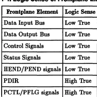
Low true logic means that assertion of the signal re:8.ects a low (0 V) state. High true logic means that assertion of the signal reflects a high (5 V) state.
To avoid confusion when discussing the assertion and deassertion of signals, Table l-llists frontplane elements and their default logic sense.
Table 1·1. Logic Sense of Frontplane Elements
Frontplane Element Logic Sense
Data Input Bus Low True
Data Output Bus Low True
Control Signals Low True
Status Signals Low True
HEND /PEND signals Low True
PDIR High True
PCTL/PFLG signals High True
The Asynchronous FIFO Interface Reference Manual explains the logic sense and signal propagation between the hardware and software domains. The reference manual also discusses how to physically change the default logic sense of frontplane elements by crossing differential lines to external device (if the external device is differential) or by grounding one line and connecting the other to the external device (if the external device is single-ended).
Determining the logic sense of front plane elements for your AFI device adapter is critical for configuring external device dependent features, data transfers, and interpreting status lines.
[image:10.615.308.469.299.460.2]The Midplane The midplane circuitry includes:
• the FIFO buffer and associated control circuitry
• the data, status, and control registers
• the handshake control state machine
Logically there are two state machines on the AFI device adapter. One handles data transfers between the FIFO and the front plane and the other handles data transfers between the backplane and the FIFO.
The Backplane The backplane contains the I/O channel interface control circuitry that controls communications between the AFI device adapter and the channel I/O bus.
2
AFI Theory of Operation
Overview
Configuring the
Device Adapter for
an External Device
Note
Interfacing with the AFI device adapter is divided into three categories:
1. Configuring the device adapter for an external device
2. Obtaining exclusive access to the device adapter
3. Transferring data
The following sections describe the device adapter operation with respect to the numbered categories listed above.
There are nine configurable AFI device adapter attributes that are configurable for external device compatibility:
1. data path width
2. logic sense of PFLG
3. handshaking mode
4. enable or disable interrupts from external device
5. number of control lines
*
6. enable PDIR and HEND signals for external device
7. control lines value
8. number of status lines
*
9. enable PEND signal from external device
By default, the attributes marked by an appended
"*,,
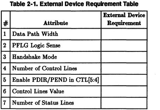
are limited to 4 or 5 lines but are programmatically configurable to 6 lines.The Asynchronous FIFO Interface Reference Manual presents an explanation of how to connect AFI device adapters to several external devices. There is a table in the AFI hardware reference manual to fill in that defines the necessary AFI device adapter configurations to consider for proper operation and use of the
intended external device. Values from this table should be applied to setting the appropriate values and flags through the gpioO device driver. The gpioO device driver interface is described in section 7 of the HP-UX Reference Manual indexed by gpio.
Table 2-1 is a copy of the table found in the AFI hardware reference manual. You may find it more convenient to copy or fill in the values in the following table and work from this table.
Table 2-1. External Device Requirement Table
External Device
#
Attribute Requirement1 Data Path Width
2 PFLG Logic Sense
3 Handshake Mode
4 Number of Control Lines
5 Enable PDIR/PEND in CTL[5:4]
6 Control Lines VaIue
7 Number of Status Lines
To configure the AFI device adapter for an external device you must understand the three following AFI device adapter features and their
operation:
• Handshake signals
• Handshaking overview with timing diagrams
• Interrupt propagation
In addition to the above listed device adapter features, the sections that follow discuss obtaining exclusive access to the device adapter and the transferring of data.
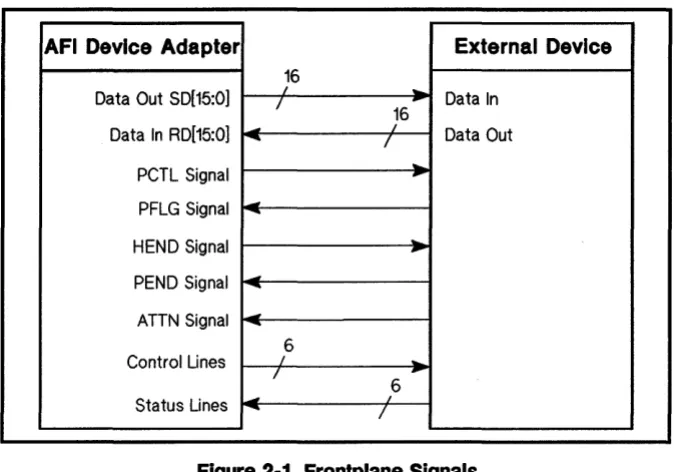
Handshake Signals The following five signals are used for handshakes during a data transfer.
1. PCTL (Peripheral Control)
2. PFLG (Peripheral Flag)
3. PDIR (Peripheral Direction)
4. HEND (Host End)
5. PEND (Peripheral End)
Figure 2-1 shows the source and destination of these five signals.
Note
AFI Device Adapter External Device 16
Data Out 5D[15:0] /
,
-
-
Data In 16Data In RD[15:0]
--
-
I,
Data OutPCTl Signal
-
rPFlG Signal
-
--HEND Signal
..
-PEND Signal
-
--ATTN Signal
--
--6
Control Lines I
-I
-Status Lines
-
,6--- I
Figure 2·1. Frontplane Signals
peTl Signal
The assertion of PCTL (peripheral control) means that the outgoing data are· valid or that new incoming data can be accepted. For the FIFO ..MASTER and FULL..MASTER handshaking modes, the device adapter asserts PCTL to signal readiness to start a data transfer. For FULL..8LAVE handshake mode, the device adapter asserts PCTL after the PFLG (Peripheral Flag) signal is received from the external device.
PFlG Signal
The external device asserts PFLG (peripheral flag) signal to inform the AFI device adapter that the external device has accepted the data transferred or that there are valid incoming data from the device. For incoming data there is at least one CIO bus clock pulse before data transfer is complete.
The EDGE.LOGIC_SENSE flag selects the logic sense of the PFLG signal as high true or low true. It is the handshake mode selection that interprets the edge or level state to be the PFLG signal.
The default, EDGE.LOGIC_SENSE flag deasserted, defines the rising edge or level state (5 V) of PFLG to signal the device adapter. The assertion of EDGE.LOGIC_SENSE flag defines the falling edge or low level state (0 V) of PFLG to signal the device adapter.
The handshake timing diagrams assume theEDGE.LOGIC_SENSE flag is deasserted. .
[image:14.613.220.557.71.307.2]Note
Note
Note
2·4 AFI Theory of Operation
PDIR Signal
The PDIR (peripheral direction) signal informs the external device which direction to perform the data transfer, incoming or outgoing. PDIR is set by the read and write system calls used for requesting a data transfer. Assertion of PDIR indicates the data transfer is an outgoing write request and the deassertion of PDIR indicated the data transfer is an incoming read request.
To enable the device adapter to send the PDIR signal to the external device the PDIR_OPT-EN flag must be asserted. By default the PDIR_OPT-EN flag is asserted. The PDIR signal is sent in CTL[5].
Assertion of PDIR_OPT-EN Hag limits the number of control lines to 4, CTL[3:0]. CTL[5:4] contain the PDIR and REND signals respectively.
The HP 27114A "DIR" signal is renamed "PDIR". Although the operation is identical, the "PDIR" name better describes the signal.
HEND Signal
The AFI device adapter can be enabled to assert the REND (host end) signal when the last word of data is being transferred. To enable the device adapter to send the REND signal to the external device during a read or a write data transfer, the PDIR_OPT-EN flag must be asserted. By default the PDIR_OPT-EN flag is asserted. The REND signal is sent in CTL[4].
Assertion of PDIR_OPT-EN Hag limits the number of control lines to 4, CTL[3:0]. CTL[5:4] contain the PDIR and REND signals respectively.
See the handshake timing diagrams for specific timing of the REND signal.
PEND Signal
The external device asserts the PEND (peripheral end) signal to inform the device adapter that the last word of data is being transferred. To enable the device adapter to recognize the PEND signal from the external device during a data transfer the PEND_OPT-EN flag must be asserted.
For example, a read request is submitted from the device adapter for 30 words of data. If the external device only has 20 words, at the end of the 20th word PEND is asserted to inform the device adapter that the last . word of data is being sent. If PEND_OPT -EN is not ·asserted, the device adapter will not recognize the PEND signal
Note
Handshaking Modes
Note
By default the PEND_OPT..EN flag is deasserted enabling status information in STS[4]. When PEND_OPT..EN flag is asserted the PEND signal is acknowledged in STS[4].
Assertion of PEND_OPT..EN limits the number of status lines to 4 or 5. If PEND_OPT..EN is asserted, STS[4] reflects the PEND signal. If interrupts are enabled STS[5] contains the ATTN signal which limits the number of status lines to 4, STS[3:0] respectively. If interrupts are disabled, STS[5] is available for reflecting status information and the number of status line are limited to 5, STS[5] and STS[3:0] respecti vely.
AFI device adapter handshake modes provide any of three handshake protocols, illustrated in Figures 2-2 through 2-7:
• FIFO-MASTER Mode
• FULL-MASTER Mode
• FULL-SLAVE Mode
The handshaking modes are device dependent.
The HP 27114A PULSE-HANDSHAKE-MODE has been renamed FIFO-MASTER. Although the operation is identical, the "FIFO" name better describes the handshake.
The following sections describe each of the handshake modes in detail. Timing diagrams and a detailed sequence of events are presented for the input and output data transfer direction for each handshake mode.
2·6 AFI Theory of Operation
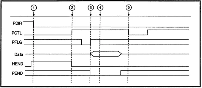
FIFO..MASTER Handshake
For the FIFO-MASTER handshake, when data is valid, the data transfer occurs on the edge transition of PFLG. The PFLG edge transition is configured with the GPIO-SET _CONFIG function, EDGE-LOGIC-SENSE flag. When the EDGE-LOGIC-SENSE flag is asserted, data transfer occurs on the asserted-to-deasserted transition trailing edge of PFLG. When the EDGE-LOGIC-SENSE flag is deasserted (default), data transfer occurs on the
deasserted-to-asserted transition leading edge of PFLG.
Note
®
®
@®
! ! ! I
I I I I I
I I I I
I I I I
I I I I
I I
I
I , PD1RIp e T l : ;-
---;::==========::::;---;:::=========
I I
I
PFlG_+i ____
--+----1'----1I I I
I
k
Data - I ! - - - i i - - - f '
I
I I I I
HEND
.-J!
I
I
PEND
-i-! ---;-.----,
I I I : I j I I
>
I [image:18.612.221.560.76.224.2]:
I I I , I:
I :Figure 2·2. Input FIFO..MASTER Handshake
The FIFO..MASTER input handshake has the following signal sequence:
1. Device adapter deasserts PDIR (read request)
2. Device adapter asserts PCTL regardless of PFLG state
3. External device asserts PFLG (data valid and stable)
4. External device deasserts PFLG after minimum duration as configured in the hardware or PFLG may remain asserted
5. Device adapter deasserts PCTL after recognizing PFLG assertion and receiving data
Steps 2 through 5 above are repeated until last word is to be read. The last word transfer sequence is as follows:
1. PDIR remains deasserted
2. Device adapter asserts PCTL / asserts HEND (low)
3. External device asserts PFLG / asserts PEND (low)
4. External device deasserts PFLG or PFLG may remain asserted
5. Device adapter deasserts PCTL
Steps 4 above are not required to happen before step 5 for input FIFO..MASTER handshake.
Note
Note
2·8 AFI Theory of Operation
CD
@®
00
®
f
If
,
t
f
,
I I I I I
PDIR
.-J
I I I : I II I
I I I I
I
I
II
peTl I I
I I
I I I I
PFlG
:
:
I
:
I I I I I
Data
--K=:=>k
!
!>Ie><
I I : I :
I
I
IHEND~ I I I I
I I I I
I I I I I
I
I
I
I IPEND I I I
I I I
I I I I I
I I I I I
: : : : :
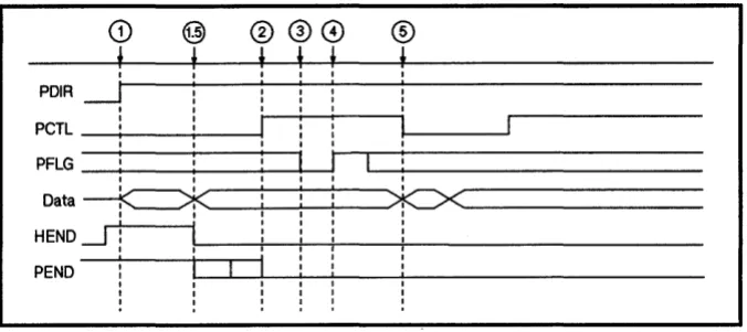
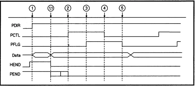
Figure 2·3. Output FIFO..MASTER Handshake
The FIFO..MASTER output handshake has the following signal sequence:
1. Device adapter asserts PDIR (write request)
2. Device adapter asserts PCTL reguardless of PFLG state ( data is valid when PDIR and PCTL are asserted)
3. External device deasserts PFLG edge (data may be transferred)
4. External device asserts PFLG edge (data may be transferred)
5. Device adapter deasserts PCTL (data is invalid)
Steps 2 through 5 above are repeated until last word is to be written. The last word transfer sequence is as follows:
1. PDIR remains asserted
1.5. Device adapter asserts REND (low)
2. Device adapter asserts PCTL / asserts REND (low)
3. External device deasserts PFLG
4. External device asserts PFLG
5. Device adapter deasserts PCTL
Steps 3 above can occur before steps 1 or 2 above, but must occur before steps 4 above for output FIFO..MASTER handshake.
PEND may be asserted by the external device if it has received the required data. If PEND is asserted low prior to the device adapter asserting PCTL, the transfer does not take place.
The PEND_OPT..EN flag must be asserted for the device adapter to recognize the PEND signal from the external device.
[image:19.613.206.544.73.223.2]Note
device, the device adapter will wait until the external device accepts all the data or a timeout occurs.
FULL~ASTER Handshake
For the FULL..MASTER handshake, when data is valid, the data transfer occurs when the external device signal PFLG is in a stable state. The PFLG state that triggers data to be transferred is configured with the GPIO..8ET _CONFIG, EDGE.LOGIC..8ENSE flag. When the EDGE.LOGIC..8ENSE flag is asserted, data transfer occurs upon the PFLG signal stabilizing in a low (0 V) state. When the EDGE.LOGIC..8ENSE :flag is deasserted, the default, data transfer occurs upon the PFLG signal stabilizing in a high (5 V) state.
The difference between FIFO..MASTER and FULL..MASTER handshakes are the PFLG requirements. For the FULL..MASTER handshake, the level state of PFLG is checked where the
FIFO..MASTER handshake checks for the edge transition.
For the FULL..MASTER handshake the device adapter checks for deasserted state of PFLG before asserting PCTL to start the handshake. After PCTL is asserted, the external device asserts PFLG. The device adapter deasserts PCTL in response to the PFLG assertion. The external device then deasserts PFLG in response to the PCTL deassertion. Tlie duration of the PCTL and PFLG signals are dependent on each other.
2·10 AFI Theory of Operation
I I I I I
PDIR - , 1 - - - - -... : - -... : - - - -__ I : ___ : _ _ _ _ _
I I I I
I I
I I
r---peTl _-'--_ _ _ - - - ' : l . . - . - _ ... ; _ _ _ ...J1
PFlG _~ _ _ _ _ _ _
-II
I
I I
Data
-+---i---i<!C---)>--+----+!---I I
HEND~
I--_~:~---~--+:---PEND
i
!I I
I I
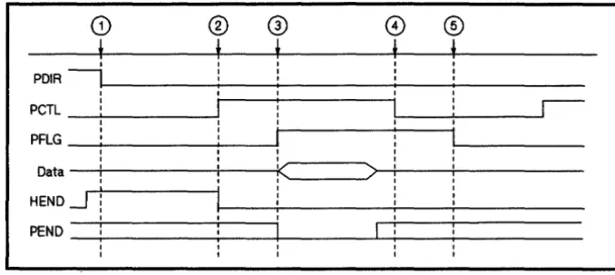
Figure 2·4. Input FULL-MASTER Handshake
The FULL-MASTER input handshake has the following signal sequence:
1. Device adapter deasserts PDIR (read request)
(device adapter waits for PFLG to be in a deasserted state)
2. Device adapter asserts PCTL
3. External device asserts PFLG to acknowledge PCTL
4. Device adapter deasserts PCTL to acknowledge PFLG
5. External device deasserts PFLG to end handshake and enable next transfer
Steps 2 through 5 above are repeated until last word is to be read. The last word transfer sequence is as follows:
1. PDIR remains asserted
(device adapter waits for PFLG to be in a deasserted state)
2. Device adapter asserts PCTL / asserts HEND (low)
3. External device asserts PFLG / asserts PEND (low)
4. Device adapter deasserts PCTL
[image:21.617.204.543.75.226.2]Note
CD
@
®
@
8)®
~ L , , , ,
I I I I I
I I : : I
PDIR ~t---i__--+:---i-: - -... : i
-I I I I
peTl -....;...: _ _
+--_--11
:
I
: I I I
PFLG _ ... : _ _ -:--_-+-~
---Ii
I : I
I - -_ _ _ _ _ - - J
r
~~~
__
~!i---~!--~--+~x~---HEND
--.J
!
! - i_--+: __
+! _ _ +-_-+-_ _ _ _ _ _ _PEND: 1 - 1
----L-4i---i-!
i i [image:22.612.224.562.76.229.2]-I ! I
Figure 2·5. Output FULL..MASTER Handshake
The FULL MASTER output handshake has the following signal sequence:
1. Device adapter asserts PDIR (write request)
(device adapter waits for PFLG to be in a deasserted state)
2. Device adapter asserts PCTL
3. External device asserts PFLG to acknowledge PCTL
4. Device adapter deasserts PCTL to acknowledge PFLG
5. External device deasserts PFLG to end handshake and enable next transfer
Steps 2 through 5 above are repeated until last word is to be written. The last word transfer sequence is as follows:
1. PD IR remains asserted
(device adapter waits for PFLG to be in a deasserted state)
1.1. Device adapter asserts HEND (low)
2. Device adapter asserts PCTL
3. External device asserts PFLG
4. Device adapter deasserts PCTL
5. External device deasserts PFLG
PEND may be asserted by the external device if it has received the required data. If PEND is asserted low prior to the device adapter asserting PCTL, the transfer does not take place.
The PEND_OPT-EN flag must be asserted for the device adapter to recognize the PEND signal from the external device.
If the PEND_OPT-EN flag is.deaSserted and the device adapter has more data to· send.· after PEND has been asserted by the external device, the device adapter will wait until the external device accepts all the data or a timeout occurs.
2·12 AFI Theory of Operation
FULL_SLAVE Handshake
For the FULL-SLAVE handshake, when data is valid, the data transfer occurs when device adapter has recognized the PFLG by asserting the PCTL signal. The GPIO-SET_CONFIG function, EDGE..LOGIC-SENSE flag configures the PFLG state that triggers the data transfer.
For the FULL-SLAVE handshake, the device adapter PCTL signal is dependent upon receiving the external device PFLG signal. When the external device PFLG signal is received stating that the external device is ready to transfer data, the device adapter acknowledges the PFLG signal by asserting PCTL and the data transfer occurs. The external device deasserts PFLG to invalidate the data on the bus and the device adapter acknowledges the PFLG deassertion with the deassertion of PCTL which terminates the handshake.
CD®
®
0
®
®
~ ~ ~ ~ ~ ~
: I I I :
I I I
I I : I I
PDIRI I I I I I I I
I I I I
I I I I I
PCTL I I I I i I
I
I Ir
I I I I
I I I I I
PFLG I I
I
I
I II
: I
I I I I
I
k
>l
t!(
>--Data I
I I I
HEND~
!
I I II I I
I I I
I I I
PEND
i
II
r==
I
[image:24.615.221.559.76.227.2]I ! I
Figure 2·6. Input FULL_SLAVE Handshake
The FULLJ)LAVE input handshake has the following signal sequence:
1. Device adapter deasserts PDIR (read request)
2. External device asserts PFLG
3. Device adapter asserts PCTL
4. External device deasserts PFLG
5. Device adapter deasserts PCTL
Steps 2 through 5 above are repeated until last word is to be read . The last word transfer sequence is as follows:
1. PDIR remains deasserted
2. External device asserts PFLG / deasserts PEND (high)
3. Device adapter asserts PCTL / asserts HEND (low)
4. External device deasserts PFLG / deasserts PEND (high)
5. Device adapter deasserts PCTL
6. External device asserts PEND (low)
Note
Note
2·14 AFI Theory of Operation
Q)(g) ~ ~
C9
~~ ~ ~
t
t
t
I I
PDIR
I
I
I
PCTL
!
i
I
PFLG
I
i
i
II
!
Data
!
1<*
!
I
><1
HEND ..-I
!
!
i
PEND
I I I
[image:25.617.205.541.75.237.2]!
!
Figure 2·7. Output FULL_SLAVE Handshake
The FULL..8LAVE output handshake has the following signal sequence:
1. External device asserts PFLG
2. Device adapter asserts PDIR (write request) 3. Device adapter asserts PCTL
4. External device deasserts PFLG 5. Device adapter deasserts PCTL
Steps 1 through 5 above are repeated until last word is to be transferred. The last word transfer sequence is as follows:
1. External device asserts PFLG 2. PDIR remains asserted
2.1. Device adapter asserts REND (low)
3. Device adapter asserts PCTL 4. External device deasserts PFLG 5. Device adapter deasserts PCTL
r
-Steps 1 above could occur after steps 2 above, but before steps 3 above, for output FULL_SLAVE handshake.
PEND may be asserted by the external device if it has received the required data. If PEND is asserted low prior to the device adapter asserting PCTL, the transfer does not take place.
The PEND_OPT-EN flag must be asserted for the device adapter to recognize the PEND signal from the external device.
Interrupt Propagation
Note
Note
The ATTN (attention) signal is an asynchronous interrupt from the external device. Enabling and disabling interrupts enable or disable the device adapter to acknowledge the ATTN signal on the frontplane. Interrupts are enabled and disabled with the GPIO..8IGNAL..MASK function. While interrupts are enabled, the ATTN signal is reflected in STS[5].
Enabling interrupts limits the number of status lines available. If the PEND_OPT-EN flag is asserted, reflecting the PEND signal in STS[4], and interrupts are enabled, the number of status lines are limited to 4, STS[3:0] respectively. If the PEND_OPT-EN flag is deasserted and interrupts are enabled, the number of status lines are limited to 5, STS[4:0] respectively.
For the AFI device adapter, the only front plane interrupt possible is the assertion of ATTN by the external device that propagates through the AFI device adapter, backplane, gpioO device driver, and finally sent to the process as a SIGEMT signal. Figure 2-8 illustrates the propagation of the interrupt from the external device to the process. The interrupt signal propagation occurs independently of the handshaking and data transfer operations on the AFI device adapter.
HP 9000
---HP:.-UX---
Series 800API DevIoe Ad.pter
____________________ J
backp...
mlclplane. frontpl ....• •
• • • • • • •
- - - -:-..; - - - i 4 - - - t
: ATTN
External
[image:26.613.221.560.374.659.2]Device
Figure 2·8. External Device Interrupt Propagation Process
If interrupts are enabled you should use the signal system call to trap the SIGEMT signal sent by the gpioO device driver. The signal system call is described.in section 2 of the HP-UX Reference Manual.
Exclusive Access
2·16 AFI Theory of Operation
To guarantee exclusive access to the device adapter it must be locked. When a process locks the device adapter, all subsequent requests are denied and the requesting processes are suspended until the device adapter is unlocked or until the timeout value of the requesting process is reached. When a device adapter is unlocked and there are suspended processes waiting on the device adapter, these processes simultaneously wake up to resubmit their lock request. Only one process is given permission to lock the device adapter and subsequent requests to lock the device adapter are suspended again. There is no method for determining which process, of many awakened from a suspended state, is permitted to lock the device adapter next.
A process may open the device adapter several times, thus creating several file descriptors. A process may also lock a device adapter several times without unlocking it between lock requests. Multiple open and lock sequences affect the lock counters value returned upon a successful lock request.
The device driver increments two types of lock counters upon a successful lock:
• a per-device adapter counter
The per-device adapter lock counter increments each time a particular process locks the device adapter.
• a per-open counter
A per-open lock counter is kept for each file descriptor
created by the open system call. The per-open counter associated with a particular file descriptor increments in addition
to the per-device adapter counter.
Transferring Data
Note
[image:28.618.227.556.110.249.2]For example, Table 2-2 displays the counter values as a particular sequence of open and lock requests are initiated.
Table 2·2. Lock Counters Example
Sequence Per-Device Adapter Per-Open Counter Per-Open Counter
of Calls Counter £d(A) fd(B)
open (fd A) 0 0 0
lock (fd A) 1 1 0
lock (fd A) 2 2 0
open (fd B) 2 2 0
lock (fd B) 3 2 1
Upon completion of a successful lock the per-open counter associated with the particular file descriptor is returned in arg[l] and the current per-device adapter counter is returned in arg[2].
Both counters decrement on an GPIO..LOCK, UNLOCK-INTERFACE request. The GPIO..LOCK,
CLEAR..ALL..LOCKS request resets the per-device adapter counter and the associated per-open counter( s) to zero.
Transfer data with the read and write HP-UX system calls. The read and write system calls are described in section 2 of the HP-UX
Reference Manual.
Before you attempt to read or write to any device adapter, you should lock the device adapter to ensure exclusive access.
The gpioO device driver logically changes on-board register
configuration depending on the direction of data transfer. The second part of this section discusses two register configurations for a device adapter read and write data transfers.
Register Configuration The on-board logical register configuration changes upon a read or write request. Table 2-3 lists the register number and the associated functionality upon a read or write data transfer. Figure 2-9 illustrates the AFI device adapter registers on the bus.
Table 2·3. Register Configuration
Register
Number Read Write
0 input data output data
1 CIO sense reg CIO control reg
3 CIO ID reg (not used)
7 device adapter status reg device adapter control
9 CIO status reg (not used)
A transfer counter transfer counter
B transfer counter transfer counter and device adapter control
r---l
~
0246Q
~ ~
b;J
i
I-'----~___I~~~-~~~~l[
I
L ______________________________________________________ ---l
Figure 2·9. Registers on the Data Bus
Read Configuration of The read resisters contain the following information: Registers Register
Note
0: input data register. The CIO bus reads a data word from this register.
1: CIO SENSE register. This register contains the interrupt pending signal bit, ARQ, and the interrupt enable signal bit ARE.
3: CIO ID register. This register contains the interface ID and revision number.
7: device adapter status register. This register contains the six status bits, the handshaking signal bits, and FIFO status. FIFO status indicates: if data exists in the FIFO and if there is room for more data, count of
remaining space for data, PEND, HEND, ATTN, and ZERO signals.
9: CIO status register. This register contains a set value to be read to clear the ARQ bit.
A: transfer counter register. This register contains the low and middle bytes of the transfer counter.
B: transfer counter register. This register contains the high byte of the transfer counter.
The transfer counter is 3 bytes long. Register A contains the middle and lower bytes of the transfer counter while Register B contains the upper byte of the transfer counter. The lower byte of the B Register is not used for a read request.
The following diagrams show the bit values of each of the read registers.
ffi M 0 ~
n
ro
9 8 :---r---r---r---l---r---l---i---~1 DATA : DATA : DATA : DATA : DATA : DATA : DATA : DATA
!
: . _________________________________________________________________ 1 _________ I I I 1 I 1 : 1
7 6 5 4 3 2 1 0
:---r---l---l---T---r---T---l---:
l~:~:~:~:~:~:~:~!
l _________
L ________ J _________ J _________ l _________ L ________ 1 _________ 1 _________ :Figure 2-10. Read Register 0: Input Data
15 14 13 12 11 10 9 8
:---r---r---r---l---r---l---i---~
: I I I I I I I
l
: 0 I 0 I 0 I 0 I 0 1 0 1 0 I 0 :
: I I I 1 I 1 :
. _________________________________________________________________ 1 _________ 1
7 6 5 4 3 2 1 0
:---r---l---l---T---r---T---I---:
1 1 : 1 : 0 : 0 : 1 : ARE: 0 : ARQ
!
l _________
L ________ J _________ J _________ l _________ L ________ 1 _________ 1 _________ :Figure 2-11. Read Register 1: CIO Sense
15 14 13 12 11 10 9 8
~---r----~----r---r---l---r---l---l---~
l
I I I I I I Il
: 0 I 0 I 0 I 0 I 0 I RV2 I RV1 I RVO :
: I I I I I I :
. ___________________________________________________________________ 1 _________ 1
7 6 5 4 3 2 1 0
:---r---l---l---T---r---T---I---:
l
0 1 0 1 1 I 0 I 0 1 0 1 0 1 0l
: I I I I I I I :
• L I I L •
[image:31.612.207.543.77.224.2]: _____________________________________ 1 _________________ 1 _________ 1 _________ :
Figure 2-12. Read Register 3: CIO ID
[image:31.612.206.544.78.416.2]15 14 13 12 11 10 9
a
:---r---r---r---,---r---,---1---
11 I I I I I STS5 I STS4 I 1
: HF I AEF I PEND I ATTN I ZERO I (ATTN) I (PEND) I STS3 :
l _________
L ________ J _________ J _________ l _________ L ________ l _________ l _________ !7 6 5 4 3 2 1 0
:---r---1---1---1---r---1---1---:
i
PCTL : PFLG: OR : IR : HEND : STS2 : STS1 : STSOi
[image:32.618.205.559.71.614.2]L ________ L ________ J _________ J _________ 1 _________ L ________ 1 _________ 1 _________ :
Figure 2-13. Read Register 7: Device Adapter Status
~ M 0 ~ fl
m
9 8:---r---r---r---,---r---,---1---
1: I I I I I I I 1
: 0 I 0 I 0 I 0 I 0 1 0 1 0 I 0 :
: _________ L
________ J _________ J _________ 1 _________ L
________ l _________
l _________ !7 6 5 4 3 2 1 0
:---r---1---1---1---r---1---1---:
1 0 1 0 1 0 1 1 1 0 1 0 1 0 1 0 :
: I I I I I I I :
: _________ L ________ J _________ J _________ 1 _________ L ________ 1 _________ 1 _________ :
Figure 2-14. Read Register 9: CIO Status
15 14 13 12 11 10 9 a
r---r---r---r---,---r---,---1---
1: I I I I I I I :
: TC15 I TC14 I TC13 I TC12 I TC11 I TC10 I TC9 I Tca :
: _________ L
________
J _________ J _________1 _________ L
________ l _________
l _________ !7 6 5 4 3 2 1 0
:---r---l---l---T---r---1---1---:
1~1~1~1~1~1~1 wl~l
: _________ L ________
J _________
J _________ 1 _________ L ________ 1 _________ 1 _________ :Figure 2-15. Read Register A: Transfer Counter
[image:32.618.220.556.75.225.2]ffi M a ~ n ID 9 8
:---r---r---r---l---r---l---i---~
: I I I I I I I :
: TC23 I TC22 I TC21 I TC20 I TC19 I TC18 I TC17 I TC16 :
: _________ L
________ J _________ J _________ 1 _________
L
________
1 _________
1 _________ :7 6 5 4 3 2 1 0
:---r---l---l---T---r---1---T---:
: 0 I 0 I 0 I 0 I 0 1 0 1 0 I 0
l
: I I I I I I I :
[image:33.615.203.545.74.221.2]: _________ L _________ '- ________ J _________ 1 _________ L ________ 1 _________ 1 _________ :
Figure 2·16. Read Register B: Transfer Counter
Write Configuration of
The write resisters contain the following information:Registers
RegisterNote
2·22 AFI Theory of Operation
0: output data register. This register contains a data word to be put into the FIFO and ultimately put on the device adapter frontplane data lines for the external device.
1: CIO control register. This register contains the DeL, DEN, ARE, and ARD bit values.
7: Device Adapter control register. This register contains the six control bits and other internal values.
A: transfer counter register. This register contains the low and middle bytes of the transfer counter.
B: transfer counter register. This register contains the high byte of the transfer counter, bits to
define the handshake mode, PDIR_OPT-EN bit, the interrupt enable bit, counter reset bit, and the PEND reset bits.
The transfer counter is 3 bytes long. Register A contains the middle and lower bytes of the transfer counter while Register B contains the upper byte of the transfer counter and device adapter control information.
ffi M 0 ~ ~
ro
9 8:---r---r---r---,---r---,---i---~
: I I I I I I I :
!~I~I~I~I~I~I~I~:
! _________
L
________
J _________ J _________1 _________ L
________ 1 _________
1 _________ :7 6 5 4 3 2 1 0
:---r---1---1---r---r---T---j---:
: I I I I I I I :
!~I~I~I~I~I~I~I~:
[image:34.615.223.561.73.613.2]l _________
L ________ J _________ J _________ 1 _________ L ________ 1 _________ 1 _________ :Figure 2·17. Write Register 0: Output Data
15 14 13 12 11 10 9 8
:---r---r---r---,---r---'---i---~
! I I I I I I I !
: x
Ix
Ix
Ix
Ix
Ix
Ix
Ix :
! _________
L
________
J _________ J _________1 _________ L
________ 1 _________
1 _________ :7 6 5 4 3 2 1 0
:---r---1---1---T---r---T---~-j---:
j
x : x :
DCl : DEN :x : x :
ARE : ARD j: _________ L ________ J _________ J _________ 1 _________ L ________ 1 _________ 1 _________ :
Figure 2·18. Write Register 1: CIO Control
ffi M 0 ~ ~
ro
9 8I---r---r---r---,---r---,---:
: cr~ cru I I
: x
I PNDD I ZROD I X I lCNT I or I or I CTl3 !: I I I I I (PDIR) I (HEND) I :
: _________ L
________
J _________ J _________1 _________ L
________ 1 _________
1 _________ :7 6 5 4 3 2 1 0
:---r---1---1---T---r---T---j---:
: PREN I PDIR I EDGE I ClF I PEN I CTl2 I CTl1 I CTlO :
: I I I I I I I :
: _________ L ________ J _________ J _________ 1 _________ L ________ 1 _________ 1 _________ :
Figure 2·19. Write Register 7: Device Adapter Control
2·24 AFI Theory of Operation
~ M
a
~ fl ID 9 8:---r---r---r---l---r---l---l---~
: I I I I I I I :
:~I~I~I~I~I~I~I~:
! _________ L
________
J _________ J _________1 _________ L
________ 1 _________
1 _________ :7 6 5 4 3 2 1 0
:---r---l---l---r---r---1---1---:
1 TC7 : TC6 : TC5 : TC4 : TC3 : TC2: TC1 : TCO 1
[image:35.617.204.548.75.432.2]: _________ L ________ J _________ J _________ 1 _________ L ________ 1 _________ 1 _________ :
Figure 2·20. Write Register A: Transfer Counter
15 14 13 12 11 10 9 8
:---r---r---r---,---r---l---l---~
: I I I I I I I :
: TC23 I TC22 I TC21 I TC20 I TC19 I TC18 I TC17 I TC16 :
: I I J I I I :
1 __________________________________________________________________ 1 _________ 1
7 6 5 4 3 2 1 0
:---r---l---l---r---r---~----1---1---:
1 ATEN : OREN : CNTR : PENR:
x :
MODE2: MODE1: MODEO 1: _________ L
________
J _________ J _________1 _________ L
________ 1 _________ 1 _________ :
Figure 2·21.
3
Using the AFI Device Adapter
Device I/O Library
Interface
There are two methods for accessing the AFI device driver, gpioO:
1. Calling Device I/O Library (DIL) subroutines to interface with the driver.
2. Interacting with the driver directly.
The Device I/O Library (DIL) is a set of user accessible subroutines that simplify the interface between user written code and a device adapter. You must programmatically include the header file gpio.h
to define the structures needed to talk to the AFI device adapter. The header file links are created with the C language #include statement. The DIL is locat'ed in the /usr/lib/libdvio. a library. Once written, compile the program and interactively link it to the DIL by entering:
[image:36.617.224.561.457.696.2]cc filename. c -ldvio
Figure 3-1 shows the user access path to the AFI driver through the DIL.
HP-UX Operating System
Include
Files 1---1
I I
I=--=--i
i=--=~
:gp~~~ -=--_r .... Library
Programs \
1---
C?>.~\,D.I.L.,~ ~
I=--i
Unk~j==--=--l
'=--=--1
'=--=--1
j==--=--l
I I
1 _ _ _ ----1
B
User Applications
i-Prog~~~
L ___ ----!
Driver Driver Driver
; - - - - r
-Other Other Other
Card Card Card
' - - - - ' - - - - '
-Figure 3-1. User Program Access Path Through OIL to Driver
DIL Capabilities and
Limitations
For further information on using the DIL to access the AFI device driver, see the Concepts and Tutorials: Device I/O and User Interfacing.
While the DIL provides a common interface to communicate with device adapters, it does not allow configuration of all the AFI device adapter features.
You can use the DIL subroutines to:
• Lock and unlock the device adapter
• Reset the device adapter
• Set a timeout for transactions
• Set data path width
• Enable or disable interrupts
• Set the control lines
• Return the status lines value
You cannot use the DIL subroutines to:
• Set the edge logic sense of PFLG
• Select handshake mode.
• Enable transfer counter
• Enable PDIR and HEND flags for the external device
• Enable PEND flag value in status line
• Return process id and per-device adapter counter of a locked process
• Return the timeout value
• Return the data path width value
• Return the reason for the last interrupt
• Return device adapter specific information
• Return multiple status values in one call
• Return the configuration mask containing:
o logic sense of PFLG
o current handshake mode
o transfer counter configuration
o PDIR and HEND signals configuration
o PEND signal configuration
Direct Device Driver
Interface
There are several steps to using the AFI device adapter:
1. Creating the device file
2. Accessing and releasing the device adapter
3. Configuring the device adapter operation
4. Transferring data
[image:38.615.222.559.220.465.2]5. Requesting device adapter status information
Figure 3-2 shows the user access path to the AFI driver directly.
HP-UX Operating System
Include Files
,---,
1=--=--,
j=-
~-~ #include,gplo.h:
~;;ry~
Programs
r----'
,D.I.L. I
i=--=--i
1=--=--,
1=--=--,
1=--=--,
1=--=--,
I I
,----!
User Applications
Driver Driver
r
-§
OtherCard Card
-i-prog~~~
!...---!
Driver
§
CardFigure 3·2. User Program Access Path Direct to Driver
Creating the Device File The first step in accessing the AFI device adapter is to create a device file. This file modifies the original configuration file created when the computer system was installed. Create a file named gpioO
in the I dev directory with the mknod, make node, command. The
mknod command description is found in section 1M of the the
HP- UX Reference Manual. For example, the following command specifies the filename to be created, character type device, the major number of 22, and the minor number of O~
1. mknod I dev I gpioO c 22 OxO
Accessing the Device Adapter
Note
For multiple AFI device adapters and AFI device adapter-to-AFI device adapter communication, the minor number must be changed for each device file. All the examples in this manual assume you have created a device file named / dev / gpioO. Refer to the HP 9000 Series 800: System Administration Tasks Manual for specifics on creating
device files.
The second step in accessing the AFI device adapter is to
communicate with'the device adapter via the logically associated device file. The HP -UX operating system treats devices as files using the open system call on the device files to gain and release access
respectively. The open call returns the file descriptor (fd) as an integer that uniquely identifies the device adapter to the process. All operations on a particular device adapter must specify the fd value. The open system call is described in section 2 of the HP- UX
Reference Manual. The open system call syntax is as follows:
int fd, oflag; char *path;
fd
=
open(path,oflag); where:fd path oflag
file descriptor
specifies the device file to be opened specifies the access mode
OJtDONLY for reading only O_WRONLY for writing only OJtDWR for reading and writing
For example, the following open call opens the device file for reading and writing to the device adapter.
int fd, of lag; char *path;
fd
=
open(lI/dev/gpioll,O_RDWR);If you do not want the process to suspend upon a lock request to a currently locked device adapter, the 0 ~D ELAY flag must be set in the open call. The O~DELAY file status flag is set in the open call by Oiling this flag with the access mode. For example, the following open call sets the O~DELAY flag:
oflag
=
O_NDELAY I O_RDWR; fd=
open(path,oflag);Executing an open call does not guarantee exclusive access to the device adapter. The device adapter must be locked if you require exclusive access; see the "Locking the Device Adapter" section of this chapter.
Releasing the Device Adapter
Configuring the Device Adapter
After you have finished your I/O operations, use the close system call to release access to the device adapter. The close system call is described in section 2 of the HP- UX Reference Manual. The close system call syntax is as follows:
int fd; close(fd);
where:
fd identifies the device adapter file descriptor you wish to release.
Use the ioctZ system call to configure device adapter attributes. The ioctl system call is described in section 2 of the HP- UX Reference M anuaZ. The ioctZ system call syntax is as follows:
int ret_val, fd, OP_CATGRY; struct io_ctl_status *OP_STRUCT;
ret_val
=
ioctl(fd, OP_CATGRY, OP_STRUCT);where: ret_val
fd
the status value returned after the operation request.
o
=
successful operation -1=
failureinteger value that uniquely identifies the device adapter you wish to operate.
OP _CATGRY specifies operation category (status or control).
OP ..8TRUCT is the data structure associated with the specified OP _CATGRY.
If the ioctl fails, indicated by a -1 value in ret_val, you can use the errno system call function to return a code indicating the reason for the failure. Refer to Appendix A for a list of possible errno return values. The errno system call is described in' section 2 of the HP- UX
Reference ManuaZ.
AFI device adapter ioctl operations are specified in the OP _CATGRY parameter and separated into three categories:
• IO_CONTROL. These operations pass various configuration
parameters to the device adapter. The 10_CONTROL structure includes the following fields:
struct io_ctl_status
{
int type;
1
* control request command*1
int arg[3];I*parameters to be passed*1 } gpio_control;
.• IO_STATUS. These operations request status information on a single device adapter parameter. See the "Requesting Device Adapter Status Information" section of this chapter. The 10-STATUS structure includes the following fields:
struct io_ctl_status
{
int type; I*status request command*1 int arg[3];I*parameter to be received*1 } gpio_status;
• IO_ENVIRONMENT. This operation requests information on several device adapter parameters and returns their values in one structure. See the "Requesting Device Adapter Status Information" section of this chapter. The 10 ..ENVIRO NMENT structure includes the following fields:
struct io_environment
{
int interface_type int timeout;
1*
status of linesSTS[5:0]*1
int status;
1*
reason for last interrupt*1
int signal_mask;1*
data path width*1
int width;1*
locking process id*1
int locking_pid;I*from GPIO_SET_CONFIG
*1
unsigned int config_mask;} gpio_env;
The type field of the control and status structures tell the driver the particular configuration request or status request to perform. The
. arg field of the control and status structures. contains a set of three integer parameters.
Each ioctl system call passes.the configuration or status request and the associated structure containing parameters to the gpioO device driver.
Note
The header file gpio.h defines the io.£tLstatus and the io..environment structures in addition to the IO_CONTROL, IO_STATUS, and IO..ENVIRONMENT variables.
Recommended Configuration Procedure
The IO_CONTROL configurations should be performed in the following sequence after successfully opening the appropriate device file:
It is recommended that you request the current configuration values with GPIO_GET_CONFIG and preserve them before reconfiguring new values.
1. Lock the device adapter (GPIO..LOCK)
2. Reset the device adapter (GPIO..RESET)
3. Set the timeout value for transactions (GPIO_TIMEOUT)
*
(Jel( opeN4. Set the data path width value (GPIO_WIDTH)
5. Set additional configuration values (GPIO-SET_CONFIG)
set logic sense of PFLG set handshake mode
enable data transfer counter
enable PDIR and HEND flags for external device enable PEND flag in a status line, STS[4]
6. Enable or disable interrupts (GPIO-SIGNAL..MASK)
7. Set the control lines value (GPIO_CTL..LINES)
Note
Note
AFI configurable attributes are classified into two groups:
1. Per-device adapter
The per-devIce adapter configurations affect all file descriptors associated with a particular device adapter.
2. Per-open
The per-open configurations affect only the file descriptor initiating the request.
The per-open configurations are noted in the above recommended configuration procedure by an appended asterisk
'*'.
The remaining configurations are per-device adapter requests.The IOJ)TATUS requests have no specific order to be performed except before GPIO..8ET_CONFIG if prior configuration values are to be preserved.
For all of the programmatic examples that follow, the parameters IO_CONTROL, IOJ)TATUS, and IO_ENVIRONMENT are defined in the gpio.h header file that you should include in your program.
Locking the Device Adapter
The GPIQ..LOCK function locks or unlocks the device adapter. Once locked, only the locking process can write to or read from the device adapter. Any other process may open the device adapter, but trying to write to or read from the locked device adapter will suspend the process until the lock is removed or until a timeout occurs. However, if the O~DELAY file flag is set, a process will not suspend if the device adapter is currently locked. Instead, the "device adapter currently locked" value, EACCESS, is returned in ret_val and the process resumes execution.
The O~DELAY file flag is set during the open system call, see the "Accessing and Releasing the Device Adapter" section of this chapter.
A per-device adapter counter and a per-open counter increment upon a successful lock. For clarification of these counters see Chapter 2 of this manual. Both counters decrement on an GPIO..LOCK, UNLOCK.1NTERFACE function request. The GPIO..LOCK,
CLEAR-ALL..LOCKS function resets the counters to zero. When the count is zero, any process can access the device adapter. Parameters passed to lock and unlock the device adapter:
type arg[O]
arg[2:1]
GPIO..LOCK
LOCK.1NTERFACE or UNLOCK.1NTERFACEor CLEAR-ALL..LOCKS
not used
Parameters returned from a successful GPIO..LOCK function:
arg[O] arg[l] arg[2]
not used
value of the per-open counter
value of the per-device adapter counter
For example, to lock a device adapter:
int fd;
struct io_ctl_status gpio_control; gpio_control.type
=
GPIO_LOCK;1*
lock device adapter*1
gpio_control.arg[O]
=
LOCK_INTERFACE;ret_val
=
ioctl(fd, IO_CONTROL, tgpio_control);ReseHing the Device Adapter
[image:45.617.237.531.132.423.2]The GPIO..RESET function resets all hardware and hardware related software device adapter settings to their default values. Table 3-1 lists the power up and reset default values.
Table 3·1. Power Up and Reset Configuration values
Attribute Power Up Value
Timeout 1 hour
Interrupt Deasserted
Locking locks clear
Control lines 000000
Data path width 16 bits
EDGE-LOGIC-SENSE Deasserted
Handshake mode FIFO-MASTER
TRNSFR-CTR..EN Deasserted
PDIR_OPT _EN Asserted
PEND_OPT..EN Deasserted
Data path value unknown
PDIR (direction) Deasserted -read
Parameters passed to reset the device adapter:
arg[O] arg[2:1]
HW_CLR not used
Reset Value
unaltered
Deasserted
unaltered
000000
unaltered
Deasserted
FIFO-MASTER
Deasserted
Asserted
Deasserted
value unknown
Deasserted -read
GPIO..RESET does not return parameters to the calling process.
For example, to reset the device adapter:
3·10 Using the AFI Device Adapter
int fd;
struct io~ctl_status gpio_control; gpio_control.type
=
GPIO_RESET; gpio_control.arg[O]=
HW_CLR;Setting the nmeout value
The GPIO_TIMEOUT function sets the software timeout value for a transaction. Any DMA activity lasting longer than the time defined in arg[O] microseconds (p,) seconds will abort and return a status of ETIMEDOUT in ret_val. Parameters passed to set the timeout value:
type arg[O]
GPIO_TIMEOUT
number of microseconds before a timeout occurs. (default 1 hour)
[2:1] not used
The arg[O] value is rounded up to the next 10 p, seconds.
GPIO_TIMEOUT does not return parameters to the calling process.
For example, to set the timeout to 1 second:
int fd;
struct io_ctl_status gpio_control; gpio_control.type
=
GPIO_TlMEOUT;1*
one second*1
gpio_control.arg[O]
=
1000000;ret_val
=
ioctl(fd, IO_CONTROL, &gpio_control);Setting the Data Path Width value
The GPIO_WIDTH function sets the width of the device adapter data path. The value of arg[O] must be either 8 or 16. H the width is 16, the transfer length and the buffer address specified in the read or write must be even because each transaction involves two bytes, otherwise, the error code EFAULT is returned in ret_val. These restrictions are based on hardware limitations of the channel adapter. Parameters passed to set the data path width:
type arg[O]
arg[2:1]
GPIO_WIDTH
data path width (8 or 16) (default 16)
not used
GPIO_WIDTH does not return parameters to the calling process.
For example, to set the data path width:
int fd;
struct io_ctl_status gpio_control; gpio_control.type
=
GPIO_WIDTH;1*
data path is 16 bits vide*1
gpio_control.arg[O]
=
16;ret_val
=
ioctl(fd, IO_CONTROL, &gpio_control);Note
Setting Additional Configuration values
The GPIOJ)ET_CONFIG function is used to:
• set the logic sense of PFLG
• set the handshaking modes
• enable and disable the transfer counter
• enable control lines CTL[5:4] for PDIR and REND signals
• enable status line STS[4] to reflect the PEND signal
The configuration of these attributes is accomplished by bitwise ORing a list of flags to pass' in the arg[O] parameter.
Each GPIO_SET _CONFIG function overwrites the previous
configuration. To retrieve the old configuration use the IO_STATUS, GPIO_GET_CONFIG request combination.
Parameters passed to set the flag values of GPIO_SET_CONFIG:
type GPIO-SET _CONFIG
arg[O] flag mask - result of ~Ring the flag values together arg[2:1] not used
GPIO-SET_CONFIG does not return parameters to the calling process.
Setting the Logic Sense of PFLG. The GPIO_SET_CONFIG function configures the edge logic sense of the PFLG signal from the external device by asserting or deasserting the EDGE..LOGIC-SENSE flag.
The deassertion of EDGE..LOGIC_SENSE flag, the default, has the following affects on the handshaking modes:
• FIFO ..MASTER. The rising edge of PFLG triggers the data transfer.
• FULL..MASTER. The stabilization of the transitioning PFLG to a high (5 V) state triggers the data transfer.
• FULL_SLAVE. The stabilization of the transitioning PFLG to a high (5 V) state initiates the handshake sequence.
The assertion of EDGE.LOGIC_SENSE has the following affects on the handshaking modes:
• FIFO..MASTER. The falling edge of PFLG triggers the data transfer.
• FULL..MASTER. The stabilization of the transitioning PFLG to a low (0 V) state triggers the data transfer.
• FULL_SLAVE. The stabilization of the transitioning .PFLG to a low (0 V) state initiates the handshake sequence.
Note
Note
SeUlng the Handshake Mode. The GPIO..sET _CONFIG function sets the handshake mode. The handshake mode is device dependent. The possible handshake mode flags are:
• FIFO..MASTER (default)
• FULL..MASTER
• SLAVE..MASTER
The HP 27114A PULSE.JIANDSHAKE..MODE has been renamed FIFO..MASTER. Although the operation is identical, the "FIFO" name better describes the handshake.
See Chapter 2 for timing diagrams and clarification of the three handshake modes.
Enabling the Data Transfer Counter. The GPIO..sET _CONFIG function enables the data transfer counter by asserting the
TRNSFR_CTR-EN flag. The transfer counter monitors the number of words put in the 66 word FIFO buffer. This ensures the device adapter only accepts the requested amount of data into the FIFO and transferred. Default is TRNSFR_CTR-EN deasserted.
Enabling the transfer counter is recommended.
Enabling the PDIR and HEND Signals for the External Device. The GPIO_SET _CONFIG function enables control lines 5 and 6, CTL[5:4], to reflect the current values of the PDIR and REND signals respectively by asserting the PDIR_OPT -EN flag. Default is PDIR_OPT-EN flag asserted.
Enabling PEND Signal in Status Line. The GPIO..sET_CONFIG function enables the PEND signal to be reflected in status line 5, STS[4], by asserting the PEND_OPT-EN flag. Default is PEND_OPT -EN flag deasserted and STS[4] reflects status information.
GPIO_SET _CONFIG Example. Suppose the following configurations:
• set the falling edge of PFLG to trigger data transfer
• set the handshake mode to FULL..MASTER
• enable the transfer counter
• enable PDIR and HEND values on the control lines, CTL[5:4]
• enable device adapter to recognize the PEND signal in STS[4]
The following example performs the above configurations:
Note
int fd;
struct io_ctl_status gpio_control; gpio_control.type
=
GPIO_SET_CONFIG;gpio_control.arg[O]
=
(EDGE_LOGIC_SENSEI
FULL_MASTERI
TRNSFR_CTR_EN
I
PDIR_OPT_EN PEND_OPT_EN)ret_val
=
ioctl(fd, 1