HP 27130A
EIGHT -CHANNEL MUL TIPLEXER
(MUX)
HEWLETT-PACKARD COMPANY Roseville Networks Division
8000 Foothills Boulevard
Technical Reference Manual
Flin-
HEWLETT
~I!.I PACKARDCard Assembly: 5061-4929 Date Code: A-2301
The Printing History below identifies the Edition of this Manual and any Updates that are included. Periodically, update packages are distributed which contain replacement pages to be merged into the manual, including an updated copy of this Printing History page. Also, the update may contain write-in instructions.
Each reprinting of this manual will incorporate all past updates; however, no new informa-tion will be added. Thus, the reprinted copy will be identical in contenf.to prior printings of the same edition with its user-inserted update information. New editions of this
manual will contain new information, as well as updates.
First Edition ... June 1983
NOTICE
The information contained in this document is subject to change without notice.
HEWLETT-PACKARD MAKES NO WARRANTY OF ANY KIND WITH REGARD TO THIS MATERIAL, INCLUDING, BUT NOT LIMITED TO, THE IMPLIED WARRANTIES
OF MERCHANTABILITY AND FITNESS FOR A PARTICULAR PURPOSE.
Hewlett-Packard shall not be liable for errors contained herein or for incidental or con-sequential damages in connection with the furnishing, performance, or use of this material.
CONTENTS
Section I
Page
GENERAL INFORMATION
PhY5icai De5cription .•.•..•••.••.••••••.•••••.••.•••••.•••...••.. 1-1
Functional Description ....• ·.;, •.•..•...•..•...•... 1-1
Equipment Supplied . . . 1-3
Identification . . . 1-3
The Product .... ~ . . . 1-3
Printed Circuit Card ....••...•.•.••••....•..••...•.•.••.•.•••.. 1-3
fw1a.nua15 ..••.•.•••••...••••••.••.••••••.••••••••••••••••.••••••• 1-4 Specifications . . . 1-4
Section II
INSTALLATION
Page
Determining Current Requirements .•.•.•...••••.••.•••..••••••.•... 2-1
Firmware (EPROM> In5tallation ....•••.•.•.••••.•.••..•.••..••.•... 2-1
Jumpe r 5 • • • • • • • • • • • • • • • • • • • • • • • • • • • • • • • • • • • • • • • • • • • • • • • • • • • • • • • • • • 2 - 3
Memory Configuration Jumper •.•...•...•...•...••...
2-3Signature AnalY5i5 Jumper ..•...•••..•.•...•.•..•.••..
2-3liD
Channel Interface ....•...•..•.•.••..•...•...•...
2-5Peripheral Device Interface ..•.••.••••..•.•...
2-5In5talling the MUX .•....•••..•.•...•...•.•....•...•..•.•..•.. 2-12
Checkout . . . 2-13
Reshipment ... a a . • a • • • a .• a a . • • • • • • • • • • • • • • • • a • • • • 2-14
Section III
Page
PRINCIPLES OF OPERATION
Functional de5cription ...•.•••..••.•...•...•... 3-1
Sys t em C 1 oc k 5 . • . • • • . . • • • • • • • • • • • • • • • • • • • • • • . • • • • • • • . • • • . • • • • • • • 3- 3
Memory Addre55 Space ....•...••.••••••••.••...•.•... 3-3
110 Address Space . . . e • • • • • • • • • • • e . • • • • • • • • • • • • • • • • • •
3-6
Z-80B
Microproc·e550r CPU ...•... 3-6
Z-80 510/2
(Serial
liDController> .•.•.••••..•..•...•.••.•... 3-6
CTC (Counter Timer Circuit ...•••.•
~•.•.••.•.•.•..•...••.••.. 3-19
Interfac·ing to the BIC .••..•...•••.•.•••..••••.•.•..••.•••.. 3-19
Memory Interface Circuit (MIC) .•••.•.•.•.•..•••.•..•..•.••.•.. 3-24
Regi 5 ter 0 - MI C Conf igurat ion •...•....•...•..•....•..•.. 3-24
Regi5ter 1 - DMA B Upper Byte of Memory Addre55 ....••....•.. 3-24
Regi5ter 2 - DMA Lower Byte of Memory Addre55 ...•.••.•.. 3-24
Regi5ter 3 - DMA B Configuration .•.•.•.••.••...•..•....•.. 3-25
Regi5ter 4 - Lower Byte of Tran5fer Byte Count •...•.••.••. 3-25
Register 9
Register A
Lower Byte of Transfer Byte Count ••.
DMA A I/O Port Address.
Register B
Interrupt vector •••••••
Priority Interrupt Structure •..••••...•••••...
Wait State Circuits for Interrupt Acknowledge.
Diagnostic Hood for External Loop Back •..•••.•••
Section IV
PROGRAMvtING
MUX Programmable Features.
Transact ions ....••.•••.•••
Connect Logical Channel Request Format ••
Capabi lit ies •...•••••..••••••••••.••••••
Receive Character Processing ..
Receive Error Conditions •.
Signal Character.
Edit Mode •...•
Backspace ...
Line Deletion ..
Software Handshake with the Device ••
Host ENQ/ACK Handshake •.•...•.••.••...••.•..
Device X-ON/X-OFF Handshake.
Host X-ON/X-OFF Handshake ...•..
Single Text Termination •..•..•.
End-On-Count Text Termination.
Alert 1 Mode ...••.
Type Ahead and Echoing .••.
Receiving Transparent or Binary Data •..
Read Request Length ...•...•..
Host Initiated Text Termination ..
Transmit Character Processing ...•..
Automatic Output Separators Appendage •..
Transmitting Transparent or Binary Data.
Buffer Flushing ..•...•.•..•..•..••••.•.
Programming the Receiver and Transmitter.
Parity in Transmitted or Received data •••••••..
Break Detection.
Handshake Timer.
AdditionaIOptions ..
Error Handling ...
Quoting Character Mode Option .•....••..•••••••...
3-26
3-26
3-26
3-27
3-27
3-28
Page
4-1
4-2 4-24-4
. .... . 4-44-5
4-5
4-6 4-6 4-64-7
4-7
4-8 4-8 4-9 4-9 4-94-10
4-11
4-11
4-12
4-12
• • '4-12
CONTENTS
Connect Logical Channel Request Definitions •••.•••••••••••...•.. 4-21
Read Device Data, Request Code
=1 .••••••.••••••.•••••••.•.•.• 4-22
Write Device Data, 'Request Code • 2 .••••••••••••••••••.•••.•.. 4-22
Read Card Information, Request Code
=
4 .••...•••••••••••...••• 4-23
Subfunct ions 0 through 33 •.•.•••••••••••••••••••••••••.•.••. 4-23
Subfunction 249 - Read Data Status •...•.•••.••••.•••••....•. 4-23
Subfunction 250. Get Card RAM •.•••.•••••••••••••••••••.•.•. 4-23
Subfunct ion 254. Get Card Status .•••••..•.•••••••••••...••• 4-24
Write Card Configuration, Request Code
=
5 .•....
~... 4-25
Subfunct ion 0 . . . 4-25
Subfunction
1.Configure Read Option •••••••••.•••••••••.•.• 4-28
Subfunction 2. End-On-Count Length •••••••••••••••••.•••.••. 4-29
Subfunction 3. Alert 1 Read Mode ... 4-29
Subfunction
5.Transmission Mode .•...••••••••.•.•••••...••. 4-30
Subfunction
6.Backspace Character ..••••.••••••••••••...••. 4-30
Subfunction
7.
Line Delete Character •••...•••••••••.•.•••.• 4-30
Subfunction
8.Backspace and Other Options ••••••.••••...••• 4-31
Subfunction 9. Device Handshake Option •••••••••••••••.•.•.. 4-32
Subfunct ion 10. Baud Rate .••••...•..•••...•••••••••••.•..•. 4-33
Subfunction 11. Character Length ...•.••••••••.••.•.•.. 4-33
Subfunction 12. Number Of Stop Bits .•..•••.••••.•••.•... 4-34
Subfunct ion 13. Par i ty ....•...•..•.•...•••••••••••...• 4-34
Subfunction 18. Character Handshake Timer .••.•..•... 4-35
Subfunct ion 21. Host I nterrupt Mask ..•••••.••.•.••••••... 4-35
Subfunction 22.
Host X-ON/X-OFF Characters •••.•.•••••...
4-36Subfunction 23. Device X-ON/X-OFF Characters •••••••.•...••. 4-37
Subfunction 24. Host ENQ/ACK Characters .•..••••....•...•. 4-37
Subfunction 25.
Host ENQ/ACK Pacing Counter .••....•... 4-37
Subfunction 27.
Single Text Terminator for Echoing CR-LF •.. 4-37
Subfunct ion 28 . Output Separator ...•.••...•.•... 4-37
Subfunct ion 31. Addi t ional Opt ions ...•••.•..••..•••.•...
4-38Subfunction 32. Single Text Terminator ••..••••..•...•...•.• 4-39
Subfunct ion 33.· Card Wr i te Regi ster ..•••...•••••....•....•. 4-39
Subfunction 34. Set Port ID ...••••..••••..•...•.. 4-40
Control Card, Request Code
= 6 ...•...4-40
RTS and WIC Block Definitions ...•...•.••.•.•..•...•... 4-41
Event Block Description ...•..•.••.••••...•... 4-42
Read Status Request Block Definitions ..•..••.•...•...•...••. 4-44
Identity Information Block Definitions .•..••..••...•.•.•..••..
4-46Default MUX Configuration ...•...•.•..••..••••...••.•...•...•..
4-46Subfunct ion Ass ignment Summary ....•.•••..••••....•••••...•..••.• 4-48
Read Device Data ...•...•...••... 4-49
Wr
i t eDev ice
De ta. . . . • . . . • . . • • • . • • • . . . • • . • . • • • . . • . . . • . . . 4 - 49
Read Card Information ...•...•....•..•••...•..•....•.•...•. 4-49
Write Card
Co~figuration..•...•...••...••...•.•... 4-49
Section V
Page
MA I NTENANCE •••••••••••••••••••••••••••••••••••••••••••••••••••••••• 5-1Section VI
REPLACEABLE PARTS
Page
Replaceable Parts ... 6-1
Ordering Information •.•••...•...•.•...
° • •6-1
Section VII
Page
SCHEMATI C DIAGRAMS •••••..•••...•••••••••••.••.•.•••••..••.•..•••.•• 7-1
Appendix A
Page
GENERAL INFORMA TION
Irl~II.II'
This manual provides general information, installation, theory of operation, maintenance
instruc-tions, replaceable parts information, and servIcIng diagrams for the Hewlett-Packard
HP 27130A Eight-Channel Multiplexer (MUX). This chapter contains general information concern-ing the MUX, and includes a description and specifications.
PHYSICAL DESCRIPTION
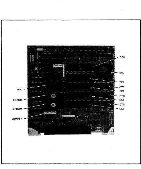
The HP 27130A Eight-Channel Multiplexer (MUX) is shown in fIgure 1-1 and consists of a printed circuit card, a cable, an RS-232-C connection box, and an installation manual.
FUNCTIONAL DESCRIPTION
The HP 27130A Eight-Channel Multiplexer provides multiplexed connections between a Hewlett-Packard computer system and up to eight EIA RS-232-C/RS-423-A/RS-422-A type devices (not including modems).
Figure 1- 2 shows a Hewlett-Packard computer system using CHANNEL I/O and the MUX. (CHANNEL I/O is a Hewlett-Packard standard defining the physical and electrical characteristics for an I/O system consisting of an I/O channel, an I/O channel adapter, and I/O cards. The MUX is one of the I/O cards.)
HP 27130A
I/O CARD
I/o CHANNEL
ADAPTER
I/O CARD
I/O
CARD
MUX
CARD
...
- - - - ,
I/O
DEVICE
o UP TO
o e
o DEVICES
I/O
DEVICE
The HP 27130A uses several of the Z-80A family of microprocessor components to relieve the host computer of much of the overhead. This permits a wide range of configurable transmission modes and formats, thus allowing connections to various CRT terminals, printing terminals, printers, and plotters.
EQUIPMENT SUPPLIED
The standard HP 27130A Eight-Channel Multiplexer consists of the following items (see figure 1-1):
Printed circuit card, part number 5061-4929
Seventy centimeter (27.5 inch) RS-232-C connection box cable, part number 8120-4076
RS-232-C connection box; part number 12828-60001
Extension cable kit, part number 12828-60004
EPROMs, part numbers 27130-80003 and 27130-80004
Installation manual, paI't number 27130-90001
IDENTIFICA TION
The Product
Up to five digits and a letter (2 7130A in this case) are used to identify Hewlett-Packard products. The five digits identify the product; the letter indicates the revision level of the product.
Printed Circuit Card
The printed circuit card supplied with the HP 27130A product is identified by a part number
marked on the card. In addition to the part number, the card is further identified by a letter and a four-digit date code (e.g., A;...230l). This designation is placed below the part number. The letter identifies the version of the etched circuit on the card. The date code (the four digits following the letter) identifies the electrical characteristics of the card with components mounted. Thus, the complete part number on the MUX card is:
HP 27130A
Manuals
The Installation Manual (part number 27130-90001, supplied with the HP 27130A product) and this manual (HP 27130 Technical Reference Manual, part number 27132-90006) are identified by name and part number. (Note that this manual is part of the HP 27132A Technical Reference Package.) The name, part number, and publication date are printed on the title page of each
manual. If the manual is revised, the publication date is changed. In this manual, the "Printing
History" page (page ii) records the reprint dates and manual update record. Reprint dates for
the Installation Manual are printed on the title page.
SPECIFICA TIONS
Table 1-1 lists the specifications of the MUX.
Table 1-1. Specifications
FEATURES
*
Eight full-duplex asynchronous serial
lID
ports
*
EIA RS-232-C/RS-423-A compatible
*
Simplex, echoplex, half-duplex, or full-duplex mode operation
*
Asynchronous baud rates from 110 baud to 19.2K baud
*
Programmable character size of 7 or 8 bits
*
1 or 2 stop bits
*
Parity: programmable even, odd, forced 1, forced 0, or none
*
Break detection
*
Parity, overrun, and framing error detection
*
Firmware based self-test
*
Optional device handshakes: host or device controlled X-ON/X-OFF, or
host controlled ENQ/ACK
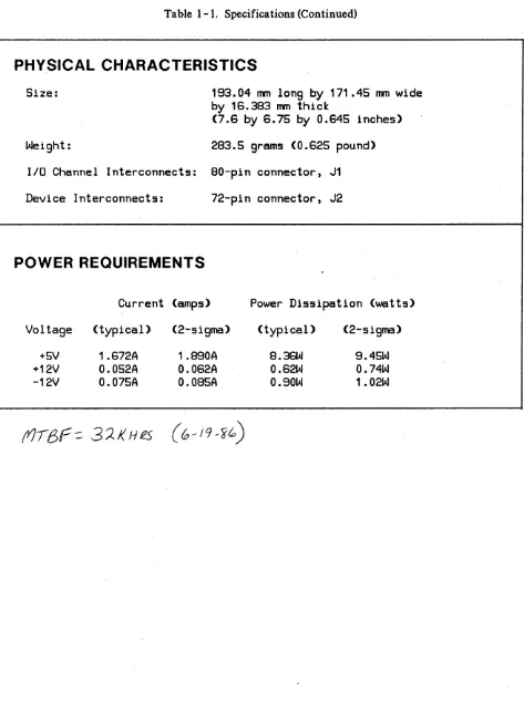
[image:11.613.57.547.82.749.2]Table 1-1. Specifications (Continued)
PHYSICAL CHARACTERISTICS
Size:
193.04 mm long by 171.45 mm wide
by· 16.383 mm thick
(7.6 by 6.75 by 0.645 inches)
Weight:
283.5 grams (0.625 pound)
lID
Channel Interconnects: 80-pin connector, J1
Device Interconnects:
72-pin connector, J2
POWER REQUIREMENTS
Current (amps)
Power Dissipation (watts)
Voltage
(typical)
(2-sigma)
(typical)
(2-sigma)
+SV
1.672A
1 .890A
8.36W
9.4SW
+12V
0.052A
O.062A
O.62W
0.74W
[image:12.612.87.560.73.718.2]INSTALLATION
1-~---~[[]
This section provides information on installing and checking the operation of the MUX.
DETERMINING CURRENT REQUIREMENTS
The MUX circuit card obtains its operating voltages from the host computer> power supply through the I/O channel. Before installing the card, it is necessary to determine whether the added curre,nt will overload the power supply. The current requirements of the card are listed in the power requirements entry of table 1-1. Current requirements for all other I/O cards can be found in the appropriate Technical Reference Manuals.
FIRMW ARE (EPROM) INST ALLA TION
I
CAUTIONI
SOME OF THE COMPONENTS USED IN THIS PRODUCT ARE SUSCEPTIBLE TO DAMAGE BY STATIC DISCHARGE. REFER TO THE SAFETY
CONSIDERATIONS INFORMATION AT THE
FRONT OF THIS MANUAL BEFORE HANDLING THE CARD OR REMOVING OR REPLACING COMPONENTS.
HP 27130A
CPU
SIC
SID
CTC MIC
SID
CTC
EPROM SID
CTC
EPROM SID
JUMPER
[image:15.613.59.551.59.650.2]Additionally, when installing or removing EPROMs, guard against bending or breaking the pins on the component. These pins also can become folded between the component and its socket, which would result in intermittent operation of the MUX. In most cases, a bent or damaged pin can be straightened with careful use of needle-nose pliers.
JUMPERS
There are two jumpers on the MUX card: a Memory Configuration jumper, and a Signature Analysis jumper. The locations of these two jumpers are shown on figure 2-1.
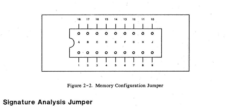
Memory Configuration Jumper
The Memory Configuration jumper, WI, is an internally-connected, IS-pin dual in-line package (DIP) shunt network. The jumper is used to configure the two memory sockets (U64 and U74) to ac-comodate different kinds of EPROMs and static RAMs. The pin diagram of WI is shown in figure
2-2, pin functions are listed in table 2-1.
18 17 18 15 14 13 12 11 10
2 3 4 5 6 7 8 9
Figure 2-2. Memory Configuration Jumper
Signature Analysis Jumper
[image:16.612.73.549.331.556.2]HP 27130A
JUMPER
A
B
C
D
E
F
G
H
J
Table 2-1. Functions of the Memory Configuration Jumper
FUNCTION
Installed only when a 16K byte EPROM is used in socket U64.
Position A connects OCE2- of the Memory Interface Circuit (MIC)
to pin 20 (CE-) of the EPROM in socket U64.
This enables the
EPROM in socket U64 whenever the lower 16K bytes of memory are.
addressed.
Installed only when a 4Kor 8K byte EPROM is used in socket U64.
Position B connects OCEO- of the MIC to pin 18 (CE-) of the 4K
byte EPROM or pin 20 (CE-) of the 8K byte EPROM,
depending on
which EPROM is installed in socket U64.
This enables the EPROM
in socket U64 whenever the lower 8K bytes of memory are
addressed.
Installed only when a 4K byte EPROM is used in socket U64.
Position C connects +5V power to pin 24 (VDD) of the 4K byte
EPROM.
Installed only when a 16K byte EPROM
is used in socket U64.
Position D connects A13 of the address bus to pin 24 (A13) of
the 16K byte EPROM.
Installed only when an 8K byte EPROM is used in socket U74.
Position E connects +5V power to pin 27 (VPP-) of the 8K byte
EPROM.
Installed only when an 8K byte static RAM is used in socket U74.
Position F connects WR- of the
Z-80~CPU to pin 27 (WE-) of the
static RAM, thus enabling the CPU to write to the RAM.
Installed only when a 2K byte static RAM is used in socket U74.
Position G connects WR- of the Z-80B CPU to pin 21 (WE-) of the
static RAM, thus enabling the CPU to write to the RAM.
Installed only when a 4K or 8K byte EPROM or an 8K byte static
RAM is used in socket U74.
Position H connects A11 of the Z-80B
CPU address bus to pin 23 (A11) of the 4K or 8K byte EPROM or 8K
byte RAM, depending on which device is installed in
~ocketU74.
1" 13 12 11 10 a
2 3 " 5 S 7
Figure 2- 3. Signature Analysis Jumper Internal Connections
1/0
CHANNEL INTERFACE
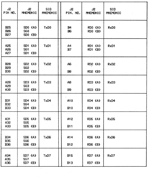
All interface between the MUX and the host computer occurs on the I/O channel. An 80-pin con-nector (J 1) located on the MUX mates with a receptacle on the I/O channel. Connections to J 1 are listed in table 2-2.
PERIPHERAL DEVICE INTERFACE
Interface between the MUX card and up to eight peripheral devices is via a 72-pin connector (J2)
to a connection panel (RS-232-C Connection Box, part number 12828-60001) and from there, via eight separate connectors and eight cables, to the peripheral devices. A connection diagram for the connection box is shown in figure 2 - 4.
Connector J2 pin assignments are shown in table 2-3. Pin assignments for J2 and the connec~
HP 27130A BALANCED RECEIVER
~
~ '-DRIVER7
HP 271JOA
MVLTlPLEXER
850 pf
FRAME GROUND II
II
RECEIVED MTA (RD-)
SEND MTA (50-0
+12'V
SIGNAL GROUND SEND COMMON (SO+)
RECEIVED OATA (RD+)
-12V
17.
,.
1
m
.
2.
:54
~
1K
35 AAAA. 6 y y y
1-111 7
1-16 8
9
lK
36 ~AA'" 10
y y y
20
R5-232-C PANEL
• 36-PIN CONNECTOR RECEIVED PINOUTS
RECEIVE CH.',NNEL PIN I SEND CHoINNEl PIN
*
RDO-JJ R04-2~ 500-34 S04-26R01-J1 RD5-23 501-32 505-24 RD2-29 RD6-21 SD2-3O 506-22 ROJ-27 R07-1~ 503-28 SD7-20
PROTECTIVE GROUND (M)
TRAN5MIlTED OATA (SA)
RECEIVED DATA (89)
REQUEST TO SEND (CA)
CLEAR TO SEND (ca)
o.t.TII SET AEADY (CC)
SIGNAL GROUND (,t,B)
CARRIER OETECT(CF)
ON (+12V)
OFF (-12\0
OATA TERt,lINAL READy (CO)
PERIPHE:I'W.
DEVICE
Table 2-2. I/O Channel Connector Jl
PIN NO.
SIGNAL MNEMONIC
SIGNAL DEFINITION
A1
RES
Not used
A2
DB14-
Data Bus, Bi t 14
A3
DB12-
Data Bus, Bit 12
A4
GND
Ground
AS
DB10-
Data Bus, Bi t 10
A6
DBB-
Data Bus, Bit 8
A7
GND
Ground
A8
DB6-
Data Bus, Bit 6
A9
DB4-
Data Bus, Bit 4
A10
GND
Ground
A11
DB2-
Data Bus, Bit
2A12
DBO-
Data Bus, Bit
0A13
GND
Ground
A14
AD2-
Address Bus, Bi t 2
A15
ADO-
Address Bus, Bit 0
A16
GND
Ground
A17
DOUT-
Data Out
A18
BPO-
Bus Primitive Bit 0
A19
CEND-
Channel End
A20
SYNC-
Synchronize
A21
GND
Ground
A22
CCLK
Corrmon Clock
A23
GND
Ground
A24
BR-
Burst Request
A25
DBYT-
Device Byte
A26
MYAD-
My
Address
A27
GND
Ground
A28
---
Not used
A29
---
Not used
A30
---
Not used
A31
RES
Not used
A32
PFW-
Power-Fail Warning
A33
PPON
Primary Power On
A34
GND
Ground
A35
AC-
Not used
A36
AC+
Not used
A37
-12-
-12V
A38
+12
+12V
A39
+5S
Not used
HP 27130A .
Table 2-2. I/O Channel Connector Jl (Continued)
PIN NO.
5 I GNAL MNEMON I C
SIGNAL DEFINITION
B1
---
Not used
B2
DB15-
Data Bus, Bit 15
B3
DB13-
Data Bus, Bit 13
B4
GND
Ground
B5
DB11-
Data Bus, Bit 11
B6
DBS-
Data Bus, Bit
9B7
GND
Ground
B8
DB7-
Data Bus, Bit 7
BS
DB5-
Data Bus, Bit 5
B10
GND
Ground
B11
DB3-
Data Bus, Bi t 3
B12
DB1-
Data Bus, Bi t 1
B13
GND
Ground
B14
AD3-
Address Bus, Bit 3
B15
AD1-
Address Bus, Bit 1
B16
GND
Ground
B17
UAD-
Unary Address
B18
BP1-
Bus Primitive Bit 1
B19
CBYT-
Channel Byte
B20
PoLL-
Poll
B21
GND
Ground
B22
10SB-
lID
Strobe
B23
GND
Ground
B24
ARQ-
Attention Request
B25
DEND-
Device End
B26
IFC-
Interface Clear
B27
GND
Ground
B28
---
Not used
B29
---
Not used
B30
RES
Not used
831
ISPU
Not used
832
NMI-
Non-Maskable Interrupt
B33
SPoN
Secondary Power On (NOT USED BY MUX CARD)
834
GND
Ground
835
AC-
Not used
836
AC+
Not used
B37
-12
-12V
838
+12
+12V
839
+55
Not used
Table 2-3. Connector J2 Pin Assignments
J2
J2
SIO
J2
J2
SIO
PIN NO.
MNEMONIC
MNEMONIC
PIN. NO.
MNEMONIC
MNEMONIC
B25
SDO CA)
TxDO
B4
RDO CA)
RxDO
B26
SGO
136RDO CB)
B27
SDO CB)
A25
SD1 CA)
TxD1
A4
RD1 CA)
RxD1
A26
SG1
B7
RD1 CB)
A27
SD1 CB)
B28
SD2 CA)
TxD2
ASRD2 CA)
RxD2
B29
SG2
B30
SD2 CB)
B8RD2 CB)
A28
SD3 CA)
TxD3
A8
RD3 CA)
RxD3
A29
SG3
A30
SD3CB)
B9RD3 CB)
B31
SD4 CA)
TxD4
A10
RD4 CA)
RxD4
B32
SG4
B33
SD4 CB)
810
RD4 (8)
A31
SD5 CA)
TxD5
A12
RD5 CA)
RxD5
A32
SG5
A33
SDS (8)
811
RDS (8)
B34
SDG CA)
TxOO
A14
ROO CA)
RxOO
B35
SGS
B36
SOO (8)
B12
ROO CB)
A34
SD7 CA)
TxD7
B15
RD7 CA)
RxD7
A35
SG7
[image:22.612.81.561.101.706.2]HP 27130A
Table 2- 3. Connector J2 Pin Assignments (Continued)
J2
J2
SIO
J2
J2
SIO
PIN NO.
MNEMONIC
MNEMONIC
PIN NO.
MNEMONIC
MNEMONIC
A17
SDO
TxDO
A21
SD4
TxD4
B17
SCO
B21
SC4
A1B
SD1
TxD1
A22
SDS
TxDS
B1B
SC1
B22
SCS
A19
5D2
TxD2
A23
500
TxOO
B19
5C2
B23
5C6
A20
5D3
TxD3
A24
5D7
TxD7
B20
5C3
B24
SC7
A3
HOOD_ON-
CT5AO-
B14
SG
----B3
HLED
----
A16
GND
----A2
-12V
----
B1
+SV
Table 2-4. RS-232-C/RS-423-A Cables
J2
J2
PANEL
PANEL
PAIR
PIN NO.
MNEMONIC
PIN NO.
MNEMONIC
COLOR
NO.
--- *
---17,18
SHIELD
------A17
SDO
34
SD (JO)
LT RED
9B17
SCO
16
SG (JO)
BLACK
9A18
SD1
32
SD (J1)
DK GREEN
10
B18
SC1
14
SG(J1)
BLACK
10
A19
SD2
30
SD (J2)
DK VIOLET
11
B19
SC2
12
SG (J2)
BLACK
11
A20
SD3
28
SD (J3)
LT BLUE
12
B20
SC3
10
SG (J3)
BLACK
12
A21
SD4
26
SD (J4)
DK BLUE
13
B21
SC4
8
SG (J4)
BLACK
13
A22
SD5
24
SD (J5)
LT VIOLET
14
B22
SC5
6
SG (J5)
BLACK
14
A23
SOO
22
SD (J6)
BROWN
15
B23
SC6
4
SG (J6)
BLACK
15
A24
SD7
20
SD (J7)
DK RED
16
B24
SC7
2
SG (J7)
BLACK
16
B4
RDO (A)
33
RD (JO)
NATURAL
1
B6
**
RDO (B)
15
SG (JO)
BLACK
1
A4
RD1 (A)
31
RD (J1)
WHITE
2
B7 **
RD1 (B)
13
SG (J1)
BLACK
2
A6
RD2 (A)
29
RD (J2)
YELLOW
3
B8
**
RD2 (B)
11
SG (J2)
BLACK
3
A8
RD3 (A)
27
RD (J3)
ORANGE
4
B9 **
RD3 (B)
9SG (J3)
BLACK
4
A10
RD4 (A)
25
RD (J4)
TAN
5
B10 **
RD4 (8)
7
SG (J4)
BLACK
5
A12
RD5 (A)
23
RD (J5)
PINK
6
B11 **
'RD5 (8)
5
SG (J5)
BLACK
6
A14
ROO (A)
21
RD (J6)
GRAY
7
B12 **
ROO (B)
3
SG (J6)
BLACK
7
B15
RD7 (A)
19
RD (J7)
LT GREEN
8
HP 27130A
Table 2-4. RS-232-C/RS-423-A Cables (Continued)
J2
J2
PANEL
PANEL
PAIR
PIN NO.
MNEMONIC
PIN NO.
MNEMONIC
COLOR
NO.
B14
**
SG
--
---
---
--B2
+12V
35ON
DK RED
1
(SINGLE)
A2
-12V
36OFF
DK BLUE
2
(SINGLE)
*
- Shield connected to chassis ground through a decoupling
capacitor in J2 connector hood.
**
- These signals bused together at connector J2.
INST ALLA TION
I
CAUTIONI
ALWAYS ENSURE THAT THE POWER TO THE COMPUTER IS OFF BEFORE INSER TING OR REMOVING THE MUX CIRCUIT CARD AND CABLE. FAILURE TO DO SO MAY RESULT IN DAMAGE TO THE MUX.
I
CAUTIONI
SOME OF THE COMPONENTS USED ON THE PRINTED CIRCUIT CARD ARE SUSCEPTIBLE TO DAMAGE BY STATIC DISCHARGE. REFER TO THE SAFETY CONSIDERATIONS INFORMATION AT
THE FRONT OF THIS MANUAL BEFORE
HANDLING THE CARD.
Install the MUX as follows:
2. Verify that the Memory Configuration jumper is configured correctly for the EPROMs/RAMs installed on the card. To verify that the jumper is configured correctly, determine what types of EPROMs/RAMs are installed in sockets U64 and U74, then refer to table 2-1 to verify that the correct jumpers are closed.
3. Install the card in the appropriate slot in the computer. Refer to the computer system in-stallation manual to determine the correct slot. When installing the card, use c,are not to damage components or traces on the card or on adjacent cards. Press the MUX card firmly into place.
4. Connect the cable supplied with the card from J2 to the RS-232-C connection box. If you
have the test hood, which exercises more of the card's circuitry, and can be ordered (Hewlett-Packard part number 0950-1659), connect it to J2 instead of connecting the cable.
START-UP
I
CAUTIONI
BE SURE AND INSTALL THE DIAGNOSTIC TEST HOOD SO THAT ITS COMPONENT SIDE (THE SIDE WITH THE LED) MATCHES THE COMPONENT SIDE ON THE MUX CARD. DAMAGE TO THE MUX CARD CAN RESULT IF THE COMPONENT SIDES OF THE TWO DEVICES DO NOT MATCH.
To start up and verify correct operation of the MUX, perform the following:
1. Turn on computer system power.
2. A self -test is contained on the card. The host computer system determines if the self -test is run automatically at power-on or must be invoked by the user. Refer to the appropriate manual for your system for a description of self -test initiation.
a. If the diagnostic test hood is not installed when the self -test executes, the LED located on the
card should light briefly and go out. This indicates that the card passed self-test. If the LED
does not light at all, the card is defective. If the LED stays on, the card did not pass
self-test. For either of these latter two cases, it is recommended that you return the card
to Hewlett-Packard; refer to the next paragraph for reshipment information. If you wish to
perform maintenance on the card, however, refer to Sections V, VI, and VII for maintenance in-formation, replaceable parts lists, and schematic logic diagrams, respectively.
b. If the diagnostic test hood is installed wh~n the self-test executes, the conditions in step 2.a.
should occur, plus the LED located on the test hood should light briefly and go out. If the
LEOs (the one moun~ed on the card and the one on the diagnostic test hood) do not light at all,
HP 27130A
RESHIPMENT
If the MUX is to be shipped to Hewlett-Packard for any reason, attach a tag identifying the
owner and indicating the reason for shipment. Include the part number of the MUX.
Pack the card in the original factory packing material, if available. If the original material is not
PRINCIPLES OF OPERA TION
1-~---~~
FUNCTIONAL DESCRIPTION
A functional block diagram of the HP 27130 Eight-Channel Multiplexer is shown in figure 3-1. Reference will also be made to the schematic logic diagram contained in Section VII, figure 7-1.
Note that figure 7-1 consists of five sheets. References to this figure will be as follows: All, 7-1;
C23, 7-1; D37, 7-1, etc., where the first digit (1, 2, 3, 4, or 5) refers to the sheet number; the
com-bination of letters A through E and numbers 11 through 58 (All, D37, etc.) refer to the quadrants on the individual sheets; and 7-1 refers to the figure number. For example,
r
quadrantA11
L
sheet 1r
quadrantD37
L
sheet 3Circuitry contained on the MUX card includes a Backplane Interface Circuit (BIC) gate array and its support circuits, a Z-SOB microprocessor (CPU), three Z-80 Counter Timer Circuits (CTCs), four Z- 80 Serial I/O circuits (SI0/2s), up to 16K bytes of EPROM in two 28-pin sockets, a Memory
Interface Circuit (MIC) gate array, 64K bytes of dynamic RAM (48K available)
RS-422-A/RS-423-A transmitters and receivers (compatible with RS-232-C and CCITT V.2S), and I/O channel (backplane) and peripheral device panel (frontplane) connectors.
The heart of the MUX card is the Z-SOB CPU (U33, see D24, 7-1), which through a program stored in EPROM controls the functions of the card.
The Backplane Interface Circuit (BIC, U41, see A14, 7-1) is a custom gate array integrated circuit which controls the communication and handshaking with the I/O channel (backplane). The BIC is accessed by the Z-SOB CPU as an I/O device for control information, and through Direct Memory Access (DMA) for data transfer to memory.
The Counter Timer Circuits (CTC, U51, U61, and U71, see E43, 7-1) divide the system clock to provide baud rate clocks and other necessary clocks for the MUX. They are accessed by the Z-80B CPU as I/O devices.
HP 27130A
~
~ SERIAL LA.!
I/O
Q 0 LA.!
~
0::a. DATA
~
,....
· 0
8 IAJ
~
S
-
..J ~ a:: /l.~ 0 ~
z ~ ~
~
~ II..0 AIlOR '-" C'4
g
16 ""J....
..,
Z-80B
<:PU SERIAL
I/o
System Clocks
Three synchronized system clocks (1.8432 MHz, 3.6864 MHz, and 7.3728 MHz), all derived from
the I 4.7456 MHz clock signal CCLK + (see A 21, 7 -1), perform the following functions:
1.8432 MHZ (PHI_CTC): Provides input to the CLK/TRGpins on the CTCs to generate _ baud rates and system timing intervals.
3.6864 MHz (PHI): Used to provide a system clock to the Z-80B CPU, the SIOs and MIC,
and the CTCs.
7.3728 MHz (2_PHI): Drives the MIC.
Memory Address Space
The Z-80B CPU address space of 64K bytes is divided into several sections as shown in figure 3-2.
The two memory sockets, U64 and U74, are reserved for EPROMs and/or static RAMs. Socket U64 can be configured for 4K, 8K, or 16K byte EPROMs. Socket U74 can be configured for 4K byte EPROM, 8K byte EPROM, 2K byte static RAM, or 8K byte static RAM. Note, however, that when a
16K byte EPROM is installed in U64, socket U74 must be left empty to avoid bus contention.
The address space of U64 is from OH to 3FFFH when this socket is configured for the 16K byte EPROM. The address space is from OH to IFFFH when the socket is configured for 4K or 8K byte EPROMs.
The address space of U74 is fixed between 2000H to 3FFFH.
The following types of EPROMs can be installed in socket U64:
4K by 8 (Intel 2732) 8K by 8 (Intel 2764) 16K by 8 (Intel 27128)
The following types of EPROMs and static RAMs can be installed in socket U74:
4K by 8 EPROM (Intel 2732) 8K by 8 EPROM (Intel 2764)
2K by 8 static RAM (Hitachi HM-6116) 8K by 8 static RAM (HitachiHM-6164)
Memory Configuration jumper WI is used to configure the two memory sockets. WI contains
nine jumper positions: A, B, C, D, E, F, G, H, and J. Positions A through D configure socket U64;
positions E through H configure U74; and position J enables the WAIT- signal of the MIC to the
Z-80B
cpu.
The MIC always asserts the WAIT- signal when the lowest 16K byte address isac-cessed. Position J should be closed (a jumper installed) when EPROMs/RAMs with access times
HP 27130A
The 4K by 8 EPROMs and 2K by 8 static RAMs are 24-pin packages and are installed to the back of the sockets (pins 1, 2, 27, and 28 are not used).
Tables 3-1 and 3-2 show the settings of WI for different types of EPROMs/RAMs.
64K
FFFFH
I -
-
DFFFH
48K
-
64K-
8FFFH
DYNAMIC RAM
-
-
9FFFH
(48K USED)
32K
-
-
7FFFH
-
-
5FFFH
16K
3FFFH
4K. 8K EPROM
8K 2K. 8K STATIC RAM
1FFFH
4K. 8K EPROMOOOOH
MEMORY MAp·
Table 3-1. Memory Configuration Jumper (W 1) Settings for Socket U64
SETTINGS
ADDRESS
SOCKET
SPACE
AB
C
D
U64
COttMENTS
OOOOH-
OPEN
CLOSED
CLOSED
OPEN
4K x 8
OFFFH
Intel
(4K)
2732
OOOOH-
OPEN
CLOSED
DON'T
OPEN
8K x 8
1FFFH
CARE
Intel
(8K)
2764
OOOOH
CLOSED
OPEN
OPEN
CLOSED
16K x 8
Socket
3FFFH
Intel
U74 mU!5t
(16K)
27128
be empty
Table 3-2. Memory Configuration Jumper (W 1) Settings for Socket U74
SETTINGS
ADDRESS
SOCKET
SPACE
E
F
G
HU74
COttMENTS
2000H
DON'T
OPEN
OPEN
CLOSED
4K x 8
4K byte
2FFFH
CARE
Intel
EPROM
(4K)
configuration
2000H
CLOSED
OPEN
OPEN
CLOSED
8K x 8
8K byte
3FFFH
Intel
EPROM
(8K)
2764
configuration
2000H
OPEN
CLOSED
CLOSED
OPEN
2K x 8
2K byte
27FFH
Hitachi
static RAM
HP 27130A
1/0
Address Space
The Z-80B CPU provides addressing capability for 256 distinct I/O port registers. The MUX card uses only 47 I/O port register addresses: 16 are reserved for the four Z-80 SIOs, 12 are reserved for the three Z- 80 CTCs, 12 are reserved for the MIC, and seven are reserved for the BIe.
Table 3-3 shows the I/O addresses used by the card.
I
CAUTION
I
THE USE OF ANY OTHER ADDRESSES MAY CAUSE IMPROPER OPERATION.
Z-808
Microprocessor CPU
The Z-80B CPU (U33) is an MOS LSI microprocessor which operates from a single +5-volt supply, uses a single-phase clock, and has a typical instruction execution time of I microsecond. The data bus is eight bits wide, and the address bus is 16 bits wide. All CPU pins are TTL compatible.
The Z-80B CPU employs a register-based architecture which includes two sets of six general-purpose registers which can be used as individual 8-bit registers or 16-bit register pairs. Additional 8-bit registers include two sets of accumulator and flag registers, and the interrupt vector and memory refresh registers. Additional 16-bit registers include the stack pointer, program counter, and two index registers. The Z-80B CPU provides the intelligence for the MUX card to function as a preprocessor for the I/O devices, thus relieving the host computer of a considerable amount of processing.
The functions of the Z- 80B CPU signals are shown in table 3-4.
Z
-80
S10/2 (Serial 1/0 Controller)
The MUX card uses four Z-80 S10/2 controller circuits (U43, U53, U63, and U73, see A42, . 7 -1). The Z -80 SI 0 /2 is a programmable serial 1/ 0 controller with two independent full-duplex channels, each of which contains separate control and status lines. Each channel can be indepen-dently programmed. On the MUX card, each of the eight channels is used as a fully programmable asynchronous terminal controller.
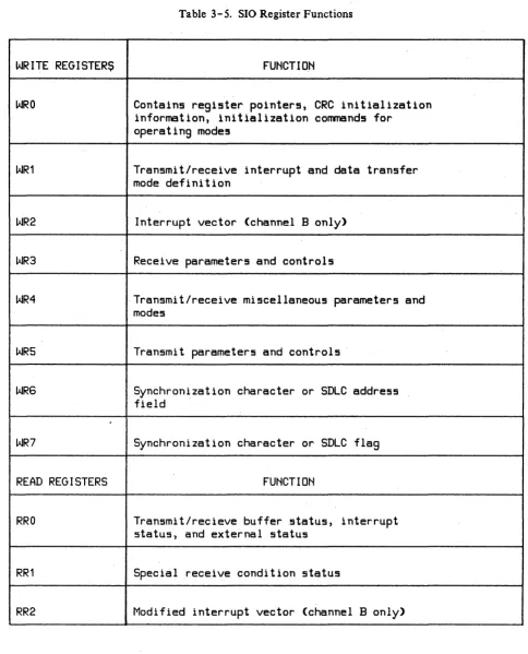
Each SIO channel has two I/O addressable ports: one port for data transfer, and one for control in-formation. Each control port has three read registers and eight write registers available for con-trol information. The functions performed by the registers are shown in table 3-5.
Table 3-3. I/O Address Space
lID
ADDRESS LINES
lID
PORT
lID
PORT FUNCTION
7
6
54
3
21
0ADDR
MIC Regi5ter 0
1 11
0 00
0 0EO H
MIC Regi5ter
11
11
0 00
01
E1 H
MIC Regi5ter
2 11
1
0 00
1
0E2 H
MIC Regi5ter 3
11
1
0 00
1
1
E3 H
MIC Regi5ter 4
11
1
0 0 1 0 0E4 H
MIC Regi5ter
51
1
1
0 01
01
E5 H
MIC Regi5ter 6
1
11
0 01
1
0E6 H
MIC Regi5ter 7
1
1
1
0 01
1
1
E7 H
MIC Regi5ter 8
11
1
01
0
0 0E8 H
MIC Regi5ter 9
11
1
01
0
01
E9 H
MIC Regi5ter 10
11
1
0
1
0
1
0EA H
MIC Regi5ter 11
1
1
1
0
1
0
1
1
EB H
CTC 0:
Channel
01
1
0
1
0
00
0DO H
CTC 0:
Channel 1
1
1
01
0
0 01
D1 H
CTCO:
Channel 2
11
01
0
01
0D2 H
CTC 0:
Channel 3
11
01
00
1
1
D3 H
CTC 1: Channel
0 1 10
1
01
0
0D4 H
CTC 1: Channel 1
11
0
1
0
1
01
D5 H
CTC 1: Channel 2
1 10
1
0
11
0
OOH
CTC 1: Channel 3
1 10
1
01
1
1
D7 H
CTC 2: Channel 0
11
01
1
00
0
D8H
CTC 2: Channel 1
11
0
1
1
0
0
1
D9H
CTC 2: Channel 2
11
0
1
1
0
1
0DA H
CTC 2:
Channel 3
1
1
0
1
1
0
1
1
DB H
BIC Regi5ter 0
1
0
1
1
X
0
0 0BO H
BIC Regi5ter 1
1
0
1
1
X
0
0
1B1 H
BIC Regi5ter 2
10
1
1
X
0
1
0B2 H
BIC Regi5ter 3
10
1 1X
0 1 1B3 H
BIC Regi5ter 4
1
0 11
X
1
0
0B4 H
BIC Regi5ter
5 1 0 11
X
10
1
B5 H
BIC Regi5ter 6
10
1
1
X
1
1
0
B6H
BIC Regi5ter 7
1 01
1
X
1
1
1
B7 H
HP 27130A
Table 3-3. I/O Address Space (Continued)
110 ADDRESS LINES
110
PORT
110 PORT FUNCTION
7
6
5
4
3
2
1
0
ADDR
SID 0: Channel A Data
0
1
1
1
0
0
0
0
70 H
SID 0: Channel A Control
0
1
1
1
0
0
0
171 H
SID 0: Channel B Data
0
1
1
1
0
0
1
0
72 H
SID 0: Channel B Control
0
1
1
1
0
0
1
1
73 H
SID 1: Channel A Data
0
1
1
1
0
1
0
0
74 H
SID 1: Channel A Control
0
1
1
1
0
1
0
1
75 H
SID 1: Channel B Data
0
1
1
1
0
1
1
0
76 H
SID 1: Channel B Control
0
1
1
1
0
1
1
1
77 H
SID 2: Channel A Data
0
1
1
1
1
0
0
0
78 H
SID 2: Channel A Control
0
1
1
1
1
0
0
1
79 H
SID 2: Channel B Data
0
1
1
1
1
0
1
0
7A H
SID 2: Channel B Control
0
1
1
1
1
0
1
1
7B H
SID 3: Channel A Data
0
1
1
1
1
1
0
0
7C H
SID 3: Channel A Control
01
1
1 1 1 0 17D H
SID 3: Channel B Data
0
1
1
1
1
1
1
0
7E H
SIGNAL NAME
AO - A15
(Address Bus)
DO - D7
(Data Bus)
M1-(Machine Cycle
1)MREQ-(Memory Request)
10RQ-(Input/Output
Request)
Table 3-4. Z-80B CPU Signals
FUNCTION
Tri-state output, active high.
AO - A15 are a 16-bit address bus (AO is the
least significant bit). This bus provides
address capability for up to 64K of memory data
exchanges, and for I/O device data exchanges.
I/O addressing uses the a lower address bit5
to allow direct addressing of up to 256 input
or 256 output ports.
Tri-state input/output, active high.
DO - D7
are an a-bit bidirectional data bus
used for data exchanges with memory and I/O
devices.
Output, active low.
Indicates that the current machine cycle is
the OP code fetch cycle of an instruction
execution.
Tri-state output, active low.
Indicates that the address bus holds a valid
address for a memory read or write.
Tri-state output, active low.
Indicates that the lower half of the address
bus holds a valid I/O address for an I/O read
or write.
10RQ- is also generated with
HP 27130A
SIGNAL NAME
RD-(Read)
WR-(Write)
RFSH-(Refresh)
HALT-
WAIT-
INT-(Interrupt
Request)
NMI-(Non-Maskable
Interrupt)
Table 3-4. Z-80B CPU Signals (Continued)
FUNCTION
Tri-state output, active low.
Indicates that the CPU wants to read data
from memory or an
lID
device. Memory or
lID
device uses this signal to gate data onto
the CPU data bus.
Tri-state output, active low.
Indicates that the CPU data bus holds valid
data for the addressed memory or
lID
device.
Not used by the MUX card.
Not used by the MUX card.
Input, active low.
Indicates to the Z-808 CPU that the addressed
memory or
lID
devices are not ready for a
data transfer. This signal allows memory
or
lID
devices of any speed to be
synchronized to the Z-808 CPU.
Input, active low.
Generated by
liD
devices. A request will be
honored at the end of the current instruction
if an internal Interrupt Enable flip-flop
is enabled and if the BUSRQ- signal is not
active.
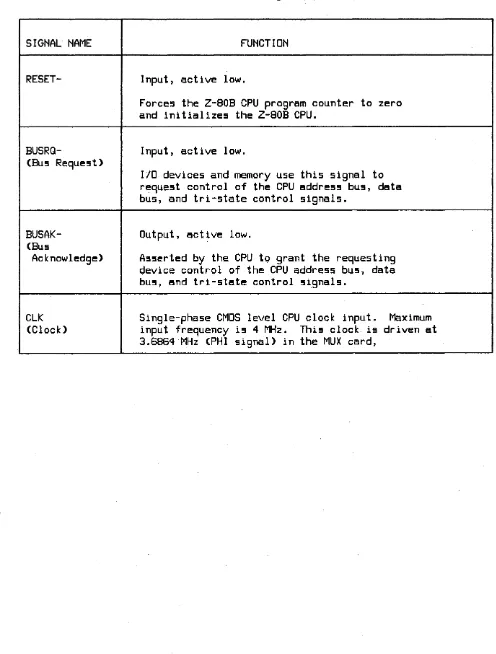
[image:37.613.54.551.91.709.2]SIGNAL NAME
RESET-
BUSRQ-(Bus Request)
BUSAK-(Bus
Acknowledge)
ClK
(Clock)
Table 3-4. Z-80B CPU Signals (Continued)
FUNCTION
Input, active low.
Forces the Z-80B CPU program counter to zero
and initializes the Z-80B CPU.
Input, active low.
110 devices and memory use this signal to
request control of the CPU address bus, data
bus, and tri-state control signals.
Output, active low.
Asserted by the CPU to grant the requesting
device control of the CPU address bus, data
bus, and tri-state control signals.
Single-phase CMOS level CPU clock input. Maximum
input frequency is 4 MHz.
This clock is driven at
[image:38.615.62.558.91.745.2]HP 27l30A
Table 3- 5. SIO Register Functions
WRITEREGISTER$
FUNCTION
WRO
Contains register pOinters, CRC initialization
information, initialization conmands for
operating mode9
WR1
Transmit/receive interrupt and data transfer
mode definition
WR2
Interrupt vector {channel B only>
WR3
Receive parameters and controls
WR4
. Transmit/receive miscellaneous parameters and
modes
WR5
Transmit parameters and controls
WR6
Synchronization character or SDLC address
field
WR7
Synchronization character or SDLC flag
READ REGISTERS
FUNCTION
RRO
Transmit/recieve buffer status, interrupt
status, and external status
RR1
Special receive condition status
[image:39.613.68.552.79.678.2]SID
SID
NO.
MNEMONIC
o
RTSA-(OUTPUT)
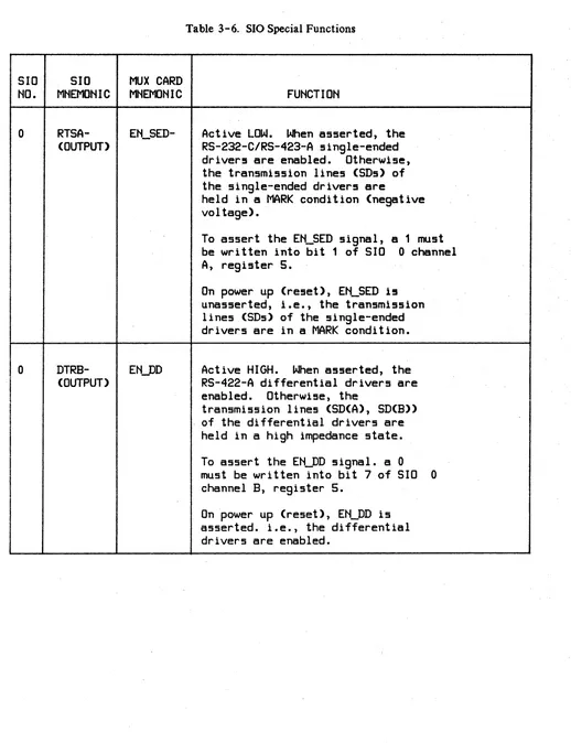
Table 3-6. SIO Special Functions
MUX CARD
MNEMONIC
FUNCTION
EN_SED-
Active LOW.
When asserted, the
RS-232-C/RS-423-A single-ended
drivers are enabled. Otherwise,
the transmission lines (SDs) of
the single-ended drivers are
held in a MARK condition (negative
vol tage).
To assert the EN_SED signal, a 1 must
be written into bit 1 of SID 0 channel
A, register 5.
On power up (reset), EN_SED is
unasserted, i.e., the transmission
lines (SDs) of the single-ended
drivers are in a MARK condition.
o
DTRB-
EN_DD
Active HIGH.
When asserted, the
RS-422-A differential drivers are
enabled. OtherWise, the
transmission lines (SD(A), SD(B»
of the differential drivers are
held in a high impedance state.
(OUTPUT)
To assert the EN_DD signal. a 0
must be written into bit 7 of SID 0
channel B, register 5.
[image:40.612.70.588.54.728.2]HP 27130A
Table 3-6. SIO Special Functions (Continued)
o
SIO
SID
MUX CARD
NO.
MNEMONIC MNEMONIC
1
o
RTSB-(OUTPUT)
RTSB-(OUTPUT)
DTRA-(OUTPUT>
LED
LOOP-FUNCTION
Active HIGH. When asserted, the
MUX card LED is turned on.
To assert the LED signal, a 0 must
be written into bit
1of SID
0channel B, register
5and SID
1channel B, register
5.
On power up (reset), LED is asserted,
i.e., the LED on the MUX card is on.
Because a minimum of 6 rnA is needed to
turn on the LED, a
422ohm resistor is
used to supply the current. Two SID
modem control signals are used in parallel
to shunt the current and turn off LED.
The control circuit of the LED is shown
in figure 3-3.
In order to avoid a large current being
sunk by only one of the two SID
control signals for a long period of time,
thus damaging one of the SIOs, the time
between programming the two SID signals
should be kept as short as possible.
Active LOW.
Whe~asserted, the
self-test loop-back circuits are
activated. The output of
TXDs (transmit data> of each SID
is fed back to the input of RXDs
(receive data) of the same channel,
e.g., the data is sent from TXDA to
RXDA of the same SID.
All eight channels are controlled by
one loop-back circuit, therefore, it
[image:41.615.73.546.64.727.2]SID
NO.
SID
MNEMONIC
CTSA-(INPUT)
Table 3-6. SIO Special Functions (Continued)
MUX CARD
MNEMONIC
FUNCTION
Both the single-ended and differential
drivers should be disabled during the
internal loop back test. This will avoid
unintentional data transmission to the
other systems through the frontplane
drivers, thus cau5ing unpredictable results.
During the internal loop-back test, all
the receivers are automatically disabled.
Thus, the card is completely isolated from
the front plane receivers.
To assert the LOOP Signal, a 1 must be
written into bit 7 of SIO 0 channel A,
register 5.
On power up (reset) LOOP- is
unasserted, i.e., no loop back.
HOOD_ON-
If the diagnostic hood is not installed,
the HOOD_ON- signal is pulled to
+5Vby a
3.3K ohm resistor on the MUX card.
If the diagnostic hood is installed, the
state of HOOD_ON- is the complement of the
state of the HLED- signal (i.e., 0-->1,
1--)0,
HLED- --) HOOD-ON-).
Figure 3-4 shows the circuit used to sense
the diagnostic hood.
This circuit is also used
to turn the hood LED on and off.
The state of the HOOD_ON- signal can be read from
bit
5of SID 0 channel 1, register O.
A 0
indicates that HOOD_ON- is being pulled to
+5V.A 1 indicates that HOOD_ON- is being pulled to
ground.
[image:42.613.44.563.76.747.2]HP 27130A
Table 3-6. SIO Special Functions (Continued)
SID
SID
MUX CARD
MNEMONIC
NO .
MNEMON I C
o
RDYA-
IJI1A2-(OUTPUT)
o
RDYB-
IJI1AO-(OUTPUT)
FUNCTION
On power up (reset), if the diagnostic hood i5
installed, the HOOD_ON- signal will be pulled to
ground.
If the diagnostic hood is not installed,
the HOOD_ON- signal will be pulled to
+5V.Active LOW.
DMA2- is tied to the
IRG2- input of the MIC.
When
is programned as
RDYA-(READY-), it isa DMA handshake
Signal. To the MIC's DMA
controller, DMA2- indicates that
channel A of SID 0 is ready to
transfer data to or from memory.
By
using the MIC's DMA capability,
channel A of SID 0 (channel 0 of
the MUX card) can support very high
data rates.
On power up (reset) DMAO- is floating.
Active LOW.
DMAO- is tied to the
IRQO- input of the MIC.
When
is programned as
RDYB-(READY-), it is a DMA handshake
Signal. To the MIC's DMA
controller, DMAO- indicates that
channel B of SID 0 is ready to
transfer data to or from memory.
By
using the MIC's DMA capability,
channel B of SID 0 (channel 1 of
the MUX card) can support very high
data rates.
[image:43.612.70.546.94.731.2]Table 3-6. SIO Special Functions (Continued)
SIO
SIO
MUX CARD
NO.
MNEMONIC
MNEMONIC
FUNCTION
1
DTRB-
HLED-
Active LOW.
When a55erted) the LED on
(OUTPUT)
the diagnostic hood i5 on.
To assert the HLED- signal) a 1 must be
be written into bit 7 of SIO 1 channel B)
regi5ter 5.
On power up (reset») HLED- is unasserted, i . e: ,
the LED on the diagnostic hood is off.
No modem control lines or modem status inputs are used.
SIO /10
422
RTSB-
-
-'IfIN---o +5VLED
SIO 61
RSTB-\/
ON-BOARD LED [image:44.615.65.562.88.672.2]HP 27130A
SIO
11
DTRB-MUX CARD
DIAGNOSTIC HOOD
HLED-S05
HLED
220
SIO
10
CTSA-3.3K
HOOD_ON---.JVVVI---O +5V
HOOD LEO
220
""---'W-/"---O GND
Figure 3-4. Diagnostic Hood LED Control Circuit and Hood Sense Circuit
[image:45.615.84.543.44.532.2]CTC (Counter Timer Circuit)
Three Z-SO CTC circuits (U51, U61, U71, see E43, 7-1) are used by the MUX card to provide baud rate and real-time clocks.
The Z- SO CTC circuit provides four independent counter/timer channels. Three of these timers can supply outputs for other devices; the fourth channel can only cause an interrupt to the Z-SOB
cpu.
Only the first CTC (CTC 0, U 51) is tied to the MUX card's daisy-chain interrupt structure and is able to generate an interrupt to the Z-SOB CPU. The fourth timer of CTC 0 is the real-time clock for the card's firmware.
CTC 1 (U61) and CTC 2 (U71) are not tied to the interrupt daisy chain, and they are not allowed to generate interrupts. These two CTCs are only used to generate baud rates.
The reason for eliminating CTC 1 and CTC 2 from the daisy-chain interrupt structure is to con-form to the timing requirements of the Z-SOB CPU during lACK and RETI cycles. See the "Wait State Circuit for Interrupt Acknowledge" paragraph for a timing analysis of the lACK and RETI cycles.
The inputs of all four clock triggers (CLK/TRGO through CLK/TRG 3) of all three CTCs are driven by the I.S432 MHz clock (PHI_CTC clock, generated by U24, see A22, 7-1).
The functions of the CTC timer outputs are shown in table 3-7.
Note that the CTCs are I/O addressable ports to the Z-SOB CPU; their addresses are defined in table 3-3.
Interfacing to the BIC
The Backplane Interface Circuit (BIC, see A 14, 7-1) provides the half -duplex data path to the I/O channel (backplane). As used by the MUX card, the BIC is addressed as an I/O port by the Z-SOB
cpu
(the same as the Z-SO SIO and CTC circuits). In other words, to read or write from the BICregisters, an IN or OUT instruction is executed to the I/O address of that register. The address space of the BIC is described in table 3- 3.
Data can also be transferred between the BIC and memory directly under control of DMA chan-nel B of the Memory Interface Circuit (MIC).
The BIC is not directly connected to the interrupt daisy chain structure of the MUX card. Instead, the BIC's BINT- (interrupt output, see E14, 7-1) signal is connected to the MIC's IINT- (in-terrupt input, see C31,7-1) signal. When the MIC is programmed for external in(in-terrupt (from the BIC), the MIC will generate an interrupt for the BIC. The MIC also provides an interrupt vector for the BIC when the Z-SOB CPU acknowledges.
HP 27130A
Table 3-7. CTC Timer Outputs
TIMER
DRIVEN DEVICE
CTC
CTC
OUTPUT
INPUT
NO.
CH.
MNEMONIC
MNEMONIC
FUNCTION
0
0
. IRQH
IRQH of MIC
Request hold-off for DMA
0
1
BRG1
SID 0
MUX card channel 1
baud-RXCB- & TXCB-
rate clock
0
2
BRGO
SID 0
MUX card channel
o
baud-RXCA- & TXCA-
rate clock
0
3
INTERNAL
Cause zero
Real-time clock for
count interrupt firmware
to Z-80B CPU
1
0
BRG2
SID 1
MUX card channel 2
baud-RXCA- & TXCA-
rate clock
1
1
BRG3
SID 1
MUX card channel 3
baud-RXCB- & TXCB-
rate clock
1
2
BRG4
SID 2
MUX card channel 4
baud-RXCA- & TXCA-
rate clock
1
3Not avai lable
Counter value can be
read <polled)
byZ-80B
[image:47.612.66.545.58.734.2]Table 3-7. CTC Timer Outputs (Continued)
TIMER
DRIVEN DEVICE
CTC
CTC
OUTPUT
INPUT
NO.
CH.
MNEMONIC
MNEMONIC
FUNCTION
2
0
BRGS
SID 2
MUX card