[Wi@
<Q]~@l@!!W
)
box 6528 denver, colorado 80206 (303) 777-7133
.
DOUBLE DENSITY
INSTALLATION MANUAL
TABLE OF CONTENTS
SECTION
PAGE
Chapter 1
Section 1 Circuit Modifications ... 1
Section 2 CPU Modifications ... .' ... 1
Section 3 Installing the CPU Modifications ... 2
Section 4 Motherboard Modifications ... 2
Chapter 2
-+)
~~::~~ ~ ~~!~I~~~ ~:~:~~·:::~t;:;7.h·::::::::::::::::::::::::::::::::::::::::::::::::::.:::::::::::::::::::::::::::::::::::::::::::::::::::J ~
Chapter 3
Section 1 Power Supply Adjustment ... 18' 17
CHAPTER 1 - Section 1
CIRCUIT MODIFICATIONS
The Double Density Controller Installation Manual contains all information regarding installation of The Digital Group Double Density Disk Controller Board into a system. Included is all CPU modifications, motherboard modifications, and cabling procedures for different systems. Included is a section regarding power supply adjustment for assembled board purchasers.
CHAPTER 1 - Section 2
CPU MODIFICATIONS
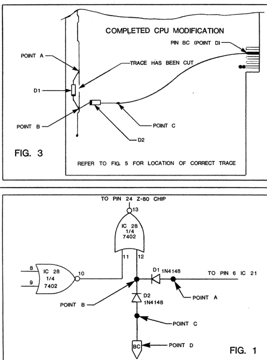
The installation of The Digital Group Double Density Controller Board requires slight modification to the Z80 CPU Board. During data transfer to and from the disk drive, the CPU must be placed in a series of wait states until data is ready. Our present Z80 CPU board (rev. C and earlier), provides only for the ROM to cause wait state generation. To correct this problem, a diode OR circuit will be added to the Z80 CPU wait line. This ORed wait line will be connected to pin BC of the Z80 CPU 100-pin edge connector.
There also is a modification to insure that the Z80 CPU is held in reset until every other board in the system has powered up. This modification requires a resistor change on the Z80 CPU board along with a diode installation. The resistor increases the RC time constant of reset, while the diode allows for quick discharge of the capacitor during power on-off-on conditions. One other modification should be mentioned here. This is the moving of the front panel reset button from reset to NMI. This modification is required for systems containing dynamic memory. The user who has static memory and intends to use only static memory need not perform this modification.
The Jast modification to be installed is the running of a wire from the CPU interrupt socket to a spare pin on the CPU 100-pin edge connector.
-1-CHAPTER 1 - Section 3
Installing the CPU Modifications
The user should first check to see if the following modifications have been made to his system. Refer to Figures 1 through 4 and perform the following (to Rev. C and earlier zao CPU boards):
1. Identify pin BC on the circuit side of the Z80 CPU card. (4th from end) 2. Cut one trace connecting IC21 pin 6 and IC28 pin 12. See Figure 2 and 3.
(A) Locate the trace on the circuit side of the zao CPU card matching Figure 2.
(B) Cut the trace between points A and B with a sharp tool like an exacto knife or razor blade.
3. Solder 01 (lN4148) across paints A and B. The banded end of the diode should be connected to point B.
4. Solder one end of 02 (lN4148) to point B (also the banded end), leaving the point C end of the diode unsoldered. 5. Cut a 6 inch piece of #30 wirewrap wire provided, and solder it between pin BC of the CPU edge connector and point C
end of diode D2.
6. Insulate the connection of the diode D2 and the #30 wire to insure no shorts exist. Refer to Figure 2 for the following (all Rev. CPU Boards):
1. Cut a 7114 inch piece of #30 wirewrap wire provided and jumper the following:
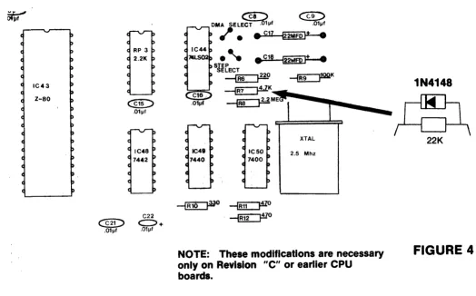
Pin a of the CPU interrupt socket and Pin C of the CPU 100-pin edge connector (3rd pin from opposite end as BC). Refer to Figure 4 for the following (for Rev. C and earlier):
1. Remove the 4 .. 7K resistor, R7 and replace it with the combination of a 22K resistor and a lN4148 diode. (A) Remove the 4.7K resistor, R7.
(B) Parallel the 22K resistor and 1 N414a diode provided.
(C) Solder this combination into R7. Orient the banded end of the diode closest to the zao IC.
CHAPTER 1 - Section 4
Motherboard Modifications
The Z80 CPU modifications added two additional pins to the zao CPU board 100-pin edge connector. To furnish these signals to The Digital Group Double Density Controller Board requires the addition of two wires on the motherboard. Please
note
that there may be a wire connecting one of these signals to the disk controller slot. Your system may also contain additional wiring for the OSS-INTl Controller, Wiring for both controllers do not conflict with each other, so the user may wish not to remove the extra wiring presently installed.Refer to Figure 5 and perform the following:
1. USing the #30 wirewrap provided, add a jumper from the zao CPU edge connector pin BC to the controller 36-pin edge connector pin 36. (This wire may already be installed.)
2. Again using the #30 wirewrap wire provided, add a jumper from the zao CPU edge connector pin C to the controller 3~ pin edge connector pin 34.
3. At the users option, remove the following wires:
(A) Z80 CPU edge connector pin 47 to controller 36-pin edge connector pin 35. (B) Controller 36-pin edge connector pin C to I/O board 36-pin edge cj)nnector pin 17.
-2-CONNECTION POINTS FOR CPU MODIFICATION
TRACE HERE
•
•
•
•
•
•
•
•
•
•
•
l
(,.)}
I
PIN BC (POINT D) "---PIN C
FIG. 2
COMPI:-ETED CPU MODIFICATION
D1--~
POINT B
FIG. 3
REFER TO FIG.
5
FOR LOCA TION OF CORRECT TRACE
TO
PIN 24 Z-80 CHIP
8
TO
PIN 6
IC
21
9
POINT
A
POINT 8
1N4148
""'---POINT 0
FIG. 1
[image:6.631.35.578.26.758.2]CPU MODIFICATIONS
C22
c:::::> +
.001Jf
NOTE: These modifications are necessary
only on Revision
"C"
or earlier CPU
boards.
JUMPERS FROM CONTROLLER CARD CONNECTOR TO CPU BUS CONNECTOR
- - - P I N 36
TANDARO 110 SLOT SELECTED PIN 34
FOR CONTROU£R CARD
---~-STANDARD 110 SLOT
~...--TVC SLOT
1N4148
22K
FIGURE 4
FIG. 5
~-CPU SLOT
NOTE:
DIAGRAM OF PIN SIDE OF MOTHERBOARD
' -_ _ _ _ --.,. _ _ _ _ _ _ _ _ _ _ _ - - - J t - - - - M E M SLOT'
[image:7.613.58.582.69.395.2]-5-CHAPTER 2 - Section 1
DSS-INT1 Cabling
The cables you have received provide a" connections for signals from the Floppy Disk Controller Card, through the backplane of the CPU cabinet, to each of the individual drives. The exact cabling arrangement is determined by the number and types of drives implemented. Figures and tables have been provided for connecting Shugart Drives.
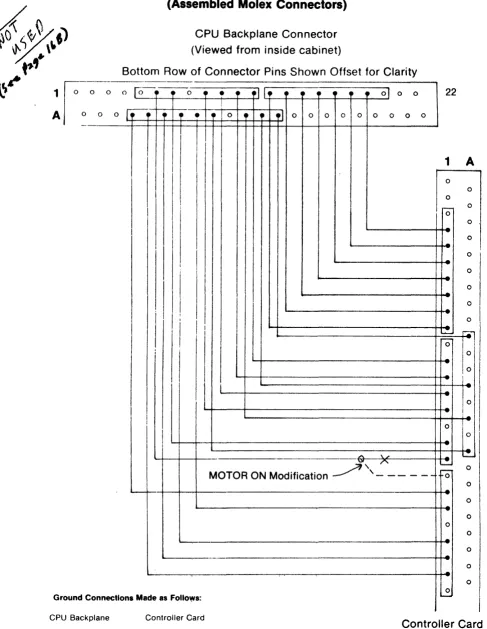
Shugart Cabling Steps
1. Using Figure 2 and Table 1, install the Molex connectors from the back of the motherboard to the CPU cabinet backplane. A 22-pi n edge connector is provided for the backplane. Note that optional 110 pins on the drive are connected to grounded pins on the CPU backplane. To use these I/O pins, remove the corresponding wire from the Molex cable. 2. Using an ohmmeter, verify a" signal connections to eliminate bad or wrong connections.
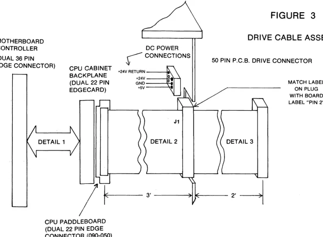
3. Connect the flat cable to the CPU backplane and the individual drives. (See Figure 3.) A Shugart PC board connector and sufficient cable are provided for each drive when you order a complete system. You must specify the number of drives in your system when ordering cable to assure getting the right number of drive connections. Be sure that the drive connector Is properly connected to the drive electronics board connector, J1. The label on drive connector pin 2 must face pin 2 on drive electronics PC board connector, J1. Reversing this cable may cause damage to the drive by applying voltage to an Incorrect pin. The CPU backplane paddlecard should be installed by thetabeling on the paddlecard. For each drive used set the device select jumper on the Shugart PC board. Jumpering is accomplished through use of a 2-position shorting plug on J1. See Figure 1.
4. In order for the drive to function properly in a multi-drive system, the last drive on the interface must have five lines terminated. As shipped from the factory, drives have jumpers on terminator posts, T1, T3, T4, T5, and T6. Remove these shorting plugs from a" drives except the last one on the interface.
S. Using a ohmmeter, verify all signal connections between the CPU backplane and the drive connector using Table 1 as a guide.
Whenever additional drives are added to your system, additional cables will be required. An upgrade kit that enables you to daisy chain from your existing cable is available. Assembly instructions for the additional cable(s) is provided with the upgrade kit.
-6-J
1
Soft-Sectored Disk Jumpering -
SHUGART
FIGURE 1
2 .
4.
b . B.
10. DC
1 2 _ .
14. 0 If) • • •
18 • • •
I • • C fl • •
S . .
[l
DDS ••
U
£:J Jumper Plug I nstalled as Shipped
• Test Point
Always installed
Installed last drive only
SA800/80l PCB Component Locations
-7-0 0
Figure 2 -
Molex Wiring Detail
(Assembled Molex Connectors)
CPU Backplane Connector
(Viewed from inside cabinet)
Bottom Row of Connector Pins Shown Offset for Clarity
--o
[0-.
•
0 4•
•
.j ,.
4•
4. 4• 4'
01 0 0!
o l~
,
,
~ -•
,
0 t • 4~I
0 0 0 0 0 0 0 0 0'I
I
I
I
I
I
I
I
I
I
I'
I
II
I
:
I
I
I
I
IA
,,,
Uf,
r.MOTOR ON Modification
~
' - - - -
--
...-.--22
1
A
0 0 0 r0- o 0 0
-
0 .-0 -. 0 0....
0-
0 ~~
~0 I
0
-
0 ]I:
--
I'-0
I
0
-
-...:..
...:..
~ 0
0 0
...
0-
0 0 0 .-0 0 .-0 0Ground Co nnectlons Made as Follo~8:
...
CPU Backplane
Pin K
Pin M
Pin N
Pin P
Controller Card
Pin U
Pin S
Pin P
Pin L
Controller Card
Note: This drayving shows the controller card
as it would be viewed through the motherboard.
(Top View)
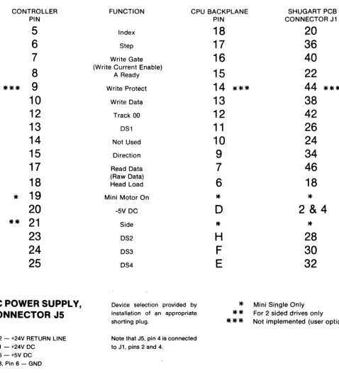
[image:10.613.50.537.76.705.2]-8-TABLE 1 -
SHUGART
CONTROLLER CARD
CPU BACKPLANE DRIVE CONNECTIONS
(See Figure 9 in. the Shugart OEM Manual
and Figure 2 in the Floppy Disk documentation)
CONTROLLER PIN
5
6
7
8
***
9
10
12
13
14
15
17
18
*
19
20
**
21
23
24
25
DC POWER SUPPLY,
CONNECTOR J5
Pin 2 - +24V RETURN LINE Pin 1 - +24V DC
Pin 5 - +5V DC Pin 3, Pin 6 - GND
FUNCTION CPU BACKPLANE SHUGART PCB
Index Step Write Gate (Write Current Enable)
A Ready Write Protect
Write Data Track 00
DS1 Not Used Direction Read Data (Raw Data) Head Load Mini Motor On
-5V DC Side DS2 DS3 DS4
Device selection provided by installation of an appropriate shorting plug.
Note that J5, pin 4 is connected to J1, pins 2 and 4.
-9-PIN CONNECTOR J1
18
20
17
36
16
40
15
22
14
***
44
***
13
38
12
42
11
26
10
24
9
34
7
46
6
18
*
*
D.
2&4
*
*
H
28
F
30
E
32
*
Mini Single Only* *
For 2 sided drives only [image:11.620.77.556.240.766.2]I
...A.
0 '
I
MOTHERBOARD
CONTROLLER
(DUAL 36 PIN
EDGE CONNECTOR)
CPU CABINET
BACKPLANE
(DUAL 22 PIN
EDGECARD)
DETAIL 1
CPU PADDLEBOARD
(DUAL 22 PIN EDGE
CONNECTOR (090-050)
DC POWER
~
CONNECTIONS
+24V RETURN - -.... \.
+24V--~.~
GND--~ +5V--~
J1
DETAIL 2
FIGURE 3
DRIVE CABLE ASSEMBLY
50 PIN P.C.B. DRIVE CONNECTOR
DETAIL 3
[image:12.794.39.700.45.530.2]FLOPPY CONTROLLER CARD 36-PIN CONNECTOR PINOUT
A GND 2 B GND 3 C GND 4 0 GND INDEX 5 E GND STEP 6 F GND WRITE GATE 7 H GND READY 8 J GND WRITE PROTECT 9 K GND WRITE DATA 10 L GND 11 M GND TRACK 00 12 N GND DS1 SELECT 13 P GND 14 R GND DIRECTION 15 S GND 16 T GND READ DATA 17 U GND • HEAD LOAD 18 VG GND MOTOR ON 19 W GND
•
-5 VDC 20 X -5 VDC SIDE SELECT 21 GND22 Z GND DS2 SELECT 23 AA GND DS3 SELECT 24 AB GND DS4 SELECT 25 AC GND
26 AD 27 AE 28 AF 29 AH 30 AJ 31 AK 32 AL 33 AM INTERRUPT (CPU) 34 AN 35 AP WAIT (CPU) 36 AR
-11-Floppy Disk Controller Card
Introduction
The Digital Group now offers all the capabilities of rapid access mass storage. With the addition of a floppy disk subsystem, the Digital Group system user can now have at his disposal 90K to 512K bytes/disk in IBM compatible format, with a worst case access time of one second.
A fully operational Digital Group floppy drive system is based on a Digital Group computer with a recommended memory size of 26K and a Z80 based processor. The complete floppy disk subsystem has a floppy disk controller card, one to four drives, power supplies for the disk drive, necessary cabling and system interconnect wiring, and cabinet(s).
System Description
The controller card is the interface between the CPU and the floppy drive(s). The controller card documentation includes a complete technical description of the controller and the controller chip, assembly instructions (including CPU card modifications), software description, listing, and tape, and diagnostic testing procedures.
To complete your floppy drive system, several additional items are required. These items are all included when ordering a complete system and may be purchased separately from The Digital Group at any time.
1. Power Supply. Each drive requires both AC and DC power sources as shown in Figure 1. AC connections foreach drive are supplied with the drive. DC connections (+24V, 24V ground, +5V, 5V ground) to each drive are provided with the Digital Group floppy power supply. Be sure all power sources are properly fused and grounded. Complete documentation is provided with each power supply ..
2. Cabling. Cables from the controller card 36-pin connector to the floppy drive(s) 22-pin connector(s) are required to transfer the proper Signals. Included in the standard Digital Group cable-pack are Molex connections from the back of the motherboard to the CPU backplane and a flat cable from the backplane to the drive(s). A different cable-pack is required depending on the number of drives in your system and an upgrade kit is available if you add drives at a later date. Complete documentation is provided for cabling your system with each cable-:pack.
3. Drives. Floppy disk drives are available in standard format from Shugart. Up to four drives may be used with the floppy controller card. Each drive includes a short AC line for connection to a power source and a complete technical manual from the drive manufacturer.
4. Cabinets that match the rest of your Digital Group system are available for single ordual drives in both standard and mini formats. Each cabinet has space for two drives and a power supply. Cabinets include AC line cord, fan, and switch, as well as assembly documentation.
-12-I
...
U)
I
I
I
I
I
I
I
I
I
I
I
FLOPPY DRIVE
~
"",
---,
POWER
I
SWITCH
I
FUSE
--L
~
-
t
= }-- -
-
II
- l . . , . / ,
,
'1111
I
~
I
~
FAN
)
:
I
~UPPUED WIT~
CABINETI _ _
I
AC AND DC WIRING DIAGRAM
FLOPPY DRIVE
In
0
0
>
0 .q- 0
0 0 C\I Z
>
Z+
~~
1.0
+
AC HARNESS
DC POWER SUPPL Y
DC
HARNESS
CHAPTER 2 - Section 2
DSM-INT1 Cabling
Installation of Termination Jumpers on the Mini-Floppy Drive
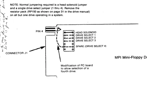
Before the drives are installed in the cabinet you need to install line termination jumpers on each drive. The jumpers required to operate in a Digital Group system are a drive select jumper and a head solenoid jumper. To use four mini-drives in a system you need to make a modification to the drive. Page 7 of the drive manual details the line termination jumpers that can be used. Figure 3 details the modification to the drive PC board and the jumpers that are used in a Digital Group system.
NOTE: Normal jumpering required is a head solenoid jumper and a single drive select jumper (1 thru 4). Remove the
resistor pack (RP150 as shown on page 31 in the drive manual) on all but one drive operating in a system.
PIN 4
~~
_---oJ
I :
I•
0 -- 0 DRIVE SELECT 1 0 HEAD SOLENOID 0 - - 0 DRIVE SELECT 2 0 - - 0 DRIVE SELECT 3I
\
\-~--~
SPARE (DRIVE SELECT 4)Modification of PC board to allow selection of a fourth drive.
[image:16.613.16.518.273.566.2]MPI Mini-Floppy Drive PC Board
FIGURE 3 -
ftIIINI-FLOPPY DRIVE JUMPERING
On Bytemaster systems a jumper wire must also be connected between the floppy controller card, pin 25, and pin 4 of the, floppy I/O connector (on the motherboard) .
On standard mainframe systems a jumper wire must be installed on the CP~ paddlecard connecting pin E (corresponding to the CPU backplane) to pin 4,
of the 34 conductor header.
-14-DRIVE CONNECTIONS FROM MINI FLOPPY POWER SUPPLY
CONNECTOR Jl ~
REAR OF DRIVE
LONGER
TO
~;I
!I \
I i !
II
..J
MPI
.,.., L
[
I
DRIVE CABLE CONNECTING
SECOND DRIVE
!
I
-r - - -
liliiii---r-Tl
CONNECTOR J2SEE P.15 IN THE MPI
DRIVE MANUAL FOR
THE CONNECTOR PINOUT
b
1
DRIVE 2Y Y Y ~ DRIVE 1
j
!
0
o
Install the 34-conductor cable in the cabinet matching pin 1 of each cable plug end to the pin 1 end of connector J1 6n each drive. Connect the paddlecard end of the cable to the CPU backplane slot designated for the mini-floppy. The backplane of the CPU is wired identically for mini-floppies as for standard floppy drives with the exception of the MOTOR ON line, pin 10. Remove Molex pin from pin 18 and move it to pin 19 of 36-pin edge connector.JUMPER ADDITION TO MINI-FLOPPY PADDLECARD
A JUMPER IS REQUIRED ON THE BACK SIDE
OF THE PADDLECARD CONNECTING PIN 4 TO PIN E
o
After installing the jumper, plug the paddleqard into the CPU backplane a!1d, using a disk operating system diskette, run the drives through reading and writing test~. Each time the drive is selec~ed the front panel LED will light, the head will load the diskette, and the drive and stepper motor will operate.-15-TABLE 1 -
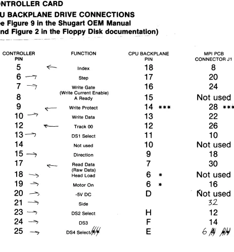
MPI
CONTROLLER CARD
CPU BACKPLANE DRIVE CONNECTIONS
(See Figure 9 in the Shugart OEM Manual
and Figure 2 in the Floppy
Di~~ doc~_men_~~t_i_!ln)
CONTROLLER PIN
5
6--=-r
7 /
8
9
10 --::;
12
13 --:;
14
15
- 7
17
18
19
20
21
23
24
25
FUNCTION~
IndexStep Write Gate (Write Current Enable)
A Ready ~ Write Protect
Write Data
~ Track 00
DS1 Select Not used Direction ~ Read Data
(Raw Data) Head Load Motor On
-5V DC Side DS2 Select
DS3
DS4select~
DC POWER SUPPLY,
CONNECTOR J2
Pin 2 - +12V Return Pin 1 - +12V DC Pin 3 - +5V DC Pin 4 - +5 Return
-16-CPU BACKPLANE PIN
18
17
16
15
14
13
12
11
10
9
7
6
6
o
H
F
E
***
*
*
MPIPCB CONNECTOR J18
20
24
Not used
28
***
22
26
10
Not used
18
30
Not used
16
Klot used
-"2 "
;:)L
12
14
6
/II
J;'
*
Modify molex on motherboard for this connection* *
Needs paddlecard & MPI PCB modification [image:18.612.86.549.106.603.2]CHAPTER 3 - Section 1
Power Supply Adjustment
The VCO Section of the Digital Group Double Density Disk Controller is referenced to the +5 Volt power supply. The free running Frequency of the
veo
is set at the f"ctory with the +5 Volt power supply setto+5.0Volts.ln order foryour controller to function properly, the user needs to adjust his +5 Volt supply. This may be Qone as follows:1. Remove the ROM from the system. 2. lnstall the controller into its intended slot.
3. Adjust the computer +5 Volt supply for;+5.0 Volts at the TOP of the contrQller board.
\
4. Reinstall the ROM previously removed.
-17-POWER CONNECTOR CONNECTIONS FOR
5k"
FLOPPY DISK DRIVE
SHUGART
&
NPI
CJMPArI~~EAMP PART NUM8ER
1-480424-0
PIN
#1 0range, +12 Volts
'2 Black, +12 Volt Return
13
Black, +5 Volt Return
14
Red, +5 Volts
AMP PAfiT NUMdER 60619-1
STRIP wIhE
1/8
INCH.
CRIMP
~TRIPPEDWIRE IN
#1.
CRIHP INSULATION IN
112.
WIRE CRIMP MAY BE SOLDERED.
INSERT INTO HOUSING FROM REAR.
CONTACT WILL SNAP IN.
o
A-I ~ I [ I2.
3
9
tf
~ ~I~
F
,!?fiji~ ,7\'~
I
iJ :
q
\
kCf
j
~
(0
I M i
II
rJ
I ,---1) 12-,
t'AACK ()O _ _ --1-4-1-1P
I (\
31
t L
;2.
I
''''/1
1
J\
NJJ
3!f
\
p
P
))"
\
SAC/{-p!,AAlt.
(f,'v,>~i:)
(2. -
5~c k~»
TOP,, _ _
(rt-, t'J ('(;;J
b?e
(f:?4b-e.
iVl v~rr-i~ (i.e ~CI
W)'v-c. t/<-1 1--:> b,o) /Y' 1JJd7
"I? ...
J
5~rr-e
/f"TV-er-t:...:j)C()IJAi
~CT1J
A(S)
TO /}ISy( IJIZI(./ IL(
c~IQ/-e
V/-e..Wed'lec..od
f~c(o-t':1 CCtn>'l'{'cT(/V )(1'\e.A-r1., )
~ I f) It. R. 0 YJ/l-TA
X
w~ plf.OTlli
,..1-N () T
E. :
C
;Jit
h-
i-{)
t?/15ts
c
~
h6
e/"1
v T' rt-
-ecI -,
f-€~ ~'T'r/~
-t7t-,4
)tJ!?~ ;J~
/T /f
(VlvcV"f-c-?"/.,) f
htf-ft-,
-e~5
(i
e.Jr1!d
Wl~~ ~~ +~j!l
t/V
tr'~ ~I
£-.v(Vc-c
t/'-t k1cJIff/V"'?
r )i I
--rltMI(
ill
·Wi(-".4TIi
""'I( Olf-
rA-f,li-P
7il(fun~N
''''(I
re)lt ()IJ.-
J,/E L j- (2).-
>~t. 2(I)
-
:, t:t. I (07/iJiiiY
5~/.T (3)
1-1 fJ ttll'i X