N A N O E X P R E S S
Open Access
Large-diameter titanium dioxide nanotube
arrays as a scattering layer for high-efficiency
dye-sensitized solar cell
Xiaolin Liu
1,2, Min Guo
2, Jianjun Cao
1, Jia Lin
1, Yuen Hong Tsang
2, Xianfeng Chen
1*and Haitao Huang
2*Abstract
Large-sized titanium dioxide (TiO2) nanotube arrays with an outer diameter of approximately 500 nm have been successfully synthesized by potentiostatic anodization at 180 V in a used electrolyte with the addition of 1.5 M lactic acid. It is found that the synthesized large-diameter TiO2nanotube array shows a superior light scattering ability, which can be used as a light scattering layer to significantly enhance the efficiency of TiO2nanoparticle-based dye-sensitized solar cells from 5.18% to 6.15%. The remarkable light scattering ability makes the large-diameter TiO2 nanotube array a promising candidate for light management in dye-sensitized solar cells (DSSCs).
Keywords:Large-diameter titanium dioxide nanotubes; Scattering layer; Dye-sensitized solar cells; Electrochemical reactions
Background
Dye-sensitized solar cells (DSSCs) have received consid-erable interest since 1991 [1] with the growing concern on sustainable and renewable energies. The highest power conversion efficiency (PCE) of DSSCs based on TiO2 nanoparticle mesoporous films has been reported [2], and to further improve the PCE, plenty of research has been carried out, such as the development of new dyes with broadband absorption [3,4], the increase of the sensitized surface area of the TiO2film [5,6], and the use of a scattering layer for enhanced light harvesting [7-13]. Among them, the introduction of a scattering layer with different structures has been widely studied and proven to be effective in light harvesting enhancement. TiO2 nanorods with a length of 180 to 250 nm have been used as scattering centers in DSSCs by Yoon et al. [9]. Liu et al. had dispersed TiO2nanospheres into nanocrystal-lites for increased light harvesting in DSSCs [10].
However, scattering centers of large-scale micrometer particles embedded in the absorbing layer of DSSCs would reduce the dye loading amounts. Hence, a
bi-layer structure with the scattering bi-layer beneath the ab-sorbing layer to increase the optical path length is more
favorable. Hierarchical TiO2 hollow spheres with an
outer diameter of 300 to 700 nm [11] and size-tunable mesoporous spherical TiO2[12] have been tried as the scattering layer in bi-layer-structured DSSCs.
While the scattering of nanofibers and nanotubes was found to satisfy the Mie theory, which was originally proposed to describe the scattering of particles of a size similar to the wavelength [13-15], there are only few
relevant reports on applying TiO2 nanotubes with a
subwavelength-sized diameter as the scattering layer. Herein, we succeeded in a straightforward approach to the fabrication of large-diameter (comparable to wave-length) TiO2nanotubes and characterized the light scat-tering effect by transmittance spectra measurement and finite-element full wave simulation. The anodization was processed at 180 V in a used electrolyte with the addition of 1.5 M lactic acid. The transmittance spectra showed that the large-diameter nanotubes have a super-ior light scattering property. When the large-diameter
TiO2 nanotube membrane was successfully peeled off
and used as the scattering layer in DSSCs, the PCE was * Correspondence:[email protected];[email protected]
1
The State Key Laboratory of Advanced Optical Communication Systems and Networks, Department of Physics, Shanghai Jiao Tong University, 800 Dongchuan Road, Shanghai 200240, China
2Department of Applied Physics, The Hong Kong Polytechnic University, Hung Hom, Kowloon, Hong Kong
found to increase from 5.18% to 6.15% under 1 Sun (or 5.23% to 6.36% under 0.5 Sun) and increased by 19% (or 22%) due to the strong light scattering of large-diameter TiO2nanotubes.
Methods
The large-diameter TiO2 nanotubes were fabricated
through potentiostatic anodization in a conventional two-electrode electrochemical cell. Titanium sheets (0.125 mm in thickness, Strem Chemicals, Newburyport, MA, USA) were used as the working electrode while Pt foil was the counter electrode, with the distance be-tween electrodes being 2 cm. The anodization process was divided into three steps: (1) The Ti foil was electro-chemically pretreated for 0.5 h at 60 V in an ethylene glycol electrolyte containing 0.5 wt% NH4F and 3 vol% H2O (anodization electrolyte #1). After anodization, the anodized layer was peeled off by intense ultrasonication to expose the substrate. (2) The surface-exposed Ti was processed in another ethylene glycol electrolyte with 0.5 wt% NH4F and 10 vol% H2O, added with 1.5 M lactic acid (LA) (anodization electrolyte #2). Electrolyte #2 was aged by anodization reaction at 60 V for about 10 h before usage. To fabricate large-diameter nanotubes, the anodization voltage was fixed at 120 V for 10 min and then gradually increased to 180 V for 10 min at a rate of 0.1 V/s. (3) The as-grown large-diameter nanotubes were annealed at 450°C for 2 h and then detached from the Ti substrate by a third anodiza-tion at 60 V in electrolyte #1 to obtain the freestanding membranes [16]. For comparison, freestanding TiO2 nanotube membranes of the same thickness but with smaller diameters were also fabricated by anodization at 60 V for 10 min in electrolyte #1.
The resulting nanotube membrane was used as a scat-tering layer by adhering to the fluorine-doped tin oxide (FTO) substrate with TiO2 NP paste via a doctor blade
method, followed by sintering at 450°C for 2 h. The sin-tered photoanodes were immersed in a dye-containing solvent (N719 dye, Dyesol, Queanbeyan, New South Wales, Australia) for 3 days. A 25-μm-thick hot-melt spacer was used to separate the sensitized photoanode and the counter electrode which was prepared by ther-mal decomposition of H2PtCl6 isopropanol solution on FTO glass at 380°C for 30 min. The interspace was filled with a liquid electrolyte of DMPII/LiI/I2/TBP/GuSCN in 3-methoxypropionitrile.
The structure and morphology of the TiO2nanotubes were analyzed using field-emission scanning electron microscopy (FESEM; JEOL JSM-6335 F, JEOL Ltd., Tokyo, Japan). The current density-voltage (J-V) charac-teristics were measured by a sourcemeter (Model 2420, Keithley Instruments, Inc., Cleveland, OH, USA) under
AM 1.5G illumination (100 mW cm−2) which was
provided by a 300-W solar simulator (Model 91160, Newport Corporation-Oriel Instruments, Irvine, CA, USA). Transmittance spectra were acquired using a
UV–Vis spectrophotometer (Model UV-2550, Shimadzu
Corporation, Tokyo, Japan). The amount of dye was measured by desorbing the attached dye molecules in 0.1 M NaOH aqueous solution, with the concentration determined by a UV–Vis spectrophotometer. The nor-malized incident photon-to-current conversion efficiency (IPCE) values were measured with an IPCE system equipped with a xenon lamp (Oriel 66902, 300 W), a monochromator (Newport 66902), and a dual-channel power meter (Newport 2931_C) equipped with a Si detector (Oriel 76175_71580).
Results and discussion
Shown in Figure 1a,b are top and cross-sectional SEM
images of the large-diameter TiO2 nanotube arrays
[image:2.595.57.539.547.706.2](LTNAs). As reported before, the nanotube diameter is determined by the water content in the electrolyte and
the anodization voltage, with a larger diameter obtained under more water content and higher voltage [17,18]. Meanwhile, the addition of LA and the use of an aged electrolyte can prevent the anodic breakdown and the oxide burning under too large a current density at high anodization voltages [19,20]. In the second step of the anodization process, prior to the anodization at 180 V, a pretreatment at 120 V for 10 min was adopted to main-tain a flat anodic TiO2 film surface. With this pretreat-ment, the surface diameter was smaller than that at the bottom of the nanotubes. As can be seen from Figure 1a,b, the diameters of LTNA are approximately 500 nm at the bottom and approximately 300 nm at the surface. The nanotubes have a typical length of approximately 1.8 μm, with roughened tube walls. For comparison, we also
fab-ricated small-diameter TiO2 nanotube arrays (STNAs)
with a diameter of approximately 120 nm, which were anodized at 60 V.
The light scattering effect was characterized by measur-ing the transmittance spectra of three types of photoanodes adhered to FTO glass substrates (Figure 2a), namely, TiO2 particles (TP), TP + STNA, and TP + LTNA. It can be seen clearly that LTNA has a superior light scattering property than STNA, as the TP + LTNA sample is opaque and the TP + STNA sample is semitransparent. The TP sample is the most transparent, with the highest transmittance in the visible range. Finite-element full wave simulation (Additional file 1: Figure S1) was used to numerically
calculate the transmittance spectra of the two different types of TNAs [21,22], which revealed that light propagates through STNA without remarkable scattering, while pro-nounced scattering occurs in LTNA. The high anodization voltage also enables the formation of some randomly orien-tated nanotubes and defects [23], which further enhance the light scattering in LTNA. Hence, experimentally, the TP + LTNA sample shows extremely low transmittance in the whole visible range (Figure 2a).
To study the effect of the scattering layer on the PCE of DSSC, the thickness of the TiO2 particle layer was first optimized by measuring the PCE of five TP-based DSSCs in different thicknesses (Additional file 1: Figure S2). The PCE was found to increase from 3.52% for TP (1L) to 5.18% for TP (3L) due to increased thickness (from 5 to 14μm). It then starts to decrease when the TP layer thickness was further increased. The sample with the optimized thickness, TP (3L), was chosen to be at-tached to the STNA and LTNA scattering layers, with a thickness of around 1.8μm as shown in Figure 1c,d. At least four cells were tested for each type of the solar cells, and their representative I-V curves are shown in Figure 2b and Table 1 with the photovoltaic properties. It is found that both η and JSC were enhanced due to the attachment of a scattering layer. The JSC is
in-creased from 11.3 mA cm−2 for the TP (3L) cell to
[image:3.595.58.540.89.221.2]13.9 mA cm−2 for the TP (3L) + LTNA cell. Due to the higher light scattering power of the LTNA than that of the
Figure 2Optical and photovoltaic properties. (a)Transmittance of the three types of photoanodes adhered to the FTO glass substrates before the sensitization with N719. The insets from left to right show the photos of the photoanodes, TP (3 L), TP (3 L) + STNA, and TP (3 L) + LTNA, respectively. Here, 3 L stands for the optimized thickness of the TiO2particle layer in a TP-based DSSC.(b)Photocurrent-voltage curves
[image:3.595.58.538.676.734.2](1 Sun) of the TP (3 L)-based DSSCs coupled with different scattering layers, i.e., LTNA and STNA, with a thickness of 1.8μm.
Table 1 Photovoltaic properties of the DSSCs with and without the scattering layers
Samples TiO2thickness (μm) JSC(mA cm−2) VOC(V) FF Relative dye loading η(%) 1 Sun η(%) 0.5 Sun
TP (3 L) 14 11.32 0.724 0.632 0.342 5.18 5.23
TP (3 L) + LTNA 14 + 1.8 13.87 0.705 0.629 0.446 6.15 6.36
STNA, the percentage increase inηis approximately 19% (from 5.18% to 6.15%) for the TP (3L) + LTNA cell, higher than the approximately 6.5% increase for the TP (3L) + STNA cell. It is also noted that due to the attachment of the scattering layer, the dye loading amount was in-creased. However, the increased dye loading contributes less to the increase ofηthan the enhanced light scattering does due to the fact that the TP layer thickness has already been optimized. Further increase in the thickness of the photoanode will result in a decrease in η, though the dye loading is increased. Indeed, although the TP (3L) + STNA cell has a higher dye loading than the TP (3L) + LTNA one, its η is much lower (Table 1). This further demonstrates the importance of light scattering.
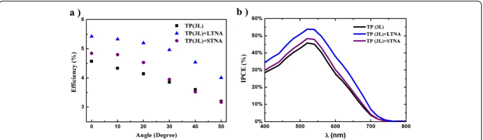
The I-V curves of the three types of DSSCs under lower irradiation (0.5 Sun) were also measured (Additional file 1: Figure S3). Owing to the excellent scattering property of the LTNA layer, an efficiency of 6.36% was achieved in the TP (3L) + LTNA cell, in comparison with the efficien-cies of 5.23% and 5.64% achieved in the TP (3L) and TP (3L) + STNA cells, respectively. The angular response of the three types of DSSCs was also investigated and com-pared (Figure 3a). Due to the high scattering power of the LTNA layer for the different photon propagation directions, the enhanced light absorption effect is less sensitive to the tilting of the cells.
The incident photon-to-current conversion efficiency (IPCE) spectra are depicted in Figure 3b to provide detailed information on light harvesting. It is observed that the main light harvesting enhancement caused by the scattering layer occurs not only in the dye absorption range but also in the long wavelength side [24,25], which is exactly the wave-length range for the small dye absorption. Consequently, the TP (3L) + LTNA cell is able to more efficiently recap-ture the unabsorbed light which resulted from the efficient light scattering capability of the LTNA layer. A further insight into the electrochemical behavior was provided by
the EIS measurement in the dark at different applied bias voltages. The electron recombination time (τn) was calculated from the Bode phase plots by τn= 1/ (2πfpeak), where fpeak is the characteristic peak fre-quency in the mid-frefre-quency (1 to 100 Hz) region [5,26]. As shown in Additional file 1: Figure S4, the use of the light scattering layer does not significantly
influ-ence the τn and hence does not affect the electron
transport.
Conclusions
Large-diameter TiO2 nanotube arrays were successfully synthesized. The outstanding scattering power of the LTNA layer was demonstrated by the transmittance spectra and the optical simulation. The LTNA layer is superior to the STNA one in terms of light scattering. The use of the LTNA as the scattering layer in DSSCs enhances the PCE (from 5.18% to 6.15%) and the short-circuit current density much more than the STNA does. It is believed that the large-diameter nanotubes can be applied to other types of solar cells and higher conver-sion efficiency can be achieved by further optimization.
Additional file
Additional file 1:Supporting information.Figure S1 The normalized and simulated transmittance spectra of the three types of photoanodes adhered to the FTO glass substrates before the sensitization with N719. Figure S2 (a) Photocurrent-voltage curves and (b) photovoltaic properties of the TP based DSSCs with different thickness. Figure S3 (a) Photocurrent-voltage curves under 0.5 Sun and (b) photovoltaic properties of the TP(3 L) based DSSCs coupled with different scattering layers, i.e., LTNA and STNA with the same thickness of 1.8μm. Figure S4 Electron lifetime of three types of DSSCs in the dark at different applied bias voltages.
Competing interests
[image:4.595.58.540.89.229.2]The authors declare that they have no competing interests.
Authors’contributions
XC and HH proposed the idea and presided over the study. XL, MG, JC, and YT conceived and designed the experiment. XL and JL wrote the paper. All authors read and approved the final manuscript.
Acknowledgements
The work was supported by grants received from the Research Grants Council of the Hong Kong Special Administrative Region (Project Nos. PolyU5159/13E and PolyU5163/12E) and the Hong Kong Polytechnic University (Project No. G-YL06). The work was also supported by the National Natural Science Foundation of China (Grant No. 61125503) and the Foundation for Development of Science and Technology of Shanghai (Grant No. 11XD1402600).
Received: 19 May 2014 Accepted: 9 July 2014 Published: 20 July 2014
References
1. O'Regan B, Grätzel M:A low-cost, high-efficiency solar cell based on dye-sensitized colloidal TiO2films.Nature1991,353:737.
2. Yella A, Lee H, Tsao H, Yi C, Chandiran A, Nazeeruddin M, Diau E, Yeh C, Zakeeruddin S, Grätzel M:Porphyrin-sensitized solar cells with cobalt (II/III)-based redox electrolyte exceed 12 percent efficiency.Science2011,
334:629–634.
3. Miao Q, Wu L, Cui J, Huang M, Ma T:A new type of dye-sensitized solar cell with a multilayered photoanode prepared by a film-transfer technique. Adv Mater2011,23:2764.
4. Kamat P:Quantum dot solar cells. Semiconductor nanocrystals as light harvesters.J Phys Chem C2008,112:18737.
5. Lin J, Liu X, Guo M, Lu W, Zhang G, Zhou L, Chen X, Huang H:A facile route to fabricate an anodic TiO2nanotube-nanoparticle hybrid
structure for high efficiency dye-sensitized solar cells.Nanoscale2012,
4:5148–5153.
6. Liu X, Lin J, Chen X:Synthesis of long TiO2nanotube arrays with a
small diameter for efficient dye-sensitized solar cells.RSC Adv2013,
3:4885–4889.
7. Lin J, Guo M, Yip G, Lu W, Zhang G, Liu X, Zhou L, Chen X, Huang H:
High temperature crystallization of free-standing anastase TiO2
nanotube membranes for high efficiency dye-sensitized solar cells. Adv Funct Mater2013,23:5952.
8. Lu H, Deng K, Shi Z, Liu Q, Zhu G, Fan H, Li L:Novel ZnO microflowers on nanorod arrays: local dissolution-driven growth and enhanced light harvesting in dye-sensitized solar cells.Nanoscale Res Lett2014,9:183. 9. Yoon J, Jang S, Vittal R, Lee J, Kim K:TiO2nanorods as additive to TiO2
film for improvement in the performance of dye-sensitized solar cells. J Photoch Photobio A2006,180:184–188.
10. Liu Z, Su X, Hou G, Bi S, Xiao Z, Jia H:Mixed photoelectrode based on spherical TiO2nanorod aggregates for dye-sensitized solar cells with
high short-circuit photocurrent density.RSC Adv2013,3:8474–8479. 11. Dadgostar S, Tagabadi F, Taghavinia N:Mesoporous submicrometer TiO2
hollow spheres as scatterers in dye-sensitized solar cells.ACS Appl Mater Interfaces2012,4:2964–2968.
12. Park Y, Chang Y, Kum B-G, Kong E, Son J, Kwon Y, Park T, Jang H:Size-tunable mesoporous spherical TiO2as a scattering overlayer in high-performance
dye-sensitized solar cells.J Mater Chem2011,21:9582.
13. Hwang S, Kim C, Song H, Son S, Jang J:Designed architecture of multiscale porous TiO2nanofibers for dye-sensitized solar cells
photoanode.ACS Appl Mater Interfaces2012,4:5287–5292. 14. Raza S, Toscano G, Jauho A, Mortensen N, Wubs M:Refractive-index
sensing with ultrathin plasmonic nanotubes.Plasmonics2012,8:193–199. 15. Chen Y, Chang Y, Huang J, Chen I, Kuo C:Light scattering and enhanced
photoactivities of electrospun titania nanofibers.J Phys Chem C2012,
116:3857–3865.
16. Lin J, Chen J, Chen X:Facile fabrication of free-standing TiO2nanotube
membranes with both ends open via self-detaching anodization. Electrochem Commun2010,12:1062–1065.
17. Valota A, LeClere D, Schmuki P, Curioni M, Hashimoto T, Berger S, Kunze J, Schmuki P, Thompson G:Influence of water content on nanotubular anodic titania formed in fluoride/glycerol electrolytes.Electrochim Acta
2009,54:4321–4327.
18. Sun L, Zhang S, Sun X, He X:Effect of the geometry of the anodized titania nanotube array on the performance of dye-sensitized solar cells. J Nanosci Nanotechnol2010,10:4551–4561.
19. Ni J, Noh K, Frandsen C, Kong S, He G, Tang T, Jin S:Preparation of near micrometer-sized TiO2nanotube arrays by high voltage anodization. Mater Sci Eng C2013,33:259–264.
20. So S, Lee K, Schmuki P:Ultrafast growth of highly ordered anodic TiO2
nanotubes in lactic acid electrolytes.J Am Chem Soc2012,134:11316–11318. 21. Guo M, Xie K, Lin J, Yong Z, Yip C, Zhou L, Wang Y, Huang H:Design and
coupling of multifunctional TiO2nanotube photonic crystal to
nanocrystalline titania layer as semi-transparent photoanode for dye-sensitized solar cell.Energy Environ Sci2012,5:9881–9888. 22. Yip CT, Huang H, Zhou L, Xie K, Wang Y, Feng T, Li J, Tam W:Direct and
seamless coupling of TiO2nanotube photonic crystal to dye-sensitized
solar cell: a single-step approach.Adv Mater2011,23:5624–5628. 23. Zhang Q, Myers D, Lan J, Jenekhe S, Cao G:Applications of light scattering
in dye-sensitized solar cells.Phys Chem Chem Phys2012,14:14982–14998. 24. Huang F, Chen D, Zhang X, Caruso R, Cheng Y:Dual-function scattering
layer of submicrometer-sized mesoporous TiO2beads for high-efficiency
dye-sensitized solar cells.Adv Funct Mater2010,20:1301–1305. 25. Chang Y, Kong E, Park Y, Jang H:Broadband light confinement using a
hierarchically structured TiO2multi-layer for dye-sensitized solar cells. J Mater Chem A2013,1:9707–9713.
26. Kern R, Sastrawan R, Ferber J, Stangl R, Luther J:Modeling and
interpretation of electrical impedance spectra of dye solar cells operated under open-circuit conditions.Electrochim Acta2002,47:4213.
doi:10.1186/1556-276X-9-362
Cite this article as:Liuet al.:Large-diameter titanium dioxide nanotube arrays as a scattering layer for high-efficiency dye-sensitized solar cell.
Nanoscale Research Letters20149:362.
Submit your manuscript to a
journal and benefi t from:
7Convenient online submission 7Rigorous peer review
7Immediate publication on acceptance 7Open access: articles freely available online 7High visibility within the fi eld
7Retaining the copyright to your article