N A N O E X P R E S S
Open Access
High Efficiency, Low Power-Consumption
DFB Quantum Cascade Lasers Without
Lateral Regrowth
Zhi-Wei Jia
1,2, Li-Jun Wang
1,2*, Jin-Chuan Zhang
1, Feng-Qi Liu
1,2*, Yu-Hong Zhou
1,2, Dong-Bo Wang
1,2,
Xue-Feng Jia
1,2, Ning Zhuo
1, Jun-Qi Liu
1,2, Shen-Qiang Zhai
1and Zhan-Guo Wang
1,2Abstract
Very low power-consumption distributed feedback (DFB) quantum cascade lasers (QCLs) at the wavelength around 4.9μm were fabricated by conventional process without lateral regrowth of InP:Fe or using sidewall grating. Benefitted from the optimized materials and low waveguide loss, very low threshold current density of 0.5 kA/cm2 was obtained for a device with cavity length of 2 mm. Combined with the partial-high-reflection coating, the 1-mm-long DFB QCL achieved low power-consumption continuous wave (CW) operation up to 105 °C. The CW threshold power-consumptions were 0.72 and 0.78 W at 15 and 25 °C, respectively. The maximum CW output power was over 110 mW at 15 °C and still more than 35 mW at 105 °C. At 15 °C, wall-plug efficiency of 5.5% and slope efficiency of 1.8 W/A were deduced, which were very high for low power-consumption DFB QCLs.
Keywords:Quantum cascade laser, Distributed feedback, Low power-consumption, High efficiency
Background
In recent years, quantum cascade lasers (QCLs) have proven to be very efficient coherent light sources in the mid-infrared region with a wide variety of applications, such as trace gas sensing, high-resolution spectroscopy, and free space communication [1–3]. Since the inven-tion of QCLs [4], distributed feedback (DFB) QCLs have also attracted much attention for their single longitu-dinal mode operation and compact module [5–7]. In portable applications, the input electrical power con-sumption of the DFB QCL is required to be as low as possible, so that the total volume and power consump-tion of the system can be minimized. Moreover, in order to obtain stable and narrow line-width single-mode emission, continuous wave (CW) operation of DFB QCL above ambient temperature is desired. Several works on the demonstration of room temperature, low power-consumption DFB QCLs have been reported, in which narrow ridge and short cavity device structure are the
common approach to lower the power consumption, with the typical ridge width of 2–5μm [8–10]. However, the narrow ridge width will increase the waveguide loss due to the lateral optical absorption and scattering, leading to a high threshold current density (Jth) and pre-venting the high temperature CW operation. To reduce waveguide loss of narrow ridge devices, the buried heterostructure (BH) configuration is necessary, which involves a complex fabrication process. Meanwhile, the BH structure reduces the optical confinement factor, which is also against to achieve low Jth operation. In [11], Briggs et al. used sidewall grating as an alternative to the BH structure, but the loss is still high for the narrow ridge width (4 μm). As the result, the Jth was high (1.91 kA/cm2 at 20 °C). In short, narrow ridge structure can lower the threshold current and power consumption at the expenses ofJth, slope efficiency, and wall-plug efficiency (WPE), which is not helpful to further reduce power consumption. The complex process and high cost are also unfavorable to the fabrica-tion and applicafabrica-tion of DFB QCLs.
In a previous report, we demonstrated the very low threshold operation of QCL in CW mode with theJthof 0.56 kA/cm2at 20 °C by optimizing growth parameter of * Correspondence:[email protected];[email protected]
1Key Laboratory of Semiconductor Materials Science, Institute of
Semiconductors, Chinese Academy of Sciences, Key Laboratory of Low Dimensional Semiconductor Materials and Devices, Beijing 100083, China Full list of author information is available at the end of the article
the epitaxial materials, wide ridge width was used to lower the waveguide loss and no lateral regrowth of InP:Fe was necessary [12]. The very low Jth is encour-aging for developing low power-consumption DFB QCLs without a very narrow ridge.
In this work, an active region based on two-phonon resonance design was modified and optimized. DFB QCLs with ridge width of 9 μm were fabricated by a conventional process without regrowth of InP:Fe or using sidewall grating. At 20 °C, the DFB QCLs with high-reflection (HR) coating and different cavity lengths (1, 1.5, and 2 mm) can all achieve CW single-mode operation with low Jth (0.84, 0.52, and 0.5 kA/cm2). In order to reduce the high mirror loss of short cavity devices, partial-high-reflection (PHR) coating consisting of Al2O3/Ge was designed and used [13]. After PHR coating on the front facet, the CWJthof the 1-mm-long device was reduced to 0.64 and 0.69 kA/cm2at 15 and 25 °C corresponding to the power consumptions of 0.72 and 0.78 W, respectively. Single-mode emission was main-tained from 15 to 105 °C, and the lasing wavenumber at 150 mA was tuned from 2045.5 to 2031.2 cm−1; no mode hopping was observed. The maximum CW output power was over 110 mW at 15 °C and still more than 35 mW at 105 °C. Wall-plug efficiency (WPE) of 5.5% and slope effi-ciency of 1.8 W/A were deduced at 15 °C, which were very high for low power-consumption DFB QCLs.
Methods
The QCL active region was based on the two-phonon resonant design, consisting of strain compensated In0.67Ga0.33As/In0.37Al0.63As superlattice, which was similar to that in ref. [14]. In order to obtain the lasing wavelength around 4.9 μm, the active region structure of ref. [14] was modified. The thicknesses of In0.67Ga0.33As quantum well layers were increased by 8%. According to our theoretical simulation on the modified active region structure, the dipole matrix element and the phonon scattering lifetime between
the upper laser level and the lower laser level were 1.60 nm and 2.55 ps, respectively. The simulation re-sults indicated that high performance can be main-tained compared to ref. [14]. Moreover, the drop of the transition levels in the modified structure lead to lower electric field intensity, meaning the decrease of operating voltage.
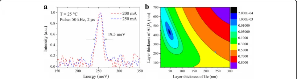
In order to minimize the free carrier absorption loss in the n-doped (S, 2 × 1017 cm−3) InP substrate and improve the material quality, a 3-μm-thick low-doped (Si, 2 × 1016 cm−3) InP layer was first grown on the substrate by metal organic vapor phase epitaxy (MOVPE). Then the 40-stage active region with the total thickness of 2.1 μm sandwiched between two 300-nm-thick lattice-matched InGaAs confinement layers were grown by solid-source molecular beam epitaxy (MBE) following the optimized growth control described in ref. [12]. The thicker active region can enhance the optical confinement factor and reduce Jth. High interface quality was achieved as indicated by the electrolumin-escence (EL) spectra given in Fig. 1a, which has a narrow full-width-at-half-maximum (FWHM) of 19.5 meV. This was important for low Jth operation, because sharp interface can reduce interface scattering for both electrons and photons. The buried DFB grating was patterned on the upper InGaAs layer, followed by the growth of upper InP layers by MOCVD. The design of the DFB grating was based on finite-element method by using the commercial software COMSOL. The grating was fabricated by holographic lithography and wet etching. The period and depth of the grating were 759 and 150 nm, respectively. The upper InP layers included a 3-μm-thick low-doped (Si, 2 × 1016 cm−3) InP layer, a 200-nm-thick gradual-doped (Si, 1–3 × 1018 cm−3) InP layer, and a 500-nm-thick high-doped (Si, 8 × 1018 cm−3) InP layer. With the gradual-doped layer, a sharp drop of carrier concentration could be avoided, which was beneficial to electric injection and removing surface plasma absorption. Then the wafer was processed into the
Fig. 1aElectroluminescence spectra of the wafer andbreflectivity of the Al2O3/Ge coating for the wavelength of 4.9μm as a function of the
[image:2.595.57.539.574.703.2]standard double-channel ridge waveguide lasers, which were simpler and low cost than the lasers with BH fabrication process. The processing details were similar to those in ref. [6]. The laser ridge width was 9μm, and the laser chips were cleaved into different cavity lengths of 1, 1.5, and 2 mm. After HR coating on the back facet, the lasers were bonded epi-layer side down on an AlN submount with AuSn solder, wire bonded, and then soldered on a copper heat sink.
To lower the mirror loss for short cavity DFB QCL, a partial-high-reflection (PHR) coating consisting of Al2O3/Ge was deposited on the front facet of the device by electron beam evaporation. The design of Al2O3/Ge coating was based on the concept of optical admittance [15]. The reflectivity (R) of the Al2O3/Ge coating for the wavelength of 4.9 μm as a function of the thicknesses of the two layers is plotted in Fig. 1b. As shown, the reflectivity of the Al2O3/Ge coating can be varied from 3.85 × 10⁻⁴ to more than 0.9 by changing the thicknesses of the two layers. Here we chose the thickness of Al2O3 and Ge to be 220 and 240 nm, corresponding to R~ 0.5, as marked by the blue star. It should be pointed out that since the wave-guide loss of a specific device cannot be obtained accurately and the coating layer thicknesses cannot be
controlled precisely by electron beam evaporation, the choice ofR~ 0.5 was not optimal, only with the purpose to lower theJth.
Results and Discussion
The lasers were mounted on a thermoelectrically cooled holder with a thermistor for monitoring and adjusting the heat sink temperature. The optical power and spec-tra from front facets of the lasers were measured with a calibrated thermopile detector placed directly in front of the laser facets and a Fourier transform infrared (FTIR) spectrometer, respectively.
Low Threshold Continuous Wave Operation
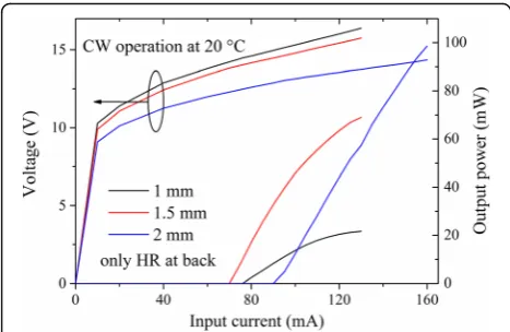
Figure 2 shows the CW power-current-voltage (PIV) characterization of three DFB QCLs with the cavity lengths of 1, 1.5, and 2 mm and ridge width of 9 μm. These data were measured at the heat sink temperature of 20 °C, from the devices with HR coating on the back facet and no coating on the front facet. The operating voltage decreased as the cavity length increased. The threshold currents (Ith) of 1-, 1.5-, and 2-mm-long devices were 76, 70, and 90 mA, respectively, with the corresponding Jth of 0.84, 0.52, and 0.5 kA/cm2. The maximum CW output power were 22, 69, and 99 mW for 1-, 1.5-, and 2-mm-long devices. It is noticed that the Jth of a 1-mm-long device was remarkably higher, which could be further improved by PHR coating.
[image:3.595.56.290.87.239.2]High Temperature Low Power-Consumption Performance After the CW measurement above, an Al2O3/Ge coating consisting of 220-nm-thick Al2O3and 240-nm-thick Ge was deposited on the front facet of the 1-mm-long DFB QCL. The 1-mm-long device with both HR and PHR coatings realized very high CW performance, includ-ing high temperature, low power-consumption, high output power, stable single-mode emission, and high slope efficiency.
Figure 3a shows the CW PIVcharacterization of the 1-mm-long device with both HR and PHR coatings over a heat sink temperature range from 15 to 105 °C. Fig. 2Typical CWPIVcharacterization of the DFB QCLs with different
cavity lengths of 1, 1.5, and 2 mm and ridge width of 9μm
[image:3.595.57.539.589.714.2]At 15 °C, the CW Ith and Jth were 57.4 mA and 0.64 kA/cm2, corresponding to the power consumption of 0.72 W. The maximum output power was more than 110 mW at the input electrical power-consumption of 2.2 W. As the heat sink temperature increased, the Ith increased to 115 mA and the maximum output power was still 36 mW at 105 °C. Limited by the heat sink temperature adjusting stage, we believe that the 1-mm-long device can operate well above 105 °C. The low-power consumption and high operating temperature mean that the cooling system for removing the heat can be simplified or even removed, which is significant to many applications. In addition, high temperature and low power-consumption performance was also import-ant for applications in harsh thermal environments. The Jth and maximum slope efficiency (ηs) were also plotted as the functions of the heat sink temperature in Fig. 3b. Theηswas 1.8 W/A at 15 °C and about 1.0 W/A at 105 °C, which is much higher than the previously reportedηsvalues [8–11]. The characteristic temperatures
T0 and T1 for threshold current density and slope effi-ciency were 129 and 156 K, respectively. Both the lowJth and high ηs were excellent values for short cavity low power-consumption DFB QCLs, meaning high WPE in CW mode for the 1-mm-long device.
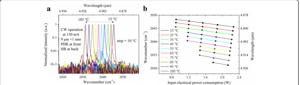
Figure 4a shows the CW lasing spectra of the 1-mm-long PHR and HR-coated DFB QCL at 150 mA with the heat sink temperatures ranging from 15 to 105 °C. As shown, the single mode emission with the side-mode-suppression ratio (SMSR) above 20 dB was tuned from 2045.5 to 2031.2 cm−1 as the temperature increased from 15 to 105 °C. The CW lasing wavenumber was also plotted as a function of input electrical power-consumption and heat sink temperature in Fig. 4b. It can be observed that the lasing wavenumber was tuned linearly with the input electrical power-consumption and heat sink temperature over the whole measured range, which indicates that stable single mode oper-ation was maintained without mode hopping behavior.
As shown, the performance of the 1-mm-long DFB QCL was improved significantly by the PHR coating. We expect to further reduce the power consumption of our DFB QCL by shortening the cavity length and using higher reflectivity PHR coating.
High Wall-Plug Efficiency
From Fig. 3a, the CW WPE was calculated and plotted as a function of the input electrical power-consumption in Fig. 5. At 15 °C, a maximum WPE of 5.5% was obtained around 125 mA with the output power of 100 mW. The maximum WPE were still 3.5 and 1.5% at 55 and 105 °C. To date, these values were very high for the DFB QCLs with the threshold power-consumption less than 1 W. It is believed that the WPE can be further improved by the precise facets coating technology and the optimized active region structure such as shallow-well design.
Fig. 4aCW lasing spectra of the 1-mm-long PHR and HR-coated DFB QCL at 150 mA with different heat sink temperatures andbCW lasing wavenumber as a function of input electrical power-consumption and heat sink temperature
[image:4.595.57.541.89.226.2] [image:4.595.306.539.528.702.2]Conclusions
Very low power-consumption DFB QCLs were fabri-cated by conventional process without lateral regrowth or using sidewall grating. The lowJthroom temperature CW operation was demonstrated, which can be attribu-ted to the optimized materials and low waveguide loss. The 1-mm-long PHR and HR-coated DFB QCL achieved very high CW performance, including high operating temperature (up to 105 °C), low threshold power-consumption (0.72 and 0.78 W at 15 and 25 °C), stable single-mode emission (SMSR >20 dB and mode-hopping free), high WPE of 5.5% and high slope effi-ciency of 1.8 W/A at 15 °C. The maximum CW output power was over 110 mW at 15 °C and still more than 35 mW at 105 °C. Compared with the previous reports on low power-consumption DFB QCLs, the fabrication process was simple and low cost. Meanwhile, the high temperature CW operation with low power-consumption allowed for more compact laser package, which is signifi-cant to develop portable laser system and for applications in harsh thermal environments.
Abbreviations
BH:Buried heterostructure; CW: Continuous wave; DFB: Distributed feedback; EL: Electroluminescence; FTIR: Fourier transform infrared; FWHM: Full-width-at-half-maximum; HR: High reflection;Ith: Threshold current;Jth: Threshold
current density; MBE: Molecular beam epitaxy; MOVPE: Metal organic vapor phase epitaxy; PHR: Partial-high-reflection;PIV: Power-current-voltage; QCL: Quantum cascade laser;R: Reflectivity; SMSR: Side-mode-suppression ratio; WPE: Wall-plug efficiency;ηs: Slope efficiency
Acknowledgements
The authors acknowledge the contributions of Ping Liang and Ying Hu in the device fabrication.
Funding
This work was supported by the National Basic Research Program of China (Grant Nos. 2013CB632803/01), National Key Research and Development Program (Grant No. 2016YFB0402303), National Natural Science Foundation of China (Grant Nos. 61435014, 61627822, 61574136, 61404131), Key Projects of Chinese Academy of Sciences (Grant No. ZDRW-XH-2016-4), and Beijing Natural Science Foundation (Grant No. 4162060, 4172060).
Authors’Contributions
ZWJ designed the device structure, fabricated the device, performed the testing, and wrote the paper. LJW and FQL provided the concept, polished the paper, and supervised the project. JCZ and JQL improved the design. YHZ and SQZ performed the testing. DBW and XFJ completed the MOCVD growth. NZ modulated the active region structure and completed the MBE growth. ZGW supervised the project. All authors read and approved the final manuscript.
Competing Interests
The authors declare that they have no competing interests.
Publisher’s Note
Springer Nature remains neutral with regard to jurisdictional claims in published maps and institutional affiliations.
Author details
1Key Laboratory of Semiconductor Materials Science, Institute of
Semiconductors, Chinese Academy of Sciences, Key Laboratory of Low Dimensional Semiconductor Materials and Devices, Beijing 100083, China.
2College of Materials Science and Opto-Electronic Technology, University of
Chinese Academy of Sciences, Beijing 101408, China.
Received: 16 March 2017 Accepted: 7 April 2017
References
1. Dong L, Kosterev AA, Thomazy D, Tittel FK (2010) QEPAS spectrophones: design, optimization, and performance. Appl Phys B-Lasers Opt 100:627–635 2. Li J, Chen W, Fischer H (2013) Quantum cascade laser spectrometry techniques:
a new trend in atmospheric chemistry. Appl Spectrosc Rev 48:523–559 3. Liu C, Zhai S, Zhang J, Zhou Y, Jia Z, Liu F, Wang Z (2015) Free-space
communication based on quantum cascade laser. J Semicond 36:094009 4. Faist J, Capasso F, Sivco DL, Sirtori C, Hutchinson AL, Cho AY (1994)
Quantum cascade laser. Science 264:553–556
5. Faist J, Gmachl C, Capasso F, Sirtori C, Sivco DL, Baillargeon JN, Cho AY (1997) Distributed feedback quantum cascade lasers. Appl Phys Lett 70:2670–2672
6. Zhang J, Liu F, Tan S, Yao D, Wang L, Li L, Liu J, Wang Z (2012) High-performance uncooled distributed-feedback quantum cascade laser without lateral regrowth. Appl Phys Lett 100:112105
7. Yao D-Y, Zhang J-C, Cathabard O, Zhai S-Q, Liu Y-H, Jia Z-W, Liu F-Q, Wang Z-G (2015) 10-W pulsed operation of substrate emitting photonic-crystal quantum cascade laser with very small divergence. Nanoscale Res Lett 10:177 8. Hinkov B, Bismuto A, Bonetti Y, Beck M, Blaser S, Faist J (2012) Singlemode
quantum cascade lasers with power dissipation below 1 W. Electron Lett 48:646–647
9. Bismuto A, Blaser S, Terazzi R, Gresch T, Muller A (2015) High performance, low dissipation quantum cascade lasers across the mid-IR range. Opt Express 23:5477–5484
10. Wolf JM, Riedi S, Süess MJ, Beck M, Faist J (2016) 3.36μm single-mode quantum cascade laser with a dissipation below 250 mW. Opt Express 24:662–671
11. Briggs RM, Frez C, Borgentun CE, Forouhar S (2014) Regrowth-free single-mode quantum cascade lasers with power consumption below 1 W. Appl Phys Lett 105:141117
12. Yan F-L, Zhang J-C, Yao D-Y, Liu F-Q, Wang L-J, Liu J-Q, Wang Z-G (2015) Very low threshold operation of quantum cascade lasers. Chin Phys B 24:024212
13. Bai Y, Darvish S, Bandyopadhyay N, Slivken S, Razeghi M (2011) Optimizing facet coating of quantum cascade lasers for low power consumption. J Appl Phys 109:053103
14. Bai Y, Slivken S, Darvish S, Razeghi M (2008) Room temperature continuous wave operation of quantum cascade lasers with 12.5% wall plug efficiency. Appl Phys Lett 93:021103
15. Lee J, Tanaka T, Sasaki S, Uchiyama S, Tsuchiya M, Kamiya T (1998) Novel design procedure of broad-band multilayer antireflection coatings for optical and optoelectronic devices. J Lightwave Technol 16:884
Submit your manuscript to a
journal and benefi t from:
7 Convenient online submission
7Rigorous peer review
7 Immediate publication on acceptance
7Open access: articles freely available online
7 High visibility within the fi eld
7Retaining the copyright to your article