A Monthly Double-Blind Peer Reviewed Refereed Open Access International e-Journal - Included in the International Serial Directories. GE-International Journal of Engineering Research (GE-IJER)ISSN (O):(2321-1717), ISSN(P):(2394-420X)
59 | P a g e
NUMERICAL MODELING OF EMPIRICAL
PSEUDOPOTENTIAL METHOD FOR DEVICE SIMULATION
Adam Strickland and Prof. Hamid Fardi
Dept. of Electrical Engineering,
University of Colorado Denver| Anschutz Medical Campus, USA.
ABSTRACT
The topic of this article is to develop a computer program for finding band structures that can
be used in simulating semiconductor devices. Many current simulation tools use effective mass
approximations to model the propagation of electrons through a device. Because modern
devices take advantage of different materials, geometries and size, a band structure calculation
becomes necessary for representing effects such as strained materials and hot carriers,
electron velocity and mobility. It is desirable to calculate band structure within a device
simulation program such as composition dependent hetero-structures with different
composition gradients, strained lattices, or studying the effects of surface roughness in a
device. While highly accurate, calculation-intense methods exist, a band structure may need to
be recalculated on the fly creating the need for fast, simple algorithm that can be tailored for
the situation at hand. In this paper, empirical pseudopotential method is applied to simulate
band structures of CdTe, ZeTe, ZnSe, and ZnS important in the study of photovoltaic devices
and composition dependent SiGe as a hetero-structure material.
Keywords: Pseudopotential, Device Modeling, Hamiltonian, Heterojunctions.
Introduction:
The band structure of a material is important for studying optical and electronic properties. As
new materials are developed, there is a greater need for energy band calculations. Band
structure calculations can be used to engineer custom band structures to tailor optical or
GE-International Journal of Engineering Research
Vol. 4, Issue 9, September 2016 IF- 4.721 ISSN(O):(2321-1717), ISSN(P):(2394-420X)
© Associated Asia Research Foundation (AARF) Publication
A Monthly Double-Blind Peer Reviewed Refereed Open Access International e-Journal - Included in the International Serial Directories. GE-International Journal of Engineering Research (GE-IJER)ISSN (O):(2321-1717), ISSN(P):(2394-420X)
60 | P a g e
electrical devices. For calculating band structure there are two basic approaches: ab initio and
empirical methods. Ab initio, or “from the beginning” methods, involve calculation of band
structure by use of first- principles without using measured data. Empirical methods take
advantage of experimental data to give more accurate band structure representation. Generally,
ab initio methods are calculation intensive, but give better insight on how the structure arrives.
Both methods have their place in calculating and engineering transport properties in
semiconductor devices.
Because modern devices take advantage of different materials, a band structure calculation
becomes necessary for representing effects such as strained materials and hot carriers, electron
velocity and mobility [1, 2]. Band structure simulation within a device program for studying
the effects of surface roughness in a device is reported in [3, 4, 5]. While highly accurate,
calculation-intense methods exist, a band structure may need to be recalculated on the fly
creating the need for fast, simple algorithm that can be tailored for the situation at hand [6-10].
Examples of ab initio methods are the Hartree-Fock [11, 12] and Density Functional Theory
(DFT) [13]. Hartree-Fock method is based on Linear Combination of Atomic Orbitals
(LCAO) and uses the muffin-tin atom orbital as the method. Several other methods based on
LCAO can be employed. The DFT method projects the system of interacting particles into a
system of non- interacting particles. QuantumWise [14] is an example of a program that uses
ab initio methods for simulations. It will be shown that empirical method (EPM) can also be
used for materials without being as bulky as first principle based methods. Other methods such
as genetic algorithms have become highly utilized in many aspects of semiconductor devices.
The have been used find device parameters [15], band structure engineering [16], direct band
gap discovery [6], reconstruction of Scanning Tunneling Microscope (STM) imagery [17] and
even optimization of manufacturing devices. [18]. Recently genetic algorithms applied to EPM
has been used to calculate the band structure for 4H-SiC [19]. A detailed overview of genetic
A Monthly Double-Blind Peer Reviewed Refereed Open Access International e-Journal - Included in the International Serial Directories. GE-International Journal of Engineering Research (GE-IJER)ISSN (O):(2321-1717), ISSN(P):(2394-420X)
61 | P a g e
Modeling Pseudopotential band structure calculation:
Since core electrons in the inner shells of atoms are strongly bound, they do not play a significant
part in the electronic and optical properties. The Philips Kleinman cancellation theorem [21,
22] creates a smooth wave function to represent the core energies and potentials by taking
advantage of crystal symmetry, and allows for simple calculation of wave energies. The
previous method proposed by Herring in 1940 (and still of importance when core electrons
must be taken into ac- count) involved orthogonalizing each plane wave creating a linear
combination of core orbitals [23]. This method was successful in improving accuracy for
specific applications, but was admittedly laborious. Spherical symmetry of the core was lost
due to orthoganalizing a single plane wave to the core functions, and this limited its use to
metallic structures. In 1953 Slater effectively solved the symmetry issue by using Bloch waves
to represent the periodicity of a crystal. The final step was to smooth the contribution of the
core atoms by using an effective potential. The secondary benefit of doing this is that molecules
can also be modeled in the system and discusses the possibility of modifying the repulsive
potential to reproduce the free-atom term values [24]. EPM is a powerful method for calculating
band structure and studying the effects of changing boundaries during a simulation because it is
not as time-intensive as modern techniques must be developed to calculate band structures in
these scenarios. There are several modern approaches to find form factors for different
applications. First-principles calculations such as LCAO can be used to find pseudopotentials
A Monthly Double-Blind Peer Reviewed Refereed Open Access International e-Journal - Included in the International Serial Directories. GE-International Journal of Engineering Research (GE-IJER)ISSN (O):(2321-1717), ISSN(P):(2394-420X)
62 | P a g e
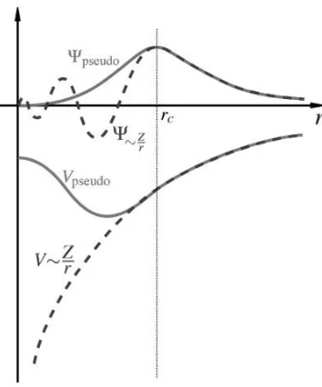
Figure 1. A graphical representation of pseudopotential simplification
Empirical Pseudopotential Method:
Orthogonal plane wave is the starting point for EPM. Figure 1. Shows a pseudopotential
simplification used in the model. By assuming s or p orbital atomic symmetry Ψk is constructed
to be orthogonal to the core states,
𝛹𝑘 = 𝜑𝑘 + 𝑎𝑡 𝑘,𝑡𝜙𝑘,𝑡 (1)
where ak,t are the orthogalization coefficients and φk,t are the core wave functions. We seek
a solution that gives ϕk as a smooth function. Using the Schrodinger equation,
H Ψk = E Ψk (2)
and substituting (2.1) into (2.2) we get,
𝐻𝜑𝑘+ 𝑎𝑡 𝑘,𝑡(𝐸 − 𝐸𝑡)𝜙𝑘,𝑡 = 𝐸𝜑𝑘 . (3)
Introducing
Vr = 𝑎𝑡 𝑘,𝑡(𝐸 − 𝐸𝑡)𝜙𝑘,𝑡/𝜑𝑘 (4)
where Vr represents the short-range repulsive potential; we have the desired form to find
[image:4.612.214.391.71.284.2]A Monthly Double-Blind Peer Reviewed Refereed Open Access International e-Journal - Included in the International Serial Directories. GE-International Journal of Engineering Research (GE-IJER)ISSN (O):(2321-1717), ISSN(P):(2394-420X)
63 | P a g e
(H +Vr) 𝜑𝑘=𝐸𝜑𝑘 (5)
By adding the Hamiltonian operator,
H = 𝑝
2
2𝑚 + Vc (6)
where Vc represents the core potential. Inserting (6) into (5), we get the eigenvalue problem,
(𝑝
2
2𝑚 + Vc + Vr) 𝜑𝑘 = 𝐸𝜑𝑘 (7)
It can be seen from (7) that the core and the short-range potentials can be added together to equal a
pseudopotential Vp = Vc + Vr , which is known as the Phillips-Kleinman cancellation
theorem. The eigenvalue energy of (7) is the actual energy of the crystal wave Φk . ϕk can be
thought of as the pseudo wave function. The actual contributions of each orbital can be added
up through LCAO to create Vp, but historically EPM used potentials measured empirically.
Model for Band Structure Simulation:
Solving the Schrodinger equation is all that is needed to find the band structure of a particular
material. Unfortunately, this is a nontrivial exercise. We will focus on discreet points along
the Brillouin Zone (BZ). Starting with the time independent Schrodinger equation,
[- ħ
2 2𝑚∇
2+ V(r)]Ψ
𝑘,𝑟 = 𝐸 𝑘 (8)
Both the wave function and the potential must be discretized. Since the wave function is periodic, it can be written in Bloch form and as a series,
Ψ 𝑘,𝑟 = 𝑒𝑖𝑘𝑟𝑢
𝑘 𝑟 = 𝑒𝑖𝑘𝑟 𝐴ℎ ℎ𝑒𝑖𝐾ℎ𝑟 (9)
where k is the crystal wave vector, r is the position and uk(r) is a periodic function with the same periodicity as the crystal. Similarly, the potential is periodic,
V(r) = 𝑉𝑚 𝑚𝑒𝑖𝐾𝑚𝑟 (10)
By substituting (9) and (10) into (8) we arrive at a nearly discrete function,
ħ2
2𝑚 𝑘 + 𝐾ℎ 2 𝐴
ℎ𝑒𝑖 𝑘+𝐾ℎ 𝑟
A Monthly Double-Blind Peer Reviewed Refereed Open Access International e-Journal - Included in the International Serial Directories. GE-International Journal of Engineering Research (GE-IJER)ISSN (O):(2321-1717), ISSN(P):(2394-420X)
64 | P a g e
To take advantage of orthogonality (11) is multiplied by ei(k+Kh)r and integrated to give,
ħ2
2𝑚 𝑘 + 𝐾ℎ 2 𝐴
ℎ𝛿ℎ,𝑙
ℎ + 𝑉𝑚 ℎ 𝑚𝐴ℎ𝛿𝑚 ,𝑙−ℎ = 𝐸(𝑘) 𝐴ℎ ℎ𝛿ℎ,𝑙 (12)
where δh,l are Kronecker delta functions. In other words,
𝛿ℎ,𝑙 = 1, ℎ = 𝑙
0, ℎ ≠ 𝑙 (13)
This can be simplified further since h = l only happens once for the first term of the left- hand side, h times for the second term and once for the right-hand side,
ħ2
2𝑚 𝑘 + 𝐾ℎ
2𝐴
ℎ + 𝑉ℎ 𝑚𝐴ℎ = 𝐸(𝑘)𝐴ℎ (14)
Equation (2.14) is an eigenvalue problem. All that is needed to find E(k) is to construct the
Hamiltonian and solve for the eigen values Hi,j :
𝐻𝑖,𝑗 =
ħ2
2𝑚 𝑘 + 𝐾ℎ
2𝛿
𝑖,𝑗 + 𝑉 (15)
Where
V=𝑉𝑆cos(𝐾𝑚. 𝜏) + 𝑖𝑉𝐴sin 𝐾𝑚. 𝜏 . (16)
Equation (16) accounts for two atoms per lattice point where the maximum offset is given by τ :
𝜏 = 𝑎(1
8, 1 8,
1
8) (17)
and VS are form factors measured experimentally eigen library calculating energies. We used
our program to simulate and calculate bands structure using form factors published in reference
[24]. Figures 2 through 5 show the results of program reduces to about 1 second per lattice
point. For both cases 98% of these times were spent in the seconds per lattice point. For
A Monthly Double-Blind Peer Reviewed Refereed Open Access International e-Journal - Included in the International Serial Directories. GE-International Journal of Engineering Research (GE-IJER)ISSN (O):(2321-1717), ISSN(P):(2394-420X)
65 | P a g e
Table 1: Form factors of ZnS, ZnSe, ZnTe, CdTe at 300K from [24].
a(˚A) V3S V8S V11S V3A V4A V11A
Si 5.43 -0.21 0.04 0.08 0 0 0
Ge 5.56 -0.23 0.01 0.06 0 0 0
Sn 6.49 -0.20 0 0.04 0 0 0
GaP 5.44 -0.22 0.03 0.07 0.12 0.07 0.02
GaAs 5.64 -0.23 0.01 0.06 0.07 0.05 0.01
AlSb 6.13 -0.21 0.02 0.06 0.06 0.04 0.02
InP 5.86 -0.23 0.01 0.06 0.07 0.05 0.01
GaSb 6.12 -0.22 0.00 0.05 0.06 0.05 0.01
InAs 6.04 -0.22 0.00 0.05 0.08 0.05 0.03
IsSb 6.04 -0.20 0.00 0.04 0.06 0.05 0.01
ZnS 5.41 -0.22 0.03 0.07 0.24 0.14 0.04
ZnSe 5.65 -0.23 0.01 0.06 0.18 0.12 0.03
ZnTe 6.07 -0.22 0.00 0.05 0.13 0.10 0.01
CdTe 6.41 -0.20 0.00 0.04 0.15 0.09 0.04
The actual code starts by creating two tables used during the actual calculation
process. The first table contains all of the k values. The second table is the pre-calculated
bottom half of the Hamiltonian matrix. The eigen solver library only needs the lower half if
the matrix is Hermitian. Since these values do not change for different k, they can be
pre-calculated [25]. Creating these tables reduces the execution time and simplifies the creation of
the Hamiltonian matrix in the main execution loop. Once these tables are created, the main
execution loop is started. The diagonals for a given k are calculated and added to the template
H matrix. After the Hamiltonian is built, the eigen library finds the eigenvalues for a given k.
It should be noted the number of points used for k determines the resolution for the Brillouin
Zone, while the number of K points determines the accuracy for these energies of eigen
values.
Results and Discussions:
The average run time for the simulation program is about 1 minute and 10
seconds. This includes calculating the eigen energies for 70, 124 × 124 Hamiltonian matrices
or about 10 seconds per lattice point. For materials such as Si or Ge where VA values are 0
[image:7.612.184.458.88.299.2]A Monthly Double-Blind Peer Reviewed Refereed Open Access International e-Journal - Included in the International Serial Directories. GE-International Journal of Engineering Research (GE-IJER)ISSN (O):(2321-1717), ISSN(P):(2394-420X)
66 | P a g e
re
la
ti
v
e
e
n
e
rg
y
[
e
V
]
were spent in the eigen library calculating energies. We used our program to simulate and
calculate bands structure using form factors published in reference [24]. Figures 2 through 5
show the results of program.
Table 2. Form factors of SiGe Alloy for different compositions at 300K
x a(˚A) V3S V8S V11S V3A V4A V11A
0.00 5.4300 -0.210 0.0400 0.080 0 0 0
0.25 5.4625 -0.215 0.0325 0.075 0 0 0
0.50 5.4950 -0.220 0.0250 0.070 0 0 0
0.75 5.5275 -0.225 0.0175 0.065 0 0 0
1.00 5.5600 -0.230 0.0100 0.060 0 0 0
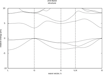
Figure 2. ZnS band structure with form factors from [24]
ZnS Band structure
10
5
0
-5
-10
L G X U,K G
[image:8.612.127.486.344.606.2]A Monthly Double-Blind Peer Reviewed Refereed Open Access International e-Journal - Included in the International Serial Directories. GE-International Journal of Engineering Research (GE-IJER)ISSN (O):(2321-1717), ISSN(P):(2394-420X)
67 | P a g e
re
la
ti
v
e
e
n
e
rg
y
[
e
V
[image:9.612.127.484.112.349.2]]
Figure 3. ZnSe band structure with form factors from [24]
ZnSe Band structure
10
5
0
-5
-10
L G X U,K G
A Monthly Double-Blind Peer Reviewed Refereed Open Access International e-Journal - Included in the International Serial Directories. GE-International Journal of Engineering Research (GE-IJER)ISSN (O):(2321-1717), ISSN(P):(2394-420X)
68 | P a g e
re
la
ti
v
e
e
n
e
rg
y
[
e
V
]
re
la
ti
v
e
e
n
e
rg
y
[
e
V
[image:10.612.127.484.137.371.2]]
Figure 4. InP band structure with form factors from [24]
InP Band structure
10
5
0
-5
-10
L G X U,K G
wave vector, k
Figure 5. CdTe band structure with form factors from [24]
CdTe Band structure
10
5
0
-5
-10
L G X U,K G
[image:10.612.106.555.434.712.2]A Monthly Double-Blind Peer Reviewed Refereed Open Access International e-Journal - Included in the International Serial Directories. GE-International Journal of Engineering Research (GE-IJER)ISSN (O):(2321-1717), ISSN(P):(2394-420X)
69 | P a g e
There are situations where it becomes desirable to do band calculations inside device
simulations where the band structure can change as a result of the operation of the device.
This is a good application for modeling using first principles to discover pseudopotentials
that could work for using EPM in the actual device. Ab initio approaches give insight into
engineering effective geometries, but they are limited to structures in the range of thousands
of atoms [26]. For any kind of large scale integration these methods fall short. EPM offers a
solution for devices with much larger number of atoms (2 x10⁵ atoms). Pseudopotentials
methods have become increasingly popular. Indeed, this in no longer empirical, but shows
the versatility of EPM for modeling modern materials [27]. Once band structure is known it
can be mapped into effective mass and/or mobility to lessen the computational burden in
actual device simulation. An example of this situation is demonstrated in reference [28].
Alloy Materials:
First principles techniques are able to make calculations based on specific atom locations.
This is of great use in studying boundary deformations. For some alloy materials there
is a known concentration, and there may be a known strain. For example, SiGe with
highly controlled composition can be epitaxially grown through the use of ultrahigh-vacuum
chemical vapor deposition [29]. Since these materials are quasi homogeneous virtual crystal
approximation allows the properties of two atoms to be used to make a hybrid atom [5]. For
this method the strained lattice and the form factors are function of the composition
percentage. The strained lattice can be represented as:
at(x) = a1(1 − x) + a2x (18)
Similarly, the form factors can be calculated as:
V t(x) = V1(1 − x) + V2 (19)
Table 2 shows the parameters of SiGe alloy at differing compositions, and figure 3.1
shows progression of how the band structure changes. The method for calculating the band
structure is the same as above. It can be seen that the top band in figure 3.2(a) starts to pull
down in 3.2(b), and by 3.2(c) at a concentration of x = 50% that same band is below the normal
conduction band of Silicon. At x = 75% the alloy becomes Germanium-like as the direct band
A Monthly Double-Blind Peer Reviewed Refereed Open Access International e-Journal - Included in the International Serial Directories. GE-International Journal of Engineering Research (GE-IJER)ISSN (O):(2321-1717), ISSN(P):(2394-420X)
70 | P a g e
re la ti ve e n e rg y [ e V ] re la ti ve e n e rg y [ e V ] re la ti ve e n e rg y [ e V ] re la ti ve e n e rg y [ e V ] re la ti ve e n e rg y [ e V ]
Figure 6: The Band Structure for Different Concentrations of Silicon-Germanium Alloy
Si Bandstructure SiGe25 Bandstructure
10 10
5 5
0 0
-5 -5
-10
L G X U,K G
wave vector, k
(a) x = 0%
-10
L G X U,K
G wave vector, k
(b) x = 25%
SiGe50 Bandstructure SiGe75 Bandstructure
10 10
5 5
0 0
-5 -5
-10
L G X U,K G
wave vector, k
(c) x = 50%
-10
L G X U,K
G wave vector, k
(d) x = 75%
Ge Bandstructure 10 5 0 -5 -10
L G X U,K G
wave vector, k
A Monthly Double-Blind Peer Reviewed Refereed Open Access International e-Journal - Included in the International Serial Directories. GE-International Journal of Engineering Research (GE-IJER)ISSN (O):(2321-1717), ISSN(P):(2394-420X)
71 | P a g e
References:
1. Enzo Ungersboeck, Siddhartha Dhar, Gerhard Karlowatz, Viktor Sverdlov, Hans Kosina,
and Siegfried Selberherr. The Effect of General Strain on the Band Structure and
Electron Mobility of Silicon, volume 54. IEEE Transactions on Electron Devices, Sep
2007.
2. Y.W. Wen, H.J. Liu, L. Pan, X.J. Tan, H.Y. Lv, J. Shi, and X.F. Tang. Reducing the
thermal conductivity of silicon by nanostructure patterning. Applied Physics A,
110(1):93–98, 2013.
3. Richard A. Coles. Theory of the Electronic States of Semiconductor Heterostructures.
PhD thesis, Durham University, March 1999.
4. Massimo V. Fischetti and Sudarshan Narayanan. An empirical pseudopotential approach
to surface and line-edge roughness scattering in nanostructures: Application to si thin
films and nanowires and to graphene nanoribbons. Journal of Applied Physics, 110(8):–,
2011.
5. Salvador Gonzalez, Dragica Vasileska, and AlexanderA. Demkov. Empirical
pseudopotential method for the band structure calculation of strained-silicon germanium
materials. Journal of Computational Electronics, 1(1-2):179–183, 2002.
6. Mayeul d’Avezac, Jun-Wei Luo, Thomas Chanier, and Alex Zunger.
Genetic-algorithm dis- covery of a direct-gap and optically allowed superstructure from
indirect-gap si and ge semi- conductors. Phys. Rev. Lett., 108:027401, Jan 2012.
7. A. De and Craig E. Pryor. Predicted band structures of iii-v semiconductors in the
wurtzite phase. Phys. Rev. B, 81:155210, Apr 2010.
8. Stephen M. Goodnick Dragica Vasileska, editor. Nano-Electronic Devices: Semiclassical
and Quantum Transport Modeling. Springer Science+Business Media, 2011.
9. N. D. Drummond, V. Z´olyomi, and V. I. Fal’ko. Electrically tunable band gap in
A Monthly Double-Blind Peer Reviewed Refereed Open Access International e-Journal - Included in the International Serial Directories. GE-International Journal of Engineering Research (GE-IJER)ISSN (O):(2321-1717), ISSN(P):(2394-420X)
72 | P a g e
10. Aniello Esposito. Band Structure Effects and Quantum Transport. PhD thesis, ETH
ZURICH, 2010.
11. A. Svane. Hartree-fock band-structure calculations with the linear muffin-tin-orbital
method: Application to c, si, ge. Phys. Rev. B, 35:5496–5502, Apr 1987.
12. P. Bowlan, E Martinez-Moreno, K Reimann, M Woerner, and T Elsaesser.
Terahertz radiative coupling and damping in multilayer graphene. New Journal of
Physics, 16(1):013027, 2014.
13. I. N. Remediakis and Efthimios Kaxiras. Band-structure calculations for semiconductor
within generalized-density-functional theory. Phys. Rev. B, 59:5536–5543, Feb 1999.
14. Quantumwise atomistix toolkit (atk).
15. Fang Feng-bo and Wu Tao. Genetic algorithm and semiconductor device model
parameter extraction. In Genetic and Evolutionary Computing, 2009. WGEC ’09. 3rd
International Conference on, pages 97–100, Oct 2009.
16. Kwiseon Kim, Peter A. Graf, and Wesley B. Jones. A genetic algorithm based inverse
band structure method for semiconductor alloys. Journal of Computational Physics,
208(2):735 – 760, 2005.
17. F.C. Chuang, C.V. Ciobanu, V.B. Shenoy, C.Z. Wang, and K.M. Ho. Finding the
reconstruc- tions of semiconductor surfaces via a genetic algorithm. Surface Science,
573(2):L375 – L381, 2004.
18. Shuo Wang and Reha Uzsoy. A genetic algorithm to minimize maximum lateness on a
batch processing machine. Computers and Operations Research, 29(12):1621 – 1640,
2002.
19. G. Ng, D. Vasileska, and D.K. Schroder. Empirical pseudopotential band structure
parameters of 4h-sic using a genetic algorithm fitting routine. Superlattices and
A Monthly Double-Blind Peer Reviewed Refereed Open Access International e-Journal - Included in the International Serial Directories. GE-International Journal of Engineering Research (GE-IJER)ISSN (O):(2321-1717), ISSN(P):(2394-420X)
73 | P a g e
20.E.A.B. Cole. Overview of device modelling. In Mathematical and Numerical
Modelling of Heterostructure Semiconductor Devices: From Theory to Programming,
pages 3–20. Springer London, 2009.
21.Jiseok Kim and Massimo V. Fischetti. Empirical pseudopotential calculations of the band
structure and ballistic conductance of strained [001], [110], and [111] silicon nanowires.
Journal of Applied Physics, 110(3): 2011.
22.James C. Phillips and Leonard Kleinman. New method for calculating wave
functions in crystals and molecules. Phys. Rev., 116:287–294, Oct 1959.
23.Conyers Herring. A new method for calculating wave functions in crystals. Phys. Rev.,
57:1169– 1177, Jun 1940.
24.Marvin L. Cohen and T. K. Bergstresser. Band structures and pseudopotential form
factors for fourteen semiconductors of the diamond and zinc-blende structures. Phys.
Rev., 141:789–796, Jan 1966.
25.
et al Gel Guennebaud, Benoit Jacob. Eigen v3, 2010.
26.
Massimo V Fischetti, Jiseok Kim, Sudarshan Narayanan, Zhun-Yong Ong,
Catherine Sachs, David K Ferry, and Shela J Aboud. Pseudopotential-based studies
of electron transport in graphene and graphene nanoribbons. Journal of Physics:
Condensed Matter, 25(47):473202, 2013.
27. M. V. Fischettia and S. E. Laux. Band structure, deformation potentials, and carrier
mobility in strained Si, Ge, and SiGe alloys, volume 80. J. Appl. Phys., 1996.
28. Bernard S. Meyerson, Kevin J. Uram, and Francoise K. LeGoues. Cooperative
growth phenom- ena in silicon/germanium lowtemperature epitaxy. Applied Physics
Letters, 53(25):2555–2557, 1988.
29. Jeff Racine.gnuplot 4.0: A portable interactive plotting utility. Journal of
![Table 1: Form factors of ZnS, ZnSe, ZnTe, CdTe at 300K from [24].](https://thumb-us.123doks.com/thumbv2/123dok_us/49569.1008420/7.612.184.458.88.299/table-form-factors-zns-znse-znte-cdte-k.webp)
![Figure 3. ZnSe band structure with form factors from [24]](https://thumb-us.123doks.com/thumbv2/123dok_us/49569.1008420/9.612.127.484.112.349/figure-znse-band-structure-form-factors.webp)
![Figure 4. InP band structure with form factors from [24]](https://thumb-us.123doks.com/thumbv2/123dok_us/49569.1008420/10.612.106.555.434.712/figure-inp-band-structure-form-factors.webp)
