149
CHAPTER 8
LIGHT EMITTING DIODE (LED) CHIP FABRICATION USING LOW TEMPERATURE PROCESSES
Muliana Tahan, Nafarizal Nayan, Anis Suhaili Bakri, Elfa Rizon Rizan
Microelectronics and Nanotechnology - Shamsuddin Research Centre (MiNT-SRC), Universiti Tun Hussein Onn Malaysia, Parit Raja, Batu
Pahat, 86400 Johor, Malaysia.
ABSTRACT
Commercial light emitting diode (LED) chips are fabricated using metal organic chemical vapor deposition (MOCVD) process, which require high
temperature process of above 1000 degree Celsius (◦C). Therefore,
alternative processes such as pulse sputtering deposition (PSD), thermal annealing and electron beam have been investigated. Although a series of investigations have been reported on fabrication of LED chips employing various type of deposition, to our knowledge, most of these investigations are still not excluded from the high temperature process as their secondary process. Hence, this chapter reveals the investigation of LED chip
fabrication at low temperature (which is below 1000 ◦C) and its possibility
and reliability to emit light at wavelength of 442 nm, 460 nm and 520 nm. At this point, the use of combination of various techniques such as thermal annealing, PSD and electron beam helps to avoid expensive and high temperature techniques such as MOCVD. Development of low-cost production and commercial fabrication tools for LED and optoelectronic devices is a promising subject for future research. In addition, basic LED and device structure are also explained and illustrated in this chapter.
150
8.1 INTRODUCTION
It is very clear from the current trend that the source of light will be replaced by LED or light emitting diode. Recently, gallium nitride (GaN) based LEDs have attracted a great interest because of its wide application in solid state lighting, biomedical research, agriculture, aquaculture, biomass production, phototherapy, and environmental applications [1]. Remarkable breakthroughs of GaN based LED had been achieved since 1996 when Nichia Chemical Corporation, Japan (team of Prof. Shuji Nakamura, Nobel Prize winner in 2014) developed the first white LED and it was successfully commercialized around the world [2]. This achievement creates new motivation to all researchers to explore and enhance the current knowledge and technology of GaN based materials more attractive for electronic applications until today. Despite the breakthrough progress of blue-LED over the decades, ultimate goal of attaining low temperature for LED chip fabrication process is still remains challenging. One of the difficulties in current LED fabrication is the usage of expensive metal organic chemical vapor deposition (MOCVD) techniques. MOCVD techniques require high temperature process to grow the thin films from precursor gas and to obtain the solid epitaxial layer.
Compared to MOCVD process, magnetron sputtering deposition represents a low-cost growth techniques and simple source materials. Magnetron sputtering also has great ability to preparing uniform thin films in low temperature process [3]. However, until today LED epitaxial layer that directly grown using magnetron sputtering techniques is not well studied. Only few papers reported the used magnetron sputtering technique for blue-LED chip fabrication [4]. In this chapter, basic LED operation and device structures are explained and illustrated. The fabrication of conventional chip LED is also reviewed in the aspect of process temperature. Although a series of investigations has been reported on fabrication of LED chips employing various types of deposition, most of these investigations are focused on high temperature process. Hence, this chapter is focused to review low temperature led chip fabrication process for its future application on plastic or fabric substrates.
8.2 LED WORKING PRINCIPLE, FABRICATION AND
PACKAGING
151
a replacement for other white light sources such as fluorescent lamp and incandescent lamp. LEDs are available in various colors, designs and sizes depending on its requirement. LEDs are usually used for traffic lights, signages, street lights, general lighting, indication light on devices and large video screen. The standard LED commonly has a cylindrical shape and the outer packaging is closed by hemisphere shape at the spot where the light is emitted. LED chip consist of several layer, reflector tray with contact to cathode, gold wire contact to anode and plastic lens to combine and holds all the components inside.
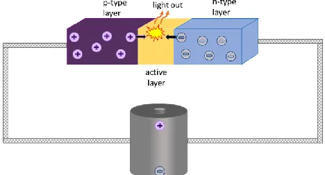
A LED is an electronic device that use electric current pass through it to emit visible light. LED operates in forward bias like a normal pn-junction diode. This process occurs when the charges that carry the electric current which consist of holes in p-type semiconductors and electron in n-type semiconductors combine within a pn-junction in semiconductor materials and release energy in the form of light. In order to use LED device, n-type material must be connected to the negative terminal of the battery and p-type material must be connected to the positive terminal of the battery. Figure 1 is a simple LED pn-junction configuration under forward bias condition.
Figure 1: Schematic of simple forward biased LED p-n junction and LED basic operation when electrons and holes recombined in the active
region to produce photons [5],[6]
[image:3.420.93.327.297.423.2]152
the pn-junction can emits its energy in the form of light. The films of chip LED structure normally grown epitaxially using metal organic chemical vapor deposition (MOCVD) and metal organic vapor phase epitaxy (MOVPE) in high temperature condition. Generally, GaN-based materials are used for n-layer and p-layer. To create the n-type and p-type GaN layers, it was doped using silicon (Si) to obtain n-type GaN layer while magnesium (Mg) to obtain p-type GaN layer. The doping techniques such as thermal annealing, impurity diffusion, ion implantation is able to alter the undoped GaN to have high density of electrons or holes. Another important layer is the active layer where the pn-junction in semiconductor materials releases energy in the form of light. Normally, active layers materials use semiconductors such as gallium arsenide (GaAs), gallium phosphide (GaP), indium gallium nitride (InGaN), aluminum gallium nitride (AlGaN) and aluminum gallium indium nitride (AlGaInN). All these materials have different band gap which capable to emits light in different wavelength ranging from infrared to visible light through until ultraviolet. As for the rest, the substrates also can affect the quality of chip LED. Typically, the substrates in LED chip have a different in lattice mismatch between the substrates and the epitaxial layers. This cause stacking faults and threading dislocations in GaN epilayers [7] and lead to cracking [8] in LED chip. Hence, the substrates of LED chosen normally have close lattice match to the GaN layer. Common substrates are GaN, sapphire (Al2O3), GaAs, Si and silicon carbide (SiC) [8–11].
153
Figure 2: Basic structure of LED chip using InGaN/AlGaN double heterostructure for blue emission LED [6],[13]
Figure 3: Final LED structure type pinned LED. Cross sectional image of an LED packaging. LED chip sits on a reflector cup and is embedded in a transparent epoxy whose shape favors light extraction to air. Combination of LED chip emission pattern, shape of reflector cup and refractive index
[image:5.420.125.294.267.441.2]154
8.3 FABRICATION OF CONVENTIONAL BLUE-LED AND
UV-LED
The conventional LED fabrication for high efficiency blue-light emission in the 90s commonly use hydride vapor phase epitaxy (HVPE), molecular beam epitaxy (MBE) and MOCVD methods to grow the epitaxial layer. All
these methods were using high temperature process up to 1000 ◦C in return
to achieve high quality and solid epitaxial layer. The epitaxial growth of GaN for LED application using MOCVD has been firstly reported by Nakamura, Senoh and Mukai in 1993 [15],[16]. Figure 4 shows schematic diagram of blue-LED by Nakamura, Senoh and Mukai in 1993. It was reported that the
sapphire substrates were heated first to 1050 ◦C in hydrogen stream, then
the GaN buffer layer is grown using 510oC and followed by Si doped n-type
GaN layer using 1020oC in trymethyl-gallium (TMG), SiH4 and NH3
precursor gas. After the GaN layer, the InGaN layer is growth using 800oC
in TMG, NH3 and trymethyl-indium (TMI) working gas. The process
temperature then increased to 1020 ◦C to growth Mg doped p-type GaN.
After the film growth, low energy electron beam irradiation (LEEBI) treatment was performed to obtain highly p-type GaN layer. Finally, the fabrication of LED chip accomplish as gold (Au) contact layer was evaporated to p-type GaN and aluminum (Al) contact onto n-type GaN layer. Prior to the contact pad deposition, a small portion of p-type GaN layer is etched until partially n-type GaN layer was exposed.
[image:6.420.86.324.341.458.2]
Figure 4: Schematic diagram blue-LED by Nakamura, Senoh and Mukai in 1993 [15][16]
155
Most of the fabrication processes, until today, using high temperature and high flow rate working gas.
After the development of blue-LED, ultraviolet-LED (UV-LED) is the latest issue that has been addressed by many researchers. Recent publication in [3] used high temperature for UV-LED chip epitaxial layers. Figure 5 shows the schematic of UV-LED and fabrication method with respective temperature. In brief, the aluminum nitride (AlN) thin films which act as buffer layer were deposited on sapphire substrates using reactive radio frequency magnetron sputtering deposition. Prior to deposition, the
substrate was heated to 600 ◦C. Then, the film was transferred to MOCVD
chamber to grow 20 periods of AlN/Al 0.65 Ga 0.35 N at 1130 ◦C. After
that, a silicon-doped n-type Al 0.56 Ga 0.44 N layer was grown on the
AlN/AlGaN at 1005◦C. Next for the active layer, 5 pairs of AlGaN were
grown followed by Mg doped p-AlGaN and p-GaN. At the end of the
[image:7.420.86.334.266.465.2]process, the structure was annealed at 800 ◦C to activate the Mg acceptor.
Figure 5: Schematic diagram of UV-LED [3]
8.4 FABRICATION OF LED CHIP USING LOW
TEMPERATURES PROCESS
156
between the substrate and GaN epilayers by introducing nucleation layer between the thin films [20]. One of the techniques for growing these group materials at relatively low temperature is using magnetron sputtering deposition. There are three types of sputtering process which are direct current (DC) sputtering, radio frequency (RF) sputtering and high power impulse magnetron sputtering (HiPIMS) [21]. The sputtering process generally produced from the bombardment of target surface with energetic gaseous ions that cause the physical ejection of surface atoms. The number of ejected atoms is depends on the incident energy of ions [22]. Sputtering technique is also applied for ion etching, analytical techniques and thin film deposition. Further details of magnetron sputtering deposition can be found in various reference books [23–27].
8.4.1 LED Chip Fabrication Using Low Temperature Process
Fabrication of LED chip using low temperature is not well established yet and there are several papers reported on the experimental works. To date, researchers are focusing to fabricate a blue-LED using temperature below
1000oC with an output power of 1.5 mW, an equivalent quantum efficiency
(EQE) of 2.7% and 450 nm of emission wavelength, which is the standard specification of commercial LED [2].The main reason of LED chip using high temperature is because of the process of MOCVD itself required high temperature to deposit the precursor gas to grow the epitaxial layer and obtain the solid epitaxial layer. Hence, further studies to improve the technique for fabrication of LED using lower temperature must be established so that LED can be fabricated on a plastic or fabric in the near future.
8.4.2 Low Temperature Blue-LED Produced Using
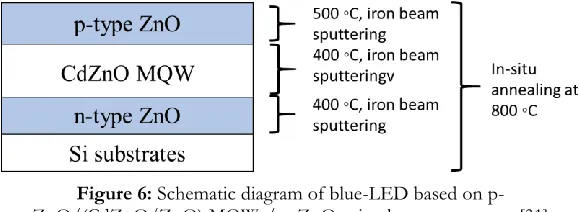
p-ZnO/(CdZnO/ZnO) MQWs/n-ZnO Configuration
There are several reports on deposition of single layer structure for optimization of LED especially for p-type layer and contact layer [28-30] . However, the experimental work on fabrication of the complete LED chip
using all low temperature process which is below than 1000 ◦C is not
reported yet. Recently, blue-LED based using p-ZnO/(CdZnO/ZnO) MQWs/n-ZnO configuration at room temperature using dual ion beam sputtering had been fabricated by [31]. The n-layer structure was made up from Ga-doped ZnO which was deposited on Si substrates by using
substrate temperature of 400 ◦C [32]. After that, two-period cadmium zinc
157
with i-ZnO barrier which is grown using same temperature and method with n-layer structure. Lastly, p-layer structure was deposited on top of the
CdZnO/ZnO MQW at 500◦C using Sb doped ZnO (SZO) target. Each
layer undergoes in-situ annealing process at 800◦C in vacuum to activate
the dopant. To complete the LED as a device, an indium electrode was used as an ohmic contact on n-Si substrate and p-type SZO. The temperature to
form the ohmic contact on both layers is 400◦C in high vacuum condition.
[image:9.420.65.355.195.301.2]The device was observed to emit UV electroluminescent (EL) emission until 442 nm at 130 mA injection current using turn-on voltage of 4.69 V. Figure 6 shows the schematic diagram of their fabrication processes.
Figure 6: Schematic diagram of blue-LED based on p-ZnO/(CdZnO/ZnO) MQWs/ n-ZnO using low temperature [31]
8.4.3 Fabrication of GaN-based LED on Flexible Metal Foils
Recently, H. Kim et. al. performed fabrication of full color GaN based LED diodes on almost lattice-matched flexible hafnium (Hf) metal foils using
pulse sputtering deposition (PSD) in the temperature range of 400-700◦C
[33]. As shown in Figure 7, the n-type GaN layer was deposited on Hf metal
foil at temperature 700 ◦C. Prior to deposition, the Hf metal foil was
annealed at 1000 ◦C for 60 minutes in vacuum to produce highly c-axis
oriented structure. Then, five periods of InGaN/GaN MQW was deposited
and topped by Mg-doped p-type GaN layer all using 400 ◦C. Lastly, In and
158
Figure 7: Schematic diagram of full-color GaN-based LED on nearly lattice-matched flexible hafnium metal foils [33]
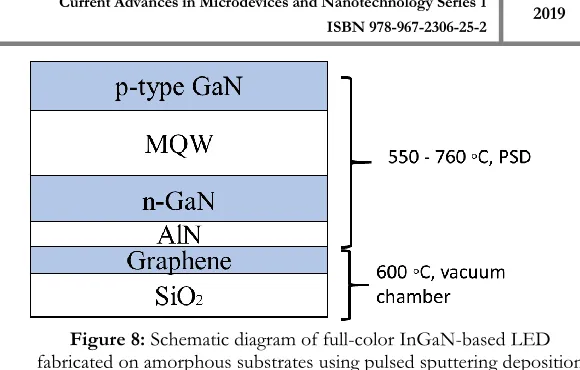
8.4.4 Fabrication of InGaN-based LED on Amorphous Substrates
Fabrication of full-color InGaN-based LED using low temperature process has been presented by J. W. Shon et. al. [4]. The highest temperature used
for the nitrite films in this experiment is only at 760◦C by pulsed sputtering
deposition (PSD) techniques. High crystalline nitride films successfully prepared on amorphous fused silica substrates. It was done by growing the multilayer graphene layers on nickel (Ni) foil using CVD then transferred
onto amorphous fused silica substrates or amorphous SiO2 which was
prepared by thermal oxidation of Si. AlN buffer layer was deposited followed by GaN layer using PSD with a growth rate of 1-2 mm/h to form
n-type layer AlN/graphene/amorphous SiO2 structures. Then, 5 periods of
alternating InGaN/GaN MQW were grown on n-type layer followed by Mg doped p-type GaN layer is grown on the top of MQW, as shown in Figure 8. The nitride layers were deposited at substrate temperatures range
of 550-760 ◦C. To perform electroluminescence measurement on LED
[image:10.420.61.345.33.167.2]159
Figure 8: Schematic diagram of full-color InGaN-based LED fabricated on amorphous substrates using pulsed sputtering deposition
[4]
8.5 SUMMARY
In summary, the basic component of LED that enables it to emit light is the charges that carry the electric current which consist of holes in p-type semiconductors and electron in n-type semiconductors which combine within a pn-junction in semiconductor materials. The fabrication of LED
chip using low temperature below 1000◦C is possible and reliable as the
emission wavelength of LED are 442 nm, 460 nm and 520 nm. The combination of various deposition techniques such as thermal annealing, PSD and electron beam enable to avoid the use of expensive and high temperature techniques when compared to commonly used MOCVD. Hence, these understanding are beneficial to the development of low-cost production and commercial applications for future LED and optoelectronic devices.
ACKNOWLEDGEMENT
This study is partially supported by Ministry of Education Malaysia and Industrial Grant under the contract Vot U675. Nafarizal and Muliana acknowledge the financial support by CREST Sdn. Bhd. through their R&D fund code P28C1-17.
REFERENCES
160
light qualities and their corresponding scientific applications. Renewable and
Sustainable Energy Reviews, 51, 55-61.
[2] Nakamura, S. (2015). Background story of the invention of efficient
blue InGaN light emitting diodes (Nobel Lecture). Annalen Physik, 527
(5-6), 335-349.
[3] Zhao, L., Zhang, S., Zhang, Y., Yan, J., Zhang, L., Ai, Y., Guo, Y.,
Ni, R., Wang, J., and Li, J. (2018). AlGaN-based ultraviolet light-emitting diodes on sputter-deposited AlN templates with epitaxial AlN/AlGaN
superlattices. Superlattices and Microstructures, 113, 713-719.
[4] Shon, J. W., Ohta, J., Ueno, K., Kobayashi, A., and Fujioka, H.
(2014). Fabrication of full-color InGaN-based light-emitting diodes on
amorphous substrates by pulsed sputtering. Scintific Report, 4, 5325.
[5] Feezell, D., and Nakamura, S. (2018). Invention, development, and
status of the blue light-emitting diode, the enabler of solid-state lighting.
Comptes Rendus Physique, 1, 1-21.
[6] Akasaki, I. (2007). Key inventions in the history of nitride-based
blue-LED and LD. Journal of Crystal Growth, 300(1), 2-10.
[7] Saengkaew, P., Sanorpim, S., Yordsri, V., Thanachayanont, C., and
Onabe, K. (2015). Characterization of semi-polar GaN on GaAs substrates.
Journal of Crystal Growth, 411, 76-80.
[8] Hu, J., Zhang, Y., Sun, M., Piedra, D., and Chowdhury, N. (2017).
Materials and processing issues in vertical GaN power electronics. Materials
Science Semiconductor Processing, 78, 1-11.
[9] Liu, L., and Edgar, J. H. (2002). Substrates for gallium nitride
epitaxy. Materials Science Engineering: R Reports, 37 (3), 61-128.
[10] Watson, I. M. (2013). Metal organic vapour phase epitaxy of AlN, GaN, InN and their alloys: A key chemical technology for advanced device
applications. Coordination Chemistry Reviews, 257 (13-14), 2120-2141.
161
[12] Zhang, S. U. (2016) Chip package interaction for LED packages. Microelectronic Reliability, 63, 76-81.
[13] Ryu, H. Y., Jeon, K. S., Kang, M. G., Yuh, H. K., Choi, Y. H. and Lee, J. S. (2017). A comparative study of efficiency droop and internal electric field for InGaN blue lighting-emitting diodes on silicon and
sapphire substrates. Scintifik Report, 7, 44814.
[14] David, A., Benisty, H., and Weisbuch, C. (2012). Photonic crystal
light-emitting sources. Reports on Progress Physics, 75(12), 1-38.
[15] Nakamura, S., Senoh, M., and Mukai, T. (1993).
p-GaN/n-InGaN/n-GaN double-heterostructure blue-light-emitting diodes. Japanese
Journal of Applied Physics, 32, 8–11.
[16] Nakamura, S. and Mukai, T. (1992). High-quality InGaN films
grown on GaN films. Japanese Journal of Applied Physics, 31, 1457-1459.
[17] Iwaya, M., Terao, S., Sano, T., Takanami, S., Ukai, T., Nakamura, S. Kamiyama, R., Amano, H., and Akasaki, I. (2001). High-efficiency GaN/AlxGa1-xN multi-quantum-well light emitter grown on
low-dislocation density AlxGa1-xN, PhysicaStatus Solidi(A) Applied Research, 188
(1), 117-120.
[18] Jayasakthi, M., Juillaguet, S., Peyre, H., Konczewicz, L., Baskar K., and Contreras, S. (2016). Influence of AlN thickness on AlGaN epilayer
grown by MOCVD, Superlattices and Microstructure, 98, 515-521.
[19] Iwaya, M., Terao, S., Sano, T., Ukai, T., Nakamura, R., Kamiyama, S., Amano, H., and Akasaki, I. (2002). Suppression of phase separation of AlGaN during lateral growth and fabrication of high-efficiency UV-LED
on optimized AlGaN. Journal Crystal and Growth, 237, 951-955.
[20] Hu, H., Zhou, S., Liu, X., Gao, Y., Gui, C., and Liu, S. (2017). Effects of GaN/AlGaN/Sputtered AlN nucleation layers on performance
of GaN-based ultraviolet light-emitting diodes. Scientific Report, 7, 44627.
[21] Tian, L., Cheng, G., Zheng, R., Tian, K., Yan, X., Hu Z., and Wang, H. (2017). Effect of sputtering deposition process of indium tin oxynitride
on surface damage of gallium nitride film. Superlattices and Microstructure, 109,
162
[22] Wender, H., Migowski, P., Feil, A. F., Teixeira, S. R., and Dupont, J. (2013). Sputtering deposition of nanoparticles onto liquid substrates:
Recent advances and future trends. Coordination Chemistry Reviews,
257(17-18), 2468–2483.
[23] Wasa, K., Kanno, I., and Kotera, H. (2012). Handbook of sputter deposition technology: fundamentals and applications for functional thin films, Nano-materials and MEMS, Second Edition.
[24] Kiyotaka W., and Hayakawa, S. (1992). Handbook of Sputter Deposition Technology: Principles, Technology, and Applications.
[25] Adachi, H., Hata, T., and Wasa, K. (2012). Basic process of sputtering deposition, in handbook of sputter deposition technology:
fundamentals and applications for functional thin films. Nano-Materials and
MEMS 2, 295-359.
[26] Greene, J. E. (2017). Review article: tracing the recorded history of
thin-film sputter deposition: From the 1800s to 2017. Journal of Vacuum
Science and Technology: A Vacuum, Surfaces, and Films, 35(5), 05C204,
[27] Helmersson, U., Lattemann, M., Bohlmark, J., Ehiasarian, A. P., and Gudmundsson, J. T. (2006). Ionized physical vapor deposition (IPVD): A
review of technology and applications. Thin Solid Films, 513 (1-2), 1-24.
[28] Yohannes, K. and Kuo, D. H. (2015). Growth of p-type Cu-doped
GaN films with magnetron sputtering at and below 400 ◦C. Materials and
Science Semiconductor Process, 29, 288-293.
[29] Hong, C. H., Wie, S. M., Park, M. J., and Kwak, J. S. (2013). Electron beam irradiated ITO films as highly transparent p-type electrodes for
GaN-based LEDs. Journal of Nanoscience and Nanotechnology, 13(8), 5420-5423.
[30] Song, J. O., Ha, J. S. and Seong, T. Y. (2010). Ohmic-contact technology for GaN-based light-emitting diodes: Role of p-type contact.
IEEE Transaction on Electron Devices, 57(1), 42-59.
[31] Awasthi, V., Pandey, S. K., Verma, S., and Mukherjee, S. (2016). Room temperature blue-LED based on p-ZnO/(CdZnO/ZnO) MQWs/
163
[32] Kumar, S., Sushil, P., and Pandey, K. (2013). Investigation of dual
ion beam sputtered transparent conductive Ga-doped ZnO films. Journal of
Materials Science: Materials in Electronic, 24 (12), 4919-4924.
[33] Kim, H., Ohta, J., Ueno, K., Kobayashi, A., Morita, M, Tokumoto, Y., and Fujioka, H. (2017). Fabrication of full-color GaN-based
light-emitting diodes on nearly lattice-matched flexible metal foils. Scientific
![Figure 2: Basic structure of LED chip using InGaN/AlGaN double heterostructure for blue emission LED [6],[13]](https://thumb-us.123doks.com/thumbv2/123dok_us/8750208.891721/5.420.125.294.267.441/figure-basic-structure-ingan-algan-double-heterostructure-emission.webp)
![Figure 4: Schematic diagram blue-LED by Nakamura, Senoh and Mukai in 1993 [15][16]](https://thumb-us.123doks.com/thumbv2/123dok_us/8750208.891721/6.420.86.324.341.458/figure-schematic-diagram-blue-led-nakamura-senoh-mukai.webp)
![Figure 5: Schematic diagram of UV-LED [3]](https://thumb-us.123doks.com/thumbv2/123dok_us/8750208.891721/7.420.86.334.266.465/figure-schematic-diagram-of-uv-led.webp)
![Figure 7: Schematic diagram of full-color GaN-based LED on nearly lattice-matched flexible hafnium metal foils [33]](https://thumb-us.123doks.com/thumbv2/123dok_us/8750208.891721/10.420.61.345.33.167/figure-schematic-diagram-nearly-lattice-matched-flexible-hafnium.webp)