© 2016, IRJET | Impact Factor value: 4.45 | ISO 9001:2008 Certified Journal
| Page 382
A Novel Snubberless DC-DC Converter Based Inverter
Soumya Beegam.A
1, Asha M.A
21
Soumya Beegam. A, Student, Dept.of Electrical and Electronics Engineering, KMEA Engineering
College,Edathala,Kerala,India
2
Asha M.A, Assistant Proffessor, Dept.of Electrical and Electronics Engineering, KMEA Engineering
College,Edathala,Kerala,India
---***---Abstract -
The project deals with a snubberless dc/dcconverter-based inverter. Most of the dc-dc converters, which require snubber circuits for reduce voltage spikes. In the case of conventional dc-dc converters, during device turn-off, voltage overshoot occurs across the various semiconductor devices. So, an additional snubber circuit or voltage clamping is required to limit the overshoot voltage. It increases the components count and losses making the converter less efficient. The above problem is eliminated by operating the converter with soft-switching features achieved by using secondary modulation technique. Hence, it avoids the need of additional snubber. In this topology having Zero Voltage Switching (ZVS) and Zero Current Switching (ZCS) features. The switches in the converter turn ON at ZVS and turn OFF at ZCS . The proposed converter is a converter with high-step-up voltage conversion ratio. Then the output from the dc-dc converter is connected to full bridge inverter. Inverter produces ac which is connected to grid/load. These types of snubberless dc/dc converter based inverters are mainly used for residential photovoltaic (PV) applications, fuel cell vehicles and energy storage systems. The designed system has been simulated using Simulink Model (Matlab-Software) tools.
Key Words: Snubberless dc-dc converter, Soft Switching, Zero Voltage Switching, Zero Current Switching, Secondary modulation Technique
1.INTRODUCTION
In the year 2006, the author Lizhi Zhu highlights on a novel soft-commutating isolated boost full-bridge ZVS-Pulse Width Modulation (PWM) dc–dc converter for bidirectional high power applications [1].A soft-commutating and control method for an isolated boost full bridge converter is proposed for dual operation of the well-known soft-switching full bridge dc/dc buck converter. It provides unique commutation logic to minimize a mismatch between current in the current-fed inductor and current in the leakage inductance of the transformer when commutation occur, significantly reducing the power rating for a voltage clamping snubber and allow use of a simple passive clamped snubber. To minimize the mismatch, the method and control
scheme utilizes the resonant tank and freewheeling path in the existing full bridge inverter at the voltage-fed side. It is used to preset the current in the leakage inductance of the transformer in a resonant manner. Zero-voltage-switching is also achieved for all the switches at the voltage-fed side inverter in boost mode operation. The soft-commutating method is verified through boost mode operation of a 3-kW bidirectional isolated full bridge dc/dc converter implemented for fuel cell electric vehicle applications. In the year 2008, the authors Alexander Isurin et al. emphasis on soft switching passive snubber circuit with energy recovery [2].It uses only passive components, and it has energy recovery to the source. Most commonly, a minimum of 70-80% of the energy is used for the controlling the power switch “load line” would be returned to the source.
The snubber circuit is suitable for use in full leg power conversionIn the year 2010, the authors Tsai-Fu Wu et al. highlights on isolated bidirectional full-bridge dc–dc converter with a fly-back snubber [3].An isolated bidirectional full-bridge dc–dc converter with high conversion ratio, high output power, and soft start-up capability was proposed. The flyback snubber can alleviate the voltage spikes due to current difference between the current-fed inductor and leakage inductance of the isolation transformer, and can reduce the current flowing through the active switches at the current-fed side by 50%. Therefore, the current does not circulate through the full-bridge switches, their current stresses can be reduced under heavy-load condition, so improving system reliability significantly. The flyback snubber can be also controlled to achieve a soft start-up feature.
The authors Tsai-Fu Wu, Jeng-Gung Yang and Chia-Ling Kuo proposed Soft-switching bidirectional isolated full bridge converter with active & passive snubber [4].This topology presented a soft-switching bidirectional isolated full-bridge converter, which allows input voltage variation from 42V to 54V, for battery charging/discharging applications.
Soft-switching current-fed half-bridge front-end isolated DC-DC converter based inverter for AC module applications was
© 2016, IRJET | Impact Factor value: 4.45 | ISO 9001:2008 Certified Journal
| Page 383
has been proposed for PV applications, addressing highefficiency, good integration level, galvanic isolation, flexibility toward the source, and reliability. The converters achieve clamping of the device voltage by secondary modulation, thus eliminating the need of snubber or active clamp circuits. This topology is used as a reference for understanding the benefits of soft-switching and the method of attaining it.
The authors Rong-Jong Wai et al. emphasis on a high
efficiency bidirectional converter for power sources with great voltage diversity [6]. This paper is used as a reference for mitigating the switching losses by using transformer based circuit topologies and frequently applying soft switching techniques including zero voltage switching (ZVS)
or zero current switching (ZCS). Unfortunately, switches of
four and upward in these transformer-based topology increases production costs and reduce conversion efficiency. In this study, a coupled-inductor bidirectional converter scheme utilizes only three power switches to fulfil the objective of bidirectional current control. The high step-up and step-down ratios enable a battery module with a low voltage to be injected into a high-voltage dc bus for subsequent utilization. The techniques of voltage clamping, synchronous rectification and soft switching are exploited thus providing high efficiency bidirectional power conversion for power sources with large voltage diversity.
Zero voltage transition PWM three level boost converters for power factor pre-regulator were proposed. The benefit is using one auxiliary switch in active soft switching circuit. This topology is used as a reference for achieving zero voltage turn-on and zero voltage turn-offs of the main switches and also reducing the reverse recovery loss of boost diode. In addition the auxiliary switch achieves ZCS during turn-on switching transition thus featuring the effectiveness of the converter. [7]
In the year 2004, the authors R. Gopinath et al. emphasis on
active-clamping zero-voltage switching PWM current-fed half-bridge converter current-fed half-bridge isolated dc to dc converter [8]. An active-clamp helps in achieving soft switching features of devices and absorbs the turn-off voltage spike across the switches. Therefore, an active clamp dissipates around 1% of the output power. In addition, it increases the current stresses across the components and introduces circulating current that leads to higher switch rms current. It requires two additional active switches, two snubber capacitors, and one High-Frequency (HF) capacitor of large value, this will increases the component count and converter complexity. Voltage across the switches is clamped without an active clamp or passive snubber circuits. It makes a reduction in size and cost of the system. It improves the converter efficiency by ZCS of primary devices, zero-current turn-on of all devices, and natural commutation of secondary diodes and body diodes of primary devices. Switching transition losses are significantly reduced.
In the year 2010, snubberless bidirectional dc–dc converter with new CLLC resonant tank featuring minimized switching loss [9] was proposed by the authors Wei Chen, Ping Rong, and Zhengyu Lu. A bidirectional dc–dc converter (BDC) with a new CLLC-type resonant tank, which features zero-voltage switching (ZVS) for the input inverting choppers and zero-current switching (ZCS) for the output rectifier switches, is proposed in this paper. This converter has a minimized switching loss if all of the main switches are implemented with metal–oxide–semiconductor field-effect transistors, and thereby, the proposed converter is fully soft switched and snubberless. The detail operation principles, as well as the design considerations, are presented. The methodologies to develop a unidirectional ZVS+ZCS dc–dc converter for the corresponding pulse-width modulation and frequency modulation converters are proposed. In 2013, the authors Akshay K. Rathore et al. highlight on snubberless bidirectional naturally clamped ZCS/ZVS current-fed half-bridge dc/dc converter [10] for fuel cell vehicles. This paper presents a snubberless naturally clamped bidirectional current-fed half-bridge isolated dc/dc converter for fuel cell vehicles (FCVs). The proposed converter achieves zero-current switching (ZCS) of the primary-side active semiconductor devices and zero-voltage switching of the secondary-side active semiconductor devices. It is a potential topology for fuel cell vehicles, front-end dc/dc power conversion for fuel cell inverters, and energy storage. A proposed secondary-modulation clamps the voltage across the primary-side devices naturally and eliminates switch turn-off voltage spike concern with ZCS without any additional circuit. This leads to lower cost. Voltage across the primary-side current fed devices is independent of duty cycle like conventional current-fed converters but clamped at a reflected output voltage. Hence, comparatively low-voltage-rating devices with a low ON-state resistance are used, introducing low conduction losses and higher efficiency.
© 2016, IRJET | Impact Factor value: 4.45 | ISO 9001:2008 Certified Journal
| Page 384
voltage and current ratings, better thermal distribution areobtained.
In the year 2014, the authors Pan Xuewei et al. highlights on soft-switching snubberless naturally clamped current-fed full-bridge front-end-converter [13]. A novel naturally clamped zero-current commutated soft-switching bidirectional current-fed full-bridge isolated dc/dc converter is proposed. This proposed secondary-modulation technique naturally clamps the voltage across the primary-side devices with zero-current commutation, eliminating the necessity for active-clamp circuit or passive snubbers. Switching losses are reduced by zero-current switching of primary side devices and zero-voltage switching of secondary-side devices. Soft switching and voltage clamping are inherent and load independent. The voltage across primary-side devices are independent of duty cycle with varying input voltage and output power and clamped at rather low reflected output voltage, enabling the use of semiconductor devices of low voltage rating. These merits make the converter for fuel cell vehicles application, front-end dc/dc power conversion for fuel cell inverters, and energy storage purposes.
In the year 2013, the authors Udupi R. Prasanna and Akshay K. Rathore proposed novel soft-switching snubberless current-fed half-bridge front-end converter-based PV inverter [12]. This proposes a new novel snubberless current fed half-bridge front-end isolated dc/dc converter-based inverter mainly for photovoltaic applications. It is suitable for grid-tied (utility interface) as well as off-grid (standalone) application. The proposed converter attains clamping of the device voltage by secondary modulation, thus eliminating the need of snubber or active-clamp. Zero-current switching or natural commutation of primary devices and zero-voltage switching of secondary devices is achieved.
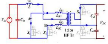
The DC/DC converters are widely used in different types of electronic devices such as battery charger, electric vehicles, and in portable devices like cellular phones, laptops, computers etc. In the case of battery charger applications, after the battery is fully charged, the load is zero and the converter should be safely operate from no-load to full load conditions. The fundamental problem regarding the conventional full bridge DC/DC converter topology is the voltage spikes across output diodes due to transformer leakage inductance and the conventional topology is not able to ensure Zero Voltage Switching (ZVS) operation for wide range of load variations. So a snubberless current-fed full-bridge DC to DC converter topology is introduced in order to reduce the voltage stress arising in the conventional current-fed full-bridge converter and achieving soft switching features.
1.1
Proposed System
The snubberless dc/dc converter [14] used to provide a dc-dc converter with high step-up conversion ratio, low cost and high efficiency. The boost converter is the preferred choice in earlier days because of its high voltage gain and simple circuit design. But the power level is limited due to hard switching operation,it will increases switching losses leading to less efficiency. To increase the power level, power device parallel technology is one of the solutions. Therefore, this method cannot reduce the input and output current ripples. Interleaved structure is another effective solution to increase the power level which can minimize the current ripple, can reduce passive component size, can reduce the passive component size, improve the transient response and can realize the thermal distribution. However, the power devices operate at hard switching leading to less efficiency.
The aim of this project is to achieve soft switching of all semiconductor devices. A novel secondary modulation technique is proposed to naturally clamp the voltage and therefore eliminates the necessity for snubbers. Switching losses are reduced significantly by using Zero- Current Switching (ZCS) and Zero-Voltage Switching (ZVS). Soft switching is inherent, load independent, and is maintained with wide variation of input voltage and power, and it is suitable for PV applications. The boost converter is used in conjunction with a high frequency transformer to boost the output voltage with the advantage of providing isolation between the input and output stage. Without extreme duty cycle and high switch voltage stress that exists in the conventional boost converter the proposed converter achieves high step-up conversion ratio, low cost, and high efficiency etc.
1.2 Operation of the proposed system
In this section, steady-state operation and analysis of proposed high step-up dc-dc converter have been explained. To simplify the analysis of the proposed system, the following assumptions are made:
1) Boost inductor L is large enough to maintain constant current through it.
2) All the components are ideal.
3) Series inductors Llk1 and Llk2 include the leakage
inductances of the transformer. The total value of Llk1 and Llk2 is represented as Llk_T.
4) Magnetizing inductance of the transformer is infinitely large.
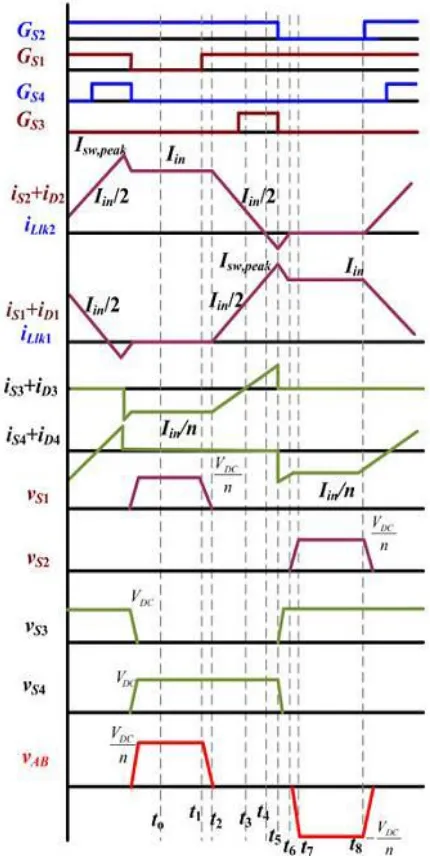
The steady-state operating waveforms are the primary switches S1 and S2 are operated with identical gating signals
© 2016, IRJET | Impact Factor value: 4.45 | ISO 9001:2008 Certified Journal
| Page 385
MODE 1 (to < t < t1)In the first mode, primary side switch S2 and anti-parallel
body diode D3 of the secondary side switch are conducting. Power is transferred to the load through HF transformer in the system. The non-conducting secondary device S4 is
blocking output voltage VDC and primary device S1 is
blocking reflected output voltage VDC/n. The values of
current through various components are: iS1 =0, iS2 =Iin , iLlk1=0, iLlk2= Iin, iD3 = Iin/n. Voltage across the switch S1:
[image:4.595.310.525.102.530.2]VS1 = VDC/n. Voltage across the switch S4: VS4 = VDC.
Fig -1: Mode 1
MODE 2 (t1 < t < t2)
At t=t1, primary switch S1 is turned-on. Then the capacitor C1 discharges in a very short period of time. At the end of
this interval, S1 is fully conducting and C1 is completely
discharged.
Fig -2: Mode 2
Fig -3: Operating waveforms of the proposed system MODE 3 (t2 < t < t3)
In this mode, all two primary switches S1 and S2 are
conducting. Reflected output voltage appears across series inductors Llk1 and Llk2, diverting/transferring the current from switch S2 to S1. It causes current through previously
conducting device S2 to reduce linearly. It results in
conduction of switch S1 with zero current which helps
reducing turn-on losses. Before the end of this interval, the body diode D3 is conducting. Hence, S3 can be gated on for ZVS turn-ON. At the end of this interval, D3 commutates
naturally. Then, the current through all primary devices reaches Iin/2. Then final values are: iLlk1= iLlk2=Iin/2, iS1= iS2
[image:4.595.38.280.242.377.2]© 2016, IRJET | Impact Factor value: 4.45 | ISO 9001:2008 Certified Journal
| Page 386
Fig -4: Mode 3MODE 4 (t3 < t < t4)
In mode 4, secondary side switch S3 is turned-on with zero voltage switching. Currents through all the switching devices continue increasing or decreasing with the same slope as interval 3. At the end of this interval, the primary side switch S2 commutates naturally with Zero Current Commutation
[image:5.595.37.266.373.467.2](ZCS). Then the corresponding current iS2 reaches zero obtaining ZCS. The full current, i.e. input current is taken over by other device S1. The final values are: iLlk1=iS1 =Iin, iLlk2=iS2 =0, iS3 = Iin/n.
Fig -5: Mode 4
MODE 5 (t4 < t < t5)
In this interval, the leakage inductance current iLlk1
increases further with the same slope and anti-parallel body diode D2 starts conducting causing extended zero voltage to
appear across commutated switch S2 to ensure ZCS turn-off. Now, the secondary device S3 is turned-off. At the end of this
[image:5.595.307.543.374.481.2]interval 5, current through switch S1 reaches its peak value.
Fig -6: Mode 5
MODE 6 (t5 < t < t6)
During mode6, secondary side switch S3 is turned-off.
Anti-parallel body diode of switch S4 (ie, D4) takes over the
current immediately. Therefore, the voltage across the transformer primary reverses its polarity. The current through the switch S1 and body diodes D2 also start
decreasing. At the end of this interval, current through D2
[image:5.595.312.548.610.718.2]reduce to zero and is commutated naturally. Current through S1 reaches input current Iin.
Fig -7: Mode 6
MODE 7 (t6 < t < t7)
In this mode, capacitor C2 charges to VDC/n within a short
period of time.Now ,switch S2 is in forward blocking mode.
Fig -8: Mode 7
MODE 8 (t7 < t < t8)
In this interval, currents through S1 and transformer are constant at input current Iin. Current through anti-parallel
body diode of the secondary switch D4 is reaches at Iin/n.
The final values are: iLlk1=iS1 =Iin, iLlk2=iS2 =0, iD4 = Iin/n.
Voltage across the switch S2, VS2 = VDC/n. In this mode
current has transferred from switch S2 to S1, and the transformer current has reversed its polarity.
[image:5.595.35.275.611.710.2]© 2016, IRJET | Impact Factor value: 4.45 | ISO 9001:2008 Certified Journal
| Page 387
2. SIMULATION RESULTS
[image:6.595.50.293.187.373.2]The simulink model of proposed system is shown below. It consists of pulse generation section, dc-dc converter section and full-bridge inverter section.
Fig -10: Simulink Model of Proposed System
The pulses for switches S1, S2, S3 and S4 are generated by
Pulse Width Modulation (PWM) technique. In this PWM signals produced by comparing triangular carrier wave with duty cycle ratio and giving corresponding delay for each switches. The switching frequency of carrier wave is 10 kHz
.
[image:6.595.308.552.283.452.2]Fig -11: Switching Pulses of dc-dc Converter
[image:6.595.50.269.483.657.2]Fig -12: Snubberless DC-DC Converter output for 12V input
Fig -13: Full Bridge output for 12V input
3. CONCLUSION
The proposed snubberless dc/dc converter based inverter can be used to achieve soft switching features. In most of the dc-dc converter based inverter consists of snubber circuits. But it will bring extra losses resulting in low efficiency, owing to circulating current and high ON-state resistance devices. Also, additional components increase the volume and cost of the system. Therefore, the modulation technique used in the proposed system is secondary modulation. The secondary modulation can be used to achieve soft switching features (Zero Current and Zero Voltage Switching) and eliminating the need of snubber circuits in dc-dc converters, making it novel and snubberless.
© 2016, IRJET | Impact Factor value: 4.45 | ISO 9001:2008 Certified Journal
| Page 388
These types of snubberless dc/dc converter based invertersare mainly used for residential photovoltaic (PV) applications, fuel cell vehicles and energy storage systems. The designed system has been simulated using Simulink Model (Matlab-Software) tools.
REFERENCES
[1] L. Zhu, “A novel soft-commutating isolated boost full-bridge ZVS-PWM DC–DC converter for bi-directional high power applications,” IEEE Trans. Power Electron., vol. 21, no. 2, pp. 422–429, Mar. 2006.
[2] Alexander Isurin and Alexander Cook “soft switching passive snubber circuit with energy recovery” IEEETrans. Power Electron., vol. 23, no. 8, pp. 465–468, Feb. 2008.
[3] Tsai-Fu Wu ,Yung-Chu Chen and Jeng-Gung Yang “ isolated bidirectional full-bridge dc–dc converter with a flyback snubber” IEEETrans. Ind. Electron., vol. 25, no. 7, pp. 555–560, September 2010 [4] Tsai-Fu Wu ,Jeng-Gung Yang and Chia-Ling Kuo
“Soft-switching bidirectional isolated full bridge converter with active & passive snubber” IEEE Trans. Power Electron., vol. 16, no. 3, pp. 293–300, March 2014.
[5] S. J. Young, S. C. Shin, J. H. Lee, Y. C. Jung and C. Y. Won, “Soft-switching current-fed push-pull converter for 250-W AC module applications,” IEEE Trans. Power Electron., vol. 29, no. 2, pp. 863-872, Feb 2014.
[6] R. J. Wai and R. Y. Duan, “High-efficiency bidirectional converter for power sources with great voltage diversity,” IEEE Trans. Power Electron., vol. 22, no. 5, pp. 1986–1996, Sep. 2007.
[7] G. Yao, Y. Deng, and X. He, “A ZVT PWM three level boost converter for power factor pre-regulator,” in Proc. IEEE 37th Power Electron. Spec. Conf., 2006, pp. 1–5. Aug. 2006.
[8] S. Han, H. Yoon, G. Moon, M. Youn, Y. Kim, and K. Lee, “A new active-clamping zero-voltage switching PWM current-fed half-bridge converter,” IEEE Trans. Power Electron., vol. 20, no. 6, pp. 1271–1279, Nov. 2005.
[9] W. Chen, P. Rong, and Z. Lu, “Snubberless bidirectional dc–dc converter with new CLLC resonant tank featuring minimized switching loss,”
IEEETrans. Ind. Electron., vol. 57, no. 9, pp. 3075– 3086, Sep. 2010.
[10] Akshay K. RathoreA, and Prasanna U R, “Analysis, Design, and Experimental Results of Novel Snubberless Bidirectional Naturally Clamped ZCS/ZVS Current-Fed Half-Bridge DC/DC Converter for Fuel Cell Vehicles” IEEETrans. Ind. Electron., vol. 60, no. 10, pp. 673–682, Jan. 2013.
[11] Pan Xueweiand Akshay K. Rathore “ interleaved soft-switching bidirectional current-fed full-bridge
isolated voltage doubler is for Fuel Cell Vehicle (FCV) application”, IEEE Trans. Power Electron vol. 28, no. 12, december 2013
[12] Udupi R. Prasanna, Akshay K. Rathore, and Sudip K. Mazumder “novel zero-switching current-fed half-bridge isolated dc/dc converter for fuel-cell-based applications” IEEE Trans. Power Electron., vol.49, no. 4, pp. july/august. 2013.
[13] Udupi R. Prasanna, and Akshay K. Rathore, “analysis, design, and experimental results of a novel soft-switching snubberless current-fed half-bridge front-end converter-based pv inverter” IEEE Trans. Power Electron., vol.28, no. 7, pp. july 2013 [14] Pan Xuewei and Akshay K. Rathore “novel
bidirectional snubberless naturally commutated soft-switching current-fed full-bridge isolated dc/dc converter for fuel cell vehicles” IEEE Trans. Power Electron., vol.61, no. 5, pp.920-925,may 2014. [15] Pan Xuewei , Udupi R. Prasanna and Akshay K.
Rathore “novel soft-switching snubberless naturally clamped current-fed full-bridge front-end-converter-based bidirectional inverter for renewables, microgrid, and ups applications” IEEE Trans. Power Electron., vol.50, no. 6, pp.945-951,November/december 2014.
BIOGRAPHIES
Soumya Beegam.A pursuing
M.Tech in EEE with the specialization of Power Electronics from KMEA Engineering College, Edathala, Aluva, kerala and received B.Tech degree in EEE from Indira Gandhi Institute of Engineering and Technology for Women, Kothamangalam, Kerala in the year 2014. Her interested areas are power electronic converters, multilevel inverters, and renewable energy sources based studies.