http://dx.doi.org/10.4236/cs.2016.75046
Multifunction Filter Employing Current
Differencing Buffered Amplifier
Tajinder Singh Arora, Udit Rana
Department of Electronics and Communication Engineering, Maharaja Surajmal Institute of Technology, New Delhi, India
Received 11 February 2016; accepted 26 April 2016; published 29 April 2016
Copyright © 2016 by authors and Scientific Research Publishing Inc.
This work is licensed under the Creative Commons Attribution International License (CC BY).
http://creativecommons.org/licenses/by/4.0/
Abstract
This paper proposes a new filter biquad circuit, which utilizes three Current Differencing Buffered Amplifiers (CDBA), two capacitors and five resistors, and operates in the trans-resistance mode. This multi-input and single-output multifunction filter uses only grounded capacitors. All the em-ployed resistors are either grounded or virtually grounded, which is an important parameter for its implementation as an integrated circuit. The circuit enjoys independent tunability of angular frequency and bandwidth. The 0.5 µm technology process parameters have been utilized to test and verify the performance characteristics of the circuit using PSPICE. The non-ideal analysis and sensitivity analysis, transient response, Monte-Carlo analysis and calculations of total harmonic distortion have also been shown.
Keywords
Active Filters, Current Differencing Buffered Amplifier, Biquadratic Filter, KHN-Biquad
1. Introduction
KHN filter circuit are mutually independent to each other. Depending upon the type of the active building block used, for the summer and the integrator circuits, various KHN equivalent biquad circuits have been proposed in the literature, some of the prominent reference are [2] [3].
The Current Differencing Buffered Amplifier (CDBA) is an active device which was incepted by C. Acar and S. Ozoguz in 1999 [4]. The main feature of CDBA includes the absence of parasitic capacitance, high slew rate, wide bandwidth, and the ease of its implementation. The presence of a unity-gain voltage amplifier and a unity- gain current differencing amplifier makes it suitable for current and voltage mode signal processing applications e.g. filters, oscillators etc. Various current mode and voltage mode multipurpose filters using CDBA have been reported in literature [5] [6] and cited therein.
In [7] introduced filter circuit has used a large number of passive components. In [8] [9] realized filter with minimal active devices i.e. one only but suffers from the drawback of utilizing floating passive components. Biquadratic filter realization with 3 active devices [10] but has the limitations of use of floating capacitors. A new multifunction biquad using CDBA, has been proposed by taking into consideration of all the said properties of the active building block i.e. CDBA. The proposed circuit employs three CDBAs, two grounded capacitors, one grounded and four virtually grounded resistors. This SIMO circuit operates in the TR mode and has inde- pendent tunability of ω0 and 0
Q
ω
.
In this paper, Section 2 gives the introduction to the active building block i.e. CDBA. Section 3 gives the block diagram and transfer functions of the proposed circuit. In Section 4, the non-ideal analysis of current dif-ferencing buffered amplifier is discussed. Section 5 presents the sensitivity analysis of the proposed filter. Sec-tion 6 demonstrates the simulaSec-tion results of the introduced biquad circuit carried out with the help of PSPICE. At last the concluding remarks have been given in Section 7.
2. CDBA—An Introduction
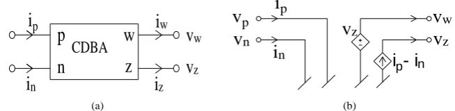
In Figure 1(a), the symbolic representation of the CDBA has been shown, where p and n are the input ports and
w and z are output ports.
The relationship between the input and the output port relationship is given in Equation (1).
0 0 1 1
1 0 0 0
0 0 0 0
0 0 0 0
z
z
w w
p p
n n
i v
v i
v i
v i
−
=
(1)
On solving Equation (1) we get the following device equation
0, 0, , .
p n z p n w z
v = v = i = −i i v =v (2) The p-terminal is the positive (non-inverting) input and the n-terminal is the negative (inverting) input. As per the device Equation (2) and the equivalent circuit given in Figure 1(b), it can be seen that the difference of the currents through the p and the n terminal flows through the z-terminal, as a consequence the z-terminal is also called the current output. The input terminals p and n through which the input current flows are both internally grounded. The voltage generated at the z terminal through an external resistor is copied to the w terminal of the device. The implementation of the CDBA can also be done with the help of CMOS transistors, discussed in Sec-tion 6.
[image:2.595.147.474.625.705.2]
(a) (b)
Figure 1.(a) Systematic device symbol of CDBA; (b) An ideal circuit of the CDBA device.
p
n
w
z
v
wv
zi
pi
ni
zi
wCDBA
v
pv
nv
wv
zv
zi
p- in
i
n3. Proposed Circuit
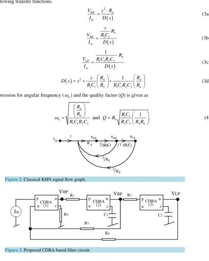
The proposed multi-function biquad diagram is shown in Figure 3. This circuit was designed and develops by using the classical signal-flow graph [3] that has been redrawn in Figure 2 and then converting this signal flow graph into the circuit equation using the characteristic equations of the CDBA. It is clearly seen fromFigure 3 that the proposed configuration has single-input and multiple-outputs, which has the feature that it can be used in a situation where all the three filter responses i.e. High-Pass (HP), Band-Pass (BP) and Low-Pass (LP) are required simultaneously. The proposed circuit can also be converted to VM configuration by simply replacing a voltage source with a series resistance to the input current source. Quality factor (Q) of the circuit can be tuned independently with the help of resistance R5 that does not affect the value of the natural angular frequency (ω0).
By using the terminal relationship given in Equation (2) on the proposed filter circuit given inFigure 3 we get the following transfer functions.
( )
24
HP
in
V s R
I D s
⋅
= (3a)
( )
4 1 1 BP in s R V R CI = D s (3b)
( )
41 1 2 2
1
LP in
R V R C R C
I D s
⋅
= (3c)
( )
2 4 41 1 5 1 1 2 2 6
1
R R
s
D s s
R C R R C R C R
= + +
(3d)
The expression for angular frequency (ω0) and the quality factor (Q) is given as
4
6 1 1
0 5
1 1 2 2 2 2 4 6
1
and .
R
R R C
Q R
R C R C R C R R
ω
= =
(4)
[image:3.595.127.536.227.738.2]Figure 2. Classical KHN signal flow graph.
Figure 3.Proposed CDBA based filter circuit.
1 I v -1 -1 1 1 R in
/
/
/
R R RS C11
/
SR2C25 6 HP 4 vBP vLP p n w z
p p w
z z w n n Iin CDBA (1) CDBA
(2) CDBA(3)
R1
R4
R5
R6
R2
C1 C2
It is clearly visible from Equation (3) and Equation (4) that all the three basic filter responses, namely High- Pass (HP), Band-Pass (BP) and Low-Pass (LP) can easily be realized using the proposed filter configuration. These three are the basic filter responses that may be required from any of the designed filter. As can be seen from the equations that ω0 and the bandwidth 0
Q
ω
has independent tunability. It can also be seen from
Eq-uation (4) that Q is independently tunable and its value can be changed by varying the value of R5. Simulation results based on the same is given in Section 6.
4. Non-Ideal Analysis
For a non-ideal CDBA, the current and voltage tracking errors emanating from the active elements can have a serious impact on the circuit behavior. Thus it is important to take into account the effect of the non-idealities on the circuit performance. On including the non-idealities, the CDBA is characterized by
0 0
0 0 0
0 0 0 0
0 0 0 0
z z
w w
p p
n n
i v
v i
v i
v i
α β
δ
−
=
(5)
, , 0, 0.
z p n w z p n
i =αi −βi v =δv v = v = (6) By applying the terminal relationship given in Equation (6) on the proposed multifunction filter given in Fig-ure 3 we get the following transfer functions.
( )
24 1
HP
in
V s R
I D s
δ
⋅
= (7a)
( )
4 1 2 1 2
1 1
BP in
s R V R C
I D s
α α δ δ
= (7b)
( )
4 1 2 3 1 2 3
1 1 2 2
1
LP in
R V R C R C
I D s
α α α δ δ δ ⋅
= (7c)
( )
2 4 41 1 5 1 1 2 2 6
1
R R
s
D s s
R C R R C R C R
= + +
(7d)
From (7d) we get the values of
ω
0 non-ideal( ) and Q(non-ideal) as( ) ( ) 2 3 1 1 2 3
0 non-ideal 0 ideal
ω =ω α α β δ δ δ (8a)
(non-ideal) (ideal) 3 3 2 1 1 2
.
Q Q
α δ
α β δ δ
= (8b)
From (8a), it can be observed that
ω
0 ideal( ) andω
0 non-ideal( ) differ by a factor which is close to unity. Similarly (ideal)Q and Q(non-ideal) are very close to each other.
5. Sensitivity Analysis
For the proposed circuit the sensitivity analysis, by neglecting the non-idealities of the active device i.e. CDBA is given in Equation (9)
0 0
1, 2, 6,1, 2 4 1 2
R R R C C R
5 1
Q R
S = (9b)
2, 4, 6 1, 1 1
. 2
Q Q
R R R R C
S = −S = − (9c) By considering the non-idealities as given in Equation (5), we have calculated the active sensitivities of the introduced circuit and it has given in Equation (10).
non-ideal 2 3 1 1 2 3
1 2
Sα α β δ δ δω = (10a)
2 1 1 2 2 3 1 2
Q Q
Sα β δ δ =Sα δ = (10b)
non-ideal non-ideal
2 1 1 2 2 3
1 2
Q Q
Sα β δ δ = −Sα δ = − (10c) By close inspection of Equations (9) and Equation (10), one may find that the absolute value of ω0 and Q
sensitivities are within unity. As a result the circuit will exhibit low sensitivity performance.
6. Simulation Results
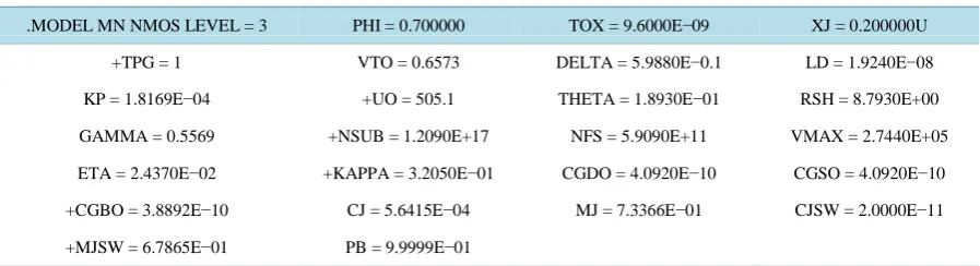
For testing the workability of TR-mode response of the proposed circuit configuration ofFigure 3 on PSPICE the ideal CDBA of Figure 1(b) and the MOS CDBA [11] were employed. The MOS CDBA of [11] has been redrawn here as shown in Figure 4, where all MOS devices operate in saturation. The aspect ratios (W/L) uti-lized for MOSFETs of Figure 4 are 20 µm/1µm and MOS parameters used in the simulations are given in Table 1.
The proposed biquad is designed to operate at 10 MHz and the component values are chosen as R1=10 K, 2 20 K
R = , R4 =10 K, R5 =10 K, R6=10 K, C1 =1.125 pF and C2=1.125 pF. The supply voltages used are +VDD = −VSS = 1.25 V and the constant bias currents IB=30 Aµ are used. The various performance
[image:5.595.116.538.438.720.2]re-sults based on PSPICE simulation are shown inFigures 5-9. The simulation results of low pass, band pass,
[image:5.595.90.539.597.719.2]Figure 4. N-MOS based CDBA [11].
Table 1. 0.5 µm MOS process parameters utilized in simulation.
.MODEL MN NMOS LEVEL = 3 PHI = 0.700000 TOX = 9.6000E−09 XJ = 0.200000U
+TPG = 1 VTO = 0.6573 DELTA = 5.9880E−0.1 LD = 1.9240E−08
KP = 1.8169E−04 +UO = 505.1 THETA = 1.8930E−01 RSH = 8.7930E+00
GAMMA = 0.5569 +NSUB = 1.2090E+17 NFS = 5.9090E+11 VMAX = 2.7440E+05
ETA = 2.4370E−02 +KAPPA = 3.2050E−01 CGDO = 4.0920E−10 CGSO = 4.0920E−10 +CGBO = 3.8892E−10 CJ = 5.6415E−04 MJ = 7.3366E−01 CJSW = 2.0000E−11 +MJSW = 6.7865E−01 PB = 9.9999E−01
2IB
M13
w
IZ
-Vss
p
ip
n
in
+VDD
z
2IB
IB IB IB IB IB
M14
M12
M11
M15
IB
M5
M8
M10
M9
M7
M'5
M'2
M2
M3
M4
M6
M1
M'4
M'1
Figure 5. Ideal and non-ideal frequency response of the proposed multifunction filter circuit.
Figure 6.Variation in Q for different values of R5, while keeping fixed ω0 (10 MHz) for bandpass filter.
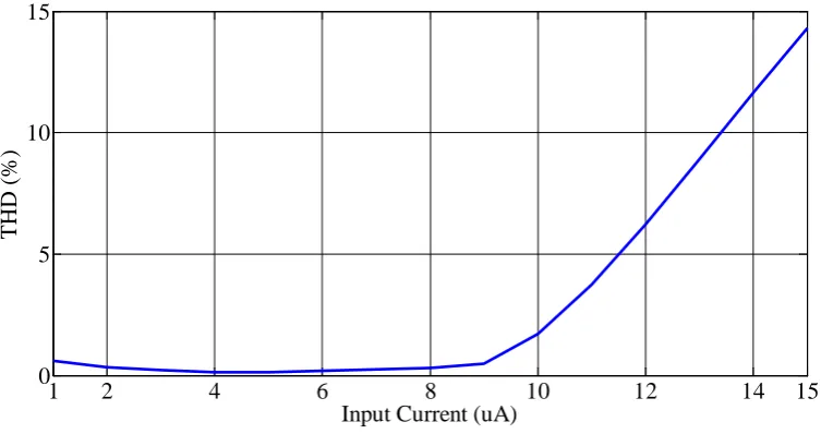
Figure 7.THD variations of the output waveform of band pass filter.
105 106 107 108
-80 -60 -40 -20 0
Frequency (Hz)
N
o
rm
al
ize
d
G
ai
n
(
d
B
)
HP Ideal BP Ideal LP Ideal HP Non-ideal BP Non-ideal LP Non-ideal
105 106 107 108
-35 -30 -25 -20 -15 -10 -5 0
Frequency (Hz)
N
o
rm
al
ize
d
G
a
in
(
d
B
)
1
2
4
6
8
10
12
14
15
0
5
10
15
Input Current (uA)
T
HD (
%
[image:6.595.126.503.505.704.2](a)
[image:7.595.74.539.79.457.2](b)
Figure 8. (a) Monte Carlo analysis of the proposed configuration for Q0 for 10% variations in R5; (b) The respective
histo-gram.
Figure 9. Input and output waveforms of the band-pass filter of the proposed circuit for 10 MHz sinusoidal input current of
10 uA.
high pass (all normalized responses) of circuit of Figure 3 are given in Figure 5. In Figure 5 we have shown two responses; one (by continuous line) while employing MOS CDBA ofFigure 4 and the other (by dashed line) while employing ideal CDBA of Figure 1(b) in the circuit configuration ofFigure 3. These responses are fairly
104 105 106 107 108
-30 -25 -20 -15 -10 -5 0
Frequency (Hz)
N
o
rm
al
ize
d
G
a
in
(
d
B
)
1 1.10 1.20 1.30 1.40 1.50
-1 -0.5 0 0.5 1
Time ( micro seconds)
N
o
rm
al
is
e
d
V
a
lu
e
[image:7.595.154.467.495.647.2]close and are in agreement with our proposed scheme. The difference in these continuous line and dashed line responses are mainly attributed to non-ideal port transfer ratios of the CDBAs used which is clear from the non-ideal expressions of ω0 and Q in Equation (8a) and (8b).
The simulation was performed for the proposed filter with the center frequency of 10 MHz and a quality fac-tor of Q = 0.707. To test the tunability of the circuit, the variation in the quality factor with resistance R5 was observed. The variation of the quality Q with R5 has been presented inFigure 6. The limited bandwidth and the non-idealities of the CDBA cause the filter response to deviate from the ideal response at high frequencies.
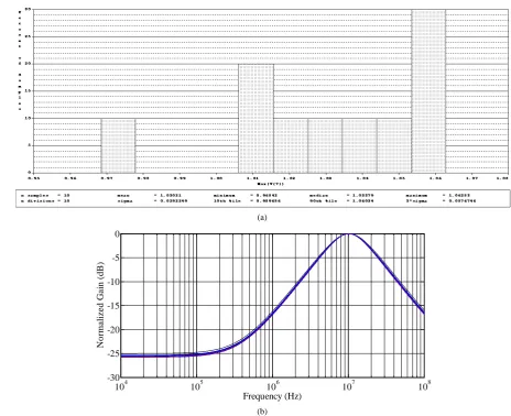
The Total Harmonic Distortion (THD) at output current on input current amplitude of the band-pass filter rea-lized from the proposed configuration is shown inFigure 7. We have carried out Monte Carlo analysis of the proposed configuration for its Q deviation for ±10% variations in R5 and the result is given inFigure 8(a) and Figure 8(b). The corresponding Q deviation shown in Figure 8 is not discouraging. The input dynamic range of the proposed filter configuration is shown at to 10 uA without any significant distortion as shown in Figure 9. Normalized values have been used here because of the nature of the filter i.e. TR mode.
7. Conclusion
This paper proposes a new CDBA based KHN-equivalent biquad circuit which employs three CDBAs, two grounded capacitors, one grounded resistor and four virtually grounded resistors. It has been implemented using PSPICE. The proposed circuit has the following advantages: a) all the capacitors are grounded and the resistors are directly or virtually grounded, which is important for its implementation as an integrated circuit. b) The cir-cuit is of Single-Input Multiple-Output (SIMO) type which can be used in a situation which requires the three filter functions (LP, HP and BP) simultaneously. c) Since the circuit is of trans-resistance type which acts as a current to voltage convertor, that interconnects voltage mode and current mode circuits. d) This circuit works at a considerable high frequency and also has an independent tunability of Q. e) the circuit has low passive and ac-tive sensitivity values. The simulated result agrees with the theoretical analysis to a high degree.
References
[1] Kerwin, W.J., Huelsman, L.P. and Newcomb, R.W. (1966) State-Variable Synthesis for Insensitive Integrated Circuit Transfer Functions. IEEE Journal of Solid-State Circuits, 2, 87-92. http://dx.doi.org/10.1109/JSSC.1967.1049798 [2] Senani, R. and Singh, V.K. (1995) KHN-Equivalent Biquad Using Current Conveyors. Electronics Letters, 31, 626-
628. http://dx.doi.org/10.1049/el:19950422
[3] Toker, A. and Acar, C. (1999) Current-Mode KHN-Equivalent Biquad Using CDBAs. Electronics Letters, 35, 1682- 1683. http://dx.doi.org/10.1049/el:19991179
[4] Acar, C. and Ozoguz, S. (1999) A New Versatile Building Block: Current Differencing Buffered Amplifier Suitable for Analog Signal-Processing Filters. Microelectronics Journal, 30, 157-160.
http://dx.doi.org/10.1016/S0026-2692(98)00102-5
[5] Özcan, S., Kuntman, H. and Uzhan Çiçekolu, O. (2002) Cascadable Current Mode Multipurpose Filters Employing Current Differencing Buffered Amplifier (CDBA). AEU-International Journal of Electronics and Communications, 56, 67-72. http://dx.doi.org/10.1078/1434-8411-54100075
[6] Pathak, J.K., Singh, A.K. and Senani, R. (2013) New Voltage Mode Universal Filters Using Only Two CDBAs. ISRN Electronics, 2013, Article ID: 987867. http://dx.doi.org/10.1155/2013/987867
[7] Keskin, A.Ü. and Hancioglu, E. (2005) Current Mode Multifunction Filter Using Two CDBAs. AEU-International Journal of Electronics and Communications, 59, 495-498. http://dx.doi.org/10.1016/j.aeue.2005.01.003
[8] Bashir, S.A. and Shah, N.A. (2012) Voltage Mode Universal Filter Using Current Differencing Buffered Amplifier as an Active Device. Circuits and Systems, 3, 278. http://dx.doi.org/10.4236/cs.2012.33038
[9] Özcan, S., Kuntman, H. and Uzhan Çiçekolu, O. (2002) Cascadable Current Mode Multipurpose Filters Employing Current Differencing Buffered Amplifier (CDBA). AEU-International Journal of Electronics and Communications, 56, 67-72. http://dx.doi.org/10.1078/1434-8411-54100075
[10] Sagbas, M. and Köksal, M. (2005) A New Multi-Mode Multifunction Filter Using CDBA. Proceedings of the 2005
European Conference onCircuit Theory and Design, 2, 225-228. http://dx.doi.org/10.1109/ECCTD.2005.1523034 [11] Tangsrirat, W., Klahan, K., Dumawipata, T. and Surakampontorn, W. (2006) Low-Voltage NMOS-Based Current