A CMOS Band Gap Reference Generator for
Low Voltage Amplification with the Application
of a (-ve) Feedback Loop
Niranjan Bhattacharyya
Research Scholar, Singhania U Rajasthan
Tanima Ghosh
Lecturer,BPIT Delhi-110089
ABSTRACT
We all know that the basic building block of any communication system is the reference voltage generator. The objective of reference generation is to establish a DC voltage or current that is independent of the supply and process and has a well-defined behavior with temperature. Band Gap Reference (BGR) is one of the most popular reference generators. In the conventional BGR circuit, the reference voltage Vref is the summation of thermal voltage VT and the base to emitter voltage of a transistor (Vf).The thermal voltage VT has a (+Ve) temperature coefficient (TC), whereas Vf has a (-Ve) temperature coefficient (TC).So BGR is independent of temperature .The traditional BGR circuit generates a reference voltage about 1.12V.So this circuit limits a low supply-voltage operation below 1v. In this paper a new BGR circuit in 0.25μm iCMOS technology, and a new BGR in BiCMOS technology is proposed which are containing a extra (-ve) feedback loop to get very low reference voltage as well as to stabilize this reference voltage even when it is operating below 1v supply. The TC of this reference generator is getting even zero by applying a (-ve) feedback loop. For a temperature variation between -400 C and 1000 C,the BGR of CMOS technology, and for a temperature variation between -400 C and 600 C, the BGR of BiCMOS technology, the produced reference voltages are absolutely independent of temperature variation together with the capability of operating at very low supply voltage (less than 1V).
1. INTRODUCTION
Reference voltage generators are used in A/D converters, D/A converters, DRAM’s, flash memories, and so many applications in communication field.
Reference voltages or currents that exhibit little dependence on temperature prove essential in all analog circuits. Temperarure dependence of the reference voltage is definitely one of the most important issue in BGR design, as it directly affects the performance of such circuits. The output voltage of the conventional BGR is 1.25V which limits the operation of the BGR below 1.2V supply. To overcome this problem we use the conception of [12] fig1 to get a CMOS BGR operating below 1V supply .But we modify the OPAMP /Differential Pair by using a current mirror active load to get a better result[6]. The BGR obtained by the combination of
these two idea we make a hybrid BGR circuit as shown in fig2.But this Hybrid BGR is also not absolutely temperature independent. To make it absolutely temperature independent we use a (-ve) feedback loop, that feeds a little part of the output voltage to the input in out of phase. We also use the conception of Voltage Divider biasing conception to make the proposed BGR more stable.
We know that BiCMOS technology is one of the leading technologies now a day. So use the same conception of (-ve) feedback to make the existing BiCMOS BGR of Marcovati[8]more stable. Before come to the circuit description and theory we want to go through some important points described below.
2. CIRCUIT DESCRIPTION AND
OPERATION AND RESULT OF
PROPOSED BGR IN CMOS
TECHNOLOGY
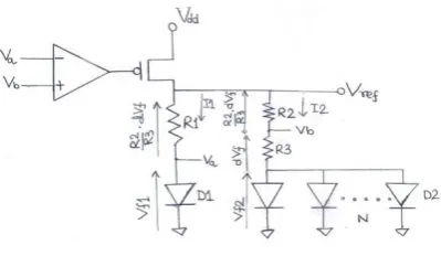
[image:1.595.320.520.515.631.2]The conventional BGR circuit is composed of a CMOS op-amp, diodes and resistors. This circuit is shown in below:
Fig 1.Conventional BGR Circuit
)
1
(
KTqV
S f
e
I
I
≈ KT
qV
S f
e
I
[As
V
f is much greater thanq
KT
]
Is
I
V
V
f
T
ln
Where K is the Boltzmann’s constant (1.38*10-23 J/K) and q is the electronic charge (1.6*10-19C).
In the conventional circuit, a pair of input voltages for the op-amp Va and Vb, are controlled to be the same voltage. dVf is the forward voltage difference between one diodeD1 and N diodes d2.
2
1 f
f
f
V
V
dV
=
)
ln(
1 2
R
R
N
V
T
……… …….. (3)
The BGR output voltage
V
ref then becomescon ref f
ref
df
V
R
R
V
V
3 2 1
1
f
V
has a negative temperature coefficient ofc
mv
/
02
whereasV
T has a positive temperature coefficient of0
.
086
mv
/
0c
.
Thus the
V
ref is determined by the resistance ratio. Thevalue of
V
ref is about 1.25V which limits thelow-voltage design for the CMOS circuit.
The concept of the proposed BGR is that two voltages
T
V
andV
fare generated by only one feedback loop. The PMOS transistor dimensions of p1, p2 and p3 are the same, and the resistance values of R1 and R2 are same.We know that if the gates of PMOS transistors are connected they will draw equal currents. For the same
reason,
I
1
I
2
I
3.
In this case,
I
1a
I
2aandI
1b
I
2b.)
ln(
2
1
V
V
N
V
dV
f
f
f
T
a
I
2 is proportional toV
T3 2
R
dV
I
a
fb
I
2 is proportional toV
f12 1 2
R
V
I
b
fHere,
I
2 is the sum ofI
2a andI
2b, andI
2 is same asI
3,3 2 2a 2b
I
I
I
I
Therefore, the output voltage of the proposed BGR,
V
ref ,becomes
1 4
2 3
(
f f)
ref ref prop
V
dV
V
R
V
R
R
If the resistor and diode parameters for the proposed BGR are
the same as those for the conventional BGR,
V
refpropissimplified as 4 2
ref prop ref con
R
V
V
R
Therefore,
V
refpropcan be freely changed fromV
refconof1.25V.
V
ref For the proposed BGR is determined by theresistance ratio of R2, R3 and R4 and little influenced by the absolute value of the resistance. The transistors M1, M2 and M3 must operate in the saturation region, so that their drain-to-source currents are reduced.
We also modify the OPAMP to operate at low power supply voltage(1v)[6]
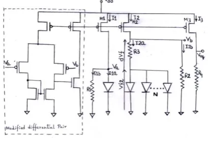
[image:2.595.326.531.441.581.2]Implementation an OPAMP with 1V power supply is challenging. The OPAMP is modified as shown in fig.2.
Fig.2 Hybrid BGR
Using this modified OPAMP and the theory explained above the BGR circuit generated is named as Hybrid BGR is shown in Fig2. This Hybrid BGR can operate definitely in sub 1V supply and can generate a reference voltage much lower than 1V, but the TC of the BGR output voltage is not zero. The BGR voltage varies with temperature ,though this variation is very low.
We all are familiar with the (-ve) feedback amplifier. In (-ve) feedback technique a very little part of output voltage or current are feeding to the input of the amplifier in out of phase. As a result the variation of the output voltage with the variation of the temperature reduces. And as a result we used to get a stable output even at the variation of the temperature in a large scale. This conception is used in this Proposed BGR circuit as well.
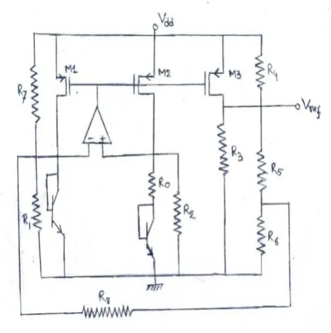
[image:3.595.324.532.75.294.2]In the Hybrid BGR, we get a low voltage at the output of BGR, but this voltage varies with temperature. When we add the feedback loop at the output of the same BGR we get a fully constant output with respect to the variation of temperature. The new Proposed BGR with feedback loop is shown in fig.3.
Fig.3 Modified Hybrid BGR
The output of the proposed BGR is lower than the Hybrid BGR at the same supply voltage for every equal conditions. So we can say that the feed back is a voltage series feedback
We also used the voltage divider biasing circuit to stabilize the operating point of the proposed BGR.
We also used the conception of voltage divider biasing to stabilize the proposed BGR circuit. In proposed BGR there is no change of BGR voltage when the temperature is changing from -40 degree centigrade to 100 degree centigrade. The BGR voltage is absolutely constant with Zero( 0 ) TC.
3. OBSERVATIONS AND RESULT
In proposed BGR we not only get a absolutely stable voltage , the range of operation also becomes wider The comparison between the Hybrid BGR and the proposed BGR is shown in tabular form in Table1
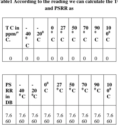
Table1 According to the reading we can calculate the TC and PSRR as
TC in ppm/o C.
-40 0
C
-200 C
0 0
C 27 0
C 50 0
C 70 0
C 90 0
C 10 00 C
0 0 0 0 0 0 0 0 0
PS RR in DB
-40 0
C
-20 0
C 00 C
27 0
C 50 0
C 70 0
C 90 0
C 10 00 C
7.6 60
7.6 60
7.6 60
7.6 60
7.6 60
7.6 60
7.6 60
7.6 60
7.6 60
From the comparison Table1 it is clear that the proposed BGR is much more better than the Hybrid BGR is all aspects.
4. PROPOSED BICMOS BGR
What is BiCMOS technology?
When both npn and pnp bipolar transistors can be added to a CMOS process, which is then called a BiCMOS process. These processes tend to be used for specialized analog or high-voltage circuits. In a regular n-well process, a parasitic pnp transistor is present that can be used for circuits such as Band gap voltage references. This transistor is shown in Fig4 with the substrate collector, the n-well base, and the p-diffusion emitter.
CIRCUIT AND THEORY:
Two components build up the output voltage of a band gap reference one is the voltage across a directly biased diode and other is a term proportional to the absolute temperature. The (-ve) temperature coefficient of the former tern compensates the
(+ve) temperature coefficient of the latter. If
V
T
kT q
/
is used to obtain a PTAT voltage we have to multiply VT by approximately 25 to compensate for the temperature dependence of the diode voltage. If this condition is satisfied, the generated band gap voltage becomes approximately 1.2v.Using a supply voltage (VDD) as low as 1v,obviously 1.2v cant be produced, we can generate a fraction of 1.2v with similar temperature features. Since the Band Gap voltage is given byBG BE
kT
V
V
n
q
………..(1)The temperature dependence of the resistors used is compensated by fabricating them always with the same kind of material. Fig 1shows the block diagram of the BGR in BiCMOS technology by Malcovati. diode connected bipolar transistors drain the same current given the used emitter area ratio, N, ∆VBE is equal to
V
Tln( )
N
.Therefore, the currentin R0 is PTAT.The operational amplifier forces the two voltages VA and VB to be equal, thus producing a current in the equal resistors R1 and R2 proportional to VBE. As a result the current in M1,M2 and M3 (I1=I2=I3) is given by
1
0 1
ln( )
T BE
V
N
V
I
R
R
……….(2)The output voltage is given by
…… 3 3
1 3
0 1
ln( )
(
)
(
)
out T BE
R
n
R
V
I R
V
V
R
R
…….(3)The temperature coefficient of resistor is cancelled if resistors are made withtthe same resistive layer. The compensation of the temperature coeffof VT and VBE is ensured by a proper choice of N and of the
R
0/
R
1 ratio By I Inspection of thecircuit we observe that the minimum supply voltage is determined by the VBE plus a saturation voltarange of a p-channel transistor. Therefore, 1v can be enough to opera initiate the circuit.
OPERATIONAL AMPLIFIER DESIGN
Theband gap circuit needs an operational amplifier whose input common mode voltage is around 0.65v (the VBE ).also since the output nodedrives p-channel current sources, its
quiescent voltage should be belo
V
DD
Vth p
, .
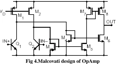
Assuming VDD=1v and Vth,p =0.7v the output volt resulis as low as 0.15-0.2v.Moreover, the gain of the Opamp must be arou 60dB without any bandwidth constraints. The above design cond itionstion lead to the following considerations[8] [image:4.595.57.267.493.605.2]Malcovati designs the OPAMP for low voltage operation amplifier is shown below in Fig4
Fig 4.Malcovati design of OpAmp
The considerations for design of OPAMP in BiCMOS technology for low voltage power supply are:
1. The input common mode voltage makes it difficult to accommodate an n-channel input differential stage. Possible, a level shift of the input voltages by 150-200 mv is necessary.
2. The low output voltage prevents the use of cascode configurations. Therefore, two-stage architectures should be used.
3. The required biasing conditions can lead to a significant offset, which can become the key limit to the correct operation of the Band Gap circuit.
A careful analysis of the above issues shows that we can use a CMOS technology with a supply only if the thresholds of the n-channel and p-channel devices are 0.5v or below. However, a BiCMOS technology (or a CMOS with lateral BJT) allows us to design an Operational amplifier suitable for 1v operation even with threshold voltages 0.7v.So according to Malcovati,and after the modification of the OPAMP the BGR circuit achieves 5ppm/k degree of accuracy.
The new OPAMP circuit does not use an differential stage but two grounded bipolar transistors.
The combination of the diode connected BJT in the band gap and the BJT of the input stage constitutes a current mirror. Therefore, the currents in the input stage of the operational amplifier do not need control, being a replica of the current in the band gap structure. Two diode connected MOS devices receive the signal current and lead to the following differential gain
,
, ,
/
2
/ (
)
m BJT BJT T
d
m MOS MOS GS Th n
g
I
V
A
g
I
V
V
….(4)Where the suffix BJT refers to the input BJT and the suffix MOS refers to the diode loads M3 and M4.Assuming (VGS – VTH,n) = 4VT and using IBJT =4IMOS with a gain of 16. Since the input gain stage is fully symmetrical its systematic offset is zero. Moreover, a possible offset from the second stage is divided by 16.The second stage is a push-pull circuit. Since the quiescent value of the output voltage is one VGS,p below VDD , the VDS voltages of M7 and M8 match and the systematic offset of the second stage is zero as well. The bias current used is kept at a very low level,since we want to maximize the gain and bandwidth is not important. However, since the bias current of the circuit has a PTAT feature power consumption will increase proportionally to the absolute temperature. This variation is irrelevant even when using the circuit in the range from -200c to 1200c.The operational amplifier was designed using a 0.8um BiMOS technology.
Fig.5 Optimum BGR
5.
RESULT
According to the reading we can calculate the TC and PSRR as
TC in - - 0 27 50 70 90 10
ppm/0 C.
40 0
C
200 C
0
C 0
C 0
C 0
C 0
C 00 C
0 0 0 0 0 0 0 0 0
PSRR in DB
-400 C
-200C
00 C 270 C 500 C 700 C 900 C 1000
C
.1716 .1716 .1716 .1716 .1716 .1716 .1716 .1716 .1716
It is clear from the above table that the output of the BGR is absolutely constant for the temperature range shown above. But the drawback of the circuit is that it can not give a constant output beyond this temperature range. Also the PSRR of both the circuits are very low.
6. CONCLUSSION
The proposed BGR in CMOS and Bi-CMOS technology can give a constant output voltage with the variation of temperature from -400c to 1000c with the supply voltage variation as lower as possible to as higher as possible .we can say that it is a versatile achievement. But the drawback of these circuits are that ,their stability is very much dependent on the resistance values and their PSRR are very low. So in future we will try to get BGRs having higher PSRR and lesser dependency on resistance values.
7. REFERENCES
[1] Novel CMOS gap Ref circuit with Improved High-Order Temperature Compensation by Koudounus etc.,University of Cyprus,A IEEE Journal of 2010.
[2] “A high precision high PSRR band gap reference with thermal hysteresis protection by Yang Yitang etc, A journal of Chinese Institute of Electronics, Sept 2010
[3] Design of Band Gap Reference and Current reference Generator with Low supply voltage by Dong-OK Han etc., IEEE journal of 2008.
[4] ‘Low-Voltage Band Gap Reference Design Utilizing Schottky Diodes’ by David L. Butler and R. Jacob Baker. An IEEE journal of 2005.
[5] ‘Novel Start-Up Circuit With Enhanced Power-Up Characteristic For Band Gap references’ by Tuan Vu Cao, etc
An IEEE journal of 2008
[6] ‘A Sub-1-V Linear CMOS band Gap Voltage Reference’ by Yang Welli,Wang Xichuan, Caj Jun’ A journal of Microelectronic Research & Dev Centre,Shanghai U.