http://dx.doi.org/10.4236/epe.2015.75020
Influence of a Semiconductor Gap’s
Energy on the Electrical Parameters
of a Parallel Vertical Junction
Photocell
Nfally Dieme
Laboratory of Semiconductors and Solar Energy, Department of Physics, Faculty of Science and Technology, Cheikh Anta Diop University, Dakar, Senegal
Email: [email protected], [email protected]
Received 15 March 2015; accepted 12 May 2015; published 14 May 2015
Copyright © 2015 by author and Scientific Research Publishing Inc.
This work is licensed under the Creative Commons Attribution International License (CC BY).
http://creativecommons.org/licenses/by/4.0/
Abstract
The present work is a theoretical study on a parallel vertical junction solar cell under a multi- spectral illumination in static regime. The density of the minority charge carriers was determined based on the diffusion equation. Photocurrent and photovoltage are deducted from such density. All these parameters are studied taking into account the influence of the gap energy (Eg).
Keywords
Vertical Junction, Energy Gap, Photocurrent Density, Photovoltage
1. Introduction
The operation of solar cells is basically dependent on photon-electron interaction. For an electron to be removed from the valence stripe to the conduction, the minimum value of the photon energy must at least equal Eg. The gap energy (Eg) is determined by the material and fluctuates according to temperature [1].
The aim of this work is to investigate the influence of gap energy (Eg) on electrical parameters such as photo-current and photovoltage. Knowing the evolution of these two quantities based on the gap energy is a good in-dicator for us to comment on the performance of solar cells and types of semiconductors for use in the manufacture of solar cells able to run at high temperature.
2. Theory
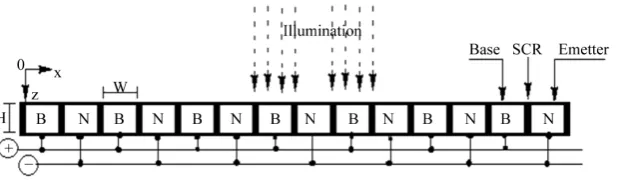
This study is based on a parallel vertical junction silicon solar cell [2] presented inFigure 1. The solar cell is il-luminated along the z axis in steady state.
We assume that the following hypotheses are satisfied. • The contribution of the emitter is neglected.
• Illumination is made with polychromatic light, and is considered to be uniform on the z = 0 plane. • There is no electric field without space charge regions.
2.1. Density of Minority Charge Carriers
When the solar cell is illuminated, there are simultaneously three major phenomena that happen: generation, diffusion and recombination.
These phenomena are described by the diffusion-recombination equation obtained with:
( )
( )
( )
2
2 2
n x n x G z
D
x L
∂
− = −
∂ (1)
D is the diffusion constant and is related to the operating temperature through the relation [2]
K
D T
q
µ
= ⋅ ⋅ (2)
with q as the elementary charge, k the Boltzmann constant and T temperature.
G(z) is the carrier generation rate at the depth z in the base and can be written as [2] [3]:
( )
e b zi iG z =
∑
a − (3)ai and bi are obtained from the tabulated values of AM1.5 solar illumination spectrum and the dependence of the absorption coefficient of silicon with illumination wavelength.
n(x), L, τ, and μ are respectively the density of the excess minority carriers, the diffusion length, lifetime and mobility.
The solution to the Equation (1) is:
( )
sinh x cosh x ai 2eb zin x A B L
L L D
−
= + +
∑
(4)Coefficients A and B are determined through the following boundary conditions: at the junction (x = 0):
( )
( )
0 0 f x S n x nx = D
∂
=
∂ (5)
This boundary condition introduces a parameter Sf which is called recombination velocity at the junction; Sf determines the flow of the charge carriers through the junction and is directly related to the operating point of the solar cell. The higher Sf is, the higher the current density will be.
[image:2.595.160.470.614.705.2]In the middle of the base (x = W/2):
( )
2 0 w x n x x = ∂ =∂ (6)
Equation (8) illustrates the fact that excess carrier concentration reaches its maximum value in the middle of the base due to the presence of junction on both sides of the base along x axis (Figure 1).
2.2. Photocurrent Density
The photocurrent Jph is obtained from the following relation given that there is no drift current:
( )
0 ph x n x J qD x = ∂ =∂ (7)
2.3. Photo-Voltage
The photo-voltage derives from the Boltzmann relation:
( )
2 0 ln 1 ph B i n k T V N q n ⋅ = ⋅ ⋅ + (8) with 3 2 exp 2 g i n E n A T
KT
= ⋅ ⋅
(9)
nirefers to the intrinsic concentration of minority carriers in the base, Anis a specific constant of the material (An =3.87 10× 16 for silicon)
NBis the base doping concentration in impurity atoms Eg is the energy gap; it is given by [4] [5]:
0 2 g g a T E E b T ⋅ = −
+ (10) (
0 1.170 eV
g
E = ; 4 2
4.9 10 eV K
a= × − ⋅ − ; b=655 K for silicon).
3. Results and Discussion
In this section of our work, we present the results obtained from simulations.
3.1. Gaps Energy
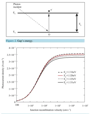
When the solid temperature tends to absolute zero, two allowed energy bands play a special role. The last com-pletely filled band is called “valence band: EV”. The allowed energy band is called following the “conduction band:
EC”. It can be empty or partially filled. The energy between the valence band to the conduction band is called the
“energy gap: Eg” [6].Figure 2 illustrates the band representation.
To have extraction of electrons under the influence of light, incident photon must have an energy greater than or equal to the energy of the gap. Eg =EC−EV. The gap energy is the energy that electron must absorb to be ex-
tracted.
3.2. Photocurrent Density
Figure 3 shows the photocurrent density profile versus junction recombination velocity for various values of energy gap.
Figure 2. Gap’s energy.
Figure 3. Photocurrent density versus junction recombination velocity (z =
10−2 cm).
It can also be seen that the increase in the material’s gap energy causes a decrease in the photo-courant densi-ty. This variation is much more visible in short circuit situations.
Indeed, photocurrent is produced by a movement of carriers photo-generated through the junction. When the height of the barred band increases, many electrons are extracted with low kinetic energy [7] [8]: this phenol- menon is called the photoelectric effect:
cinetik photon g.
E =E −E
Consequently the diffusion of carriers through the junction weakens as some carriers do not have enough ki-netic energy to jump the depletion zone. It is said that photocurrent density decreases as the gag energy (Eg) in-creases.
3.3. Photo-Voltage
Figure 4shows the evolution of photo-tension depending on recombination velocity at the junction regarding different values of the material’s gap energy Eg.
Figure 4 shows that photovoltage decreases along with Sf junction recombination velocity. When Sf increases, the flow of charge carriers crossing the junction increases. Thus, fewer and fewer carriers are stored, which causes decrease in photovoltage at the junction.
and start piling up, thus increasing the difference in potential at the junction: it is said that photovoltage in- creases when Eg is high.
[image:5.595.177.449.290.513.2]3.4. Current-Voltage Characteristics
Figure 5 shows the evolution of photo-courant density for different values of the gap energy and in relation to photo-tension.
Figure 4 shows that when photo-courant is maximized, photo-tension nears the zero level and vice versa. It can be noted that this figure perfectly confirms variation of the two physical quantities (photovoltage and photocurrent) in relation to gap energy. It can also be seen that when there is an increase in Eg of
3
4 10 eV g
E −
∆ = × ,
photo-voltage increases by almost 10% while photocurrent decreases by about 2%.
4. Conclusion
In the simulation carried out in this work, we have demonstrated that the electric quantities of a solar cell such as photovoltage and photocurrent are very sensitive to the variation of a material’s gap energy. Under the influence of temperature, an increase in the gap energy of ∆Eg = ×4 10−3eV can prompt a growth in photovoltage of
[image:5.595.156.471.541.708.2]Figure 4. Photo-voltage versus junction recombination velocity (z = 10−2 cm).
almost 10% and a decrease in photocurrent of about 2%. We can estimate that according to experience, semi- conductors have a great height of the band gap such as GaP, GaN, which are most suitable for high operating temperatures. This theoretical study can be confirmed by a comparative study of the conversion efficiency of semiconductor of different energy gap.
References
[1] Levy, F. (1995) Traité des matériaux 18: Physique et technologie des semi-conducteurs, Presses Polytechniques et Universitaires Romandes.
[2] Dieme, Nf., Zoungrana, M., Mbodji, S., Diallo, H.L., Ndiaye, M., Barro, F.I. and Sissoko, G. (2014) Influence of Temperature on the Electrical Parameters of a Vertical Parallel Junction Silicon Solar Cell under Polychromatic Illu-mination in Steady State. Research Journal of Applied Sciences, Engineering and Technology, 7, 2559-2562.
[3] Furlan, J. and Amon, S. (1985) Approximation of the Carrier Generation Rate in Illuminated Silicon. Solid-State Elec- tronics, 1241-1243.http://dx.doi.org/10.1016/0038-1101(85)90048-6
[4] Sze, S.M. and Kwok, K.Ng. (2007) Physics of Semiconductor Devices. Third Edition, John Wiley & Sons, Hoboken. [5] Pässler, R. (2003) Semi-Empirical Descriptions of Temperature Dependences of Band Gaps in Semiconductors. Phy-
sica Status Solidi,710-728.
[6] Valkov, S. (1994) Electronique Analogique. Edition Castéilla, Collection A. CAPLIEZ.
[7] Agroui, K. (1999) Etude du Comportement Thermique de Modules Photovoltaïquesde Technologie Monoverre et Biverre au Silicium Cristallin. Revue des Energies Renouvelables: Valorisation, 7-11.
[8] Mohammad, S.N. (1987) An Alternative Method for the Performance Analysis of Silicon Solar Cells. Journal of Ap-plied Physics, 767-772.http://dx.doi.org/10.1063/1.338230