© 2017, IRJET | Impact Factor value: 5.181 | ISO 9001:2008 Certified Journal
| Page 23
An Efficient Real-Time Controller for Retrieving Multimedia Data from
Secured Digital High Capacity Card
Sekata Olika Abdenaa
1, Dr. Vasu Pinnti
21
Dean, College of Engineering, Wolaita Sodo University, Sodo, Ethiopia
2
Associate Professor, ECE Dept, College of Engineering, Wolaita Sodo University, Sodo, Ethiopia
---***---Abstract -
Real-time multimedia data access plays an
important role in electronic systems; as time goes by,
with decrease in data processing speed and increase in
communication time, storage time, access time, and the
overall response time increases for real-time
applications. Therefore, in our paper, a fast and efficient
real-time controller has been proposed and implemented
where large volume of multimedia data can be efficiently
and effectively stored and retrieved from flash memory
cards. It is being implemented only using hardware
description language (HDL) on a field programmable
gate array (FPGA) chip without using any other external
hardware resources or high-level languages. The entire
controller architecture, in a single chip, contains 5
variant modules and is designed and developed using
finite state machine (FSM)-based approach. The modules
are Card Initialization Module (CIM), Idle Module (IM),
card Access module (CAM), card store module (CSM), and
decision making module (DMM). The experimental
results tested for microSD, and SDHC cards of different
size, and these show that the architecture uses less
hardware and clock cycles for card initialization and
single/multiblock read/write procedure.
Key Words
:
multimedia, Real-time controller, card
initialization, decision making,
1. INTRODUCTION
The flash-based storage device, introduced by Toshiba in 1984, is basically a non-volatile memory and used whenever a shock resistance is the key requirement of any application [1]. The Secured Digital High Capacity (SDHC) card is mainly designed to meet certain requirements such as security, capacity, performance, and environmental issues inherent in newly emerging audio and video consumer electronic devices. The SD (Secured Digital) card standard is designed and Developed by SD Card Association [2] and is a collaborative effort of the three (3) manufacturers, namely Toshiba, SanDisk, and MEI [3].
The SD card includes an on card intelligent controller to handle the security algorithms, interface protocol, data storage and retrieval, error handling and corresponding
error correction code (ECC) algorithms, defect handling diagnostics, power management, and clock control [1]. However, to interface the SDHC card (slave unit) with master unit (e.g., computer, any application-specific device or host), we need a system which can communicate with the on-card controller of the SDHC card for smooth execution of single/multi block data read/write.
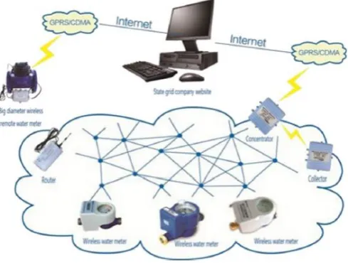
Fig.1 represents a model of a data archival system and it shows that how the flash - based memory cards like micro SD or SDHC cards can be used as the plug and play memory module for real-time application. Generally, the signal is received from the external world in a buffer, converted into a serial bit stream and subsequently stored into the memory card. The stored data at later stage may be transmitted for further processing. Also, the flash memory acts as a small, portable unit and it can be removed from the system where it is presently housed in and accessed by some other system to retrieve the desired signal.
Fig. 1 A model of a data archival system
[image:1.595.308.571.454.556.2]© 2017, IRJET | Impact Factor value: 5.181 | ISO 9001:2008 Certified Journal
| Page 24
Fig. 2 Block diagram of a real-time data concentratorsystem
In these application scenarios, the efficiency of single and multi-block data transfer is very important which consequently affects the input and output operations per seconds (IOPS) measure of storage system. Generally, we wish to maximize this metric with respect to different types of flash as this indicates the measure of flash utilization. As stated that, flash-based memory system can be used as a cache or a data concentrator or to cater any such storage requirements. However, here in this paper, we do not analyze the pros and cons of such utilization of flash in detail. The work mainly concentrates on efficient implementation of a real-time controller for single or multi-block data transfer with respect to flash memory. The implementation may be exploited in any kind of flash memory resource utilization and ultimately contribute in the calculation of the metric of memory resource utilization. Therefore, it is clearly observed that the implementation of an efficient and effective flash-based data transfer is a fundamental driving factor in the improvement of flash resource utilization and this paper is focusing on that rudimentary aspect.
The flash based memory cards like micro SD or SDHC cards work in two different bus modes. They are the Secure Digital bus mode (SD BUSMODE) and the Serial Peripheral Interface bus mode (SPIBUS MODE). The SPI bus mode is a synchronous serial protocol with very less complexity. It is extremely very popular for interfacing the peripheral devices and no native host interface is needed for this bus mode. For its simplicity and usefulness in the low cost embedded system application, we have considered designing an entirely on-board hardware-based controller for smooth realization of SPI bus mode -based data transfer protocol to communicate with the flash-based memory card.
Until to date, we find that very limited research work describes the design of data archival system and the
subsequent implementation using HDL [1]. In some research work, SPI bus mode-based data communication system has been implemented. Another work was proposed in the literature where the SDHC card had been used in SD mode (i.e., bulk data transfer mode) for video signal storage and processing [14]. With the newly emerging technologies, flash-based memory devices have been used as the most efficient storage unit and till now it accomplishes the need of storage even on the modern era of technological advancement [2, 3, and 15].
Our paper proposes a real-time, low-cost, efficient application specific controller for multimedia data storage and retrieval for the flash based memory cards. The architecture of the real-time controller has been designed by using FSM-based approach. The HDL used for our work is Very high speed integrated circuit Hardware Description Language (VHDL). Also, the design is such that there is no use of any on-chip general purpose processor (GPP), external controller, hardware resources, or any high-level languages during the operation. The prototype has been entirely implemented in target FPGA board. The physical attribute of an FPGA chip, being compact in size and low in power consumption, makes it an ideal platform for the implementation. Also, we have tried to exploit the parallel processing capability of FPGA during design and implementation of various modules in this paper. The optimal in hardware implementation of such an application-specific controller and the study of its various modules were not explored in detail by earlier research. In this paper, the proposed controller has been examined for both the audio and video data storage and retrieval separately. Also we tried to establish the importance of the controller with respect to the flash read-write procedure.
Again in nutshell, the objectives of this paper are as follows:
1. To design a modular low-cost, system-on-chip, application-specific controller for the multimedia data storage and retrieval from the flash memory cards like SDHC, and micro SD card in SPI buss mode with less overhead.
2. The design is FSM based and the real-time controller has been primarily realized using five(5) different modules and a control unit. These five different modules, along with the control unit, are the different functional areas of the proposed system, which is implemented completely in a single chip.
© 2017, IRJET | Impact Factor value: 5.181 | ISO 9001:2008 Certified Journal
| Page 25
4. The controller will work in real time, in modular fashion and the implementation is on a single FPGA. The proposed design tries to utilize the parallel processing capability of FPGA. No other external devices or on-card intelligent controller has been used for this implementation.
2. REVIEW OF THE RELATED WORKS
FPGAs have been used for prototype design in a range of engineering application [1, 14–19]; however, till date to the authors’ knowledge, the design of a complete application-specific controller for different flash memory card access with detailed description of the modules and their operation is limited. Table 1 shows some of the earlier work in this domain.
Elkeelany et al. [1] proposed an FPGA based data archival system to Secure Digital card, using VHDL and they accessed the card in SPI bus mode. Scalability issues have not been achieved in this design. They have partially applied the FSM based approach and the implementation issues of all different SD cards have not been discussed explicitly in this paper.
Yang et al. [14] presented SD High Capacity card video player based on SOPC technology. The IP core and display buffer SRAMs were alternately utilized for their proposed design. They have accessed SDHC card in SD bus mode for bulk data transfer. The proposed design has been implemented using high-level language.
In another work, Abdallah and Elkeelany [15] proposed a FPGA based simultaneous multi-channel data acquisition system and they had verified the proposed architecture for the analog signals. The design includes analog-to-digital converter to convert the analog signal to digital data. The time-critical tasks were implemented in hardware, while the other tasks were implemented using embedded C. The use of the high-level language in this paper makes the system slower with additional overhead.
Lin and Dung [16] proposed a NAND flash memory controller for sd Multimedia Card (MMC). They had designed Bose-Chaudhuri-Hocquenghan (BCH) error correction code (ECC) [28] for correcting random bit errors of the flash memory chip. The UMC 0.18 μm CMOS process used to implement the memory controller chip. This controller was verified for MMC only.
The work, summarized in Table 1, has established the concept of FPGA-based implementation for the SD card data archival system either in SD mode or SPI mode. In this paper, we aim to design an application specific controller for efficient multimedia data communication with flash-based
cards in SPI mode and the controller architecture was entirely designed using FSM based approach.
Table -1: Existing papers on SD card controller design
Work Controller design
[1] Data archival to SD card using HDL
[14] Design of SDHC card video player on SoPC
[15] Simultaneous multi-channel data acquisition system
[16] NAND flash memory controller for SD/MMC card
[Proposed] FSM-based application-specific controller using HDL
There are mainly five states present in the proposed FSM and the states are named as initialization state, idle state, card-read state, card-write state, and decision-making state. During the realization of the controller architecture, these states are mapped into the modules of the controller. Now some of these modules are used to accomplish card read/write procedures and therefore internal architecture of those modules are again implemented based on FSM format for the realization of above procedures. Note that the proposed architecture and implementation aims to minimize both the clock utilization and on-board resource utilization of the FPGA board.
3. PROPOSED FPGA-BASED CONTROLLER
This section, first we are discussing the basic characteristics of the SD/SDHC card and micro SD card and second we are going introduce the proposed controller in rest of the section.
3.1 High capacity SD card
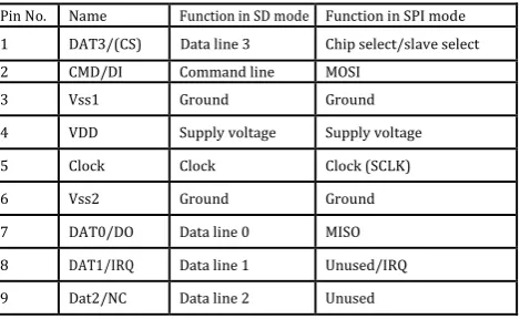
The SD/SDHC card communication is based on the advanced nine pin interface, that consists of a Clock, Command line/ Master Out Slave in (MOSI), 4 Data lines/ Master In Slave Out (MISO), and 3 Power lines. The card supports three communication protocols [21]. They are SD- 1 bit mode, SD- 4 bit mode, and SPI (Serial Peripheral Interface) bus mode. Table 2 depicts the pin configuration of the SD/SDHC card.
© 2017, IRJET | Impact Factor value: 5.181 | ISO 9001:2008 Certified Journal
| Page 26
[image:4.595.312.545.100.245.2]as (CMD55 + ACMD41) to complete the initialization process. The controller continuously generates (CMD55 + ACMD41) command until the card initiates itself by giving a ‘0000000’ response. The SDHC card supports two different kinds of addressing modes. One is block addressing mode and other one is byte addressing mode. The CMD58 command identifies the addressing mode of the version-2 SDHC card. Also, CMD 16 command is generated to fix the data block length to 512 bytes. After initialization process, the card goes to the idle state until the next command is being issued for single/multi block read/write.
Table 2 SD/SD High Capacity card pin details
Pin No. Name Function in SD mode Function in SPI mode 1 DAT3/(CS) Data line 3 Chip select/slave select
2 CMD/DI Command line MOSI
3 Vss1 Ground Ground
4 VDD Supply voltage Supply voltage
5 Clock Clock Clock (SCLK)
6 Vss2 Ground Ground
7 DAT0/DO Data line 0 MISO
8 DAT1/IRQ Data line 1 Unused/IRQ
9 Dat2/NC Data line 2 Unused
Throughout in our work, we used SDHC and SD card with speed classes 4 and 2, which means that the SDHC and SD card, used in this purpose, supports minimum 4 and 2 MB/sec writing speed, respectively, for video recording.
3.2 Micro SD card
[image:4.595.36.271.270.414.2]The micro Secure Digital card communication is much similar to the SD card communication. The difference between these two in the present age data storage medium is in their pin configuration. The micro SD communication is based on the 8-pin interface where all the pins from the SD card are present except the second ground (Vss2) pin.
Table 3 Micro Secure Digital card pin details
Pin No. Name Function in SD mode Function in SPI mode
1 Dat2/NC Data line 2 Unused
2 DAT3/( ¯ CS) Data line 3 Chip select/slave select (SS)
3 CMD/DI Command line MOSI
4 VDD Supply voltage Supply voltage
5 Clock Clock Clock (SCLK)
6 GND Ground Ground
7 DAT0/DO Data line 0 MISO
8 DAT1/IRQ Data line 1 Unused/IRQ
Table 3 shows the pin details of the micro SD card, and Fig. 3 illustrates the interfacing of the micro SD card with the Spartan3E target FPGA board.
Fig. 3 Micro Secure Digital (SD) card electrical interface with FPGA board
The micro SD card communication is also based on command dependent protocol, and it is almost similar to the SD and SD High Capacity card communication methods. The capacity of the micro SD card denotes how it works. If the capacity is less than or equal to 2 GB (≤ 2 GB), then the card works similar to the SD card; otherwise, the principle of operation is the same as the SDHC card.
The definition of the speed class for micro SD card is the same as the SD card [36]. We have used the class 4 micro SD card throughout the work, which means, the card supports 4 MB/s writing speed for video recording in a normal mode.
3.3 Architecture of the proposed controller
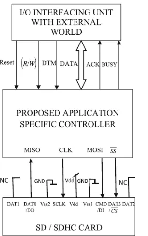
The workflow of the proposed host controller is based on the initialization of the card followed by data transfer (read/write) sequences. The overall external view of the controller interfacing the SDHC/SD card is given in Fig. 4. The same process can be used for interfacing the micro SD card also. The Vss2 pin remains unconnected when the process is used for interfacing the micro SD card as the card contains only 8-pin interface, and the Vss2 pin is not present in the physical architecture of the micro SD card.
The state diagram of overall control flow of the controller is shown in Figure. 5. The state diagram of Fig. 5 is working as a backbone for the architecture of the controller. The complete architecture has been implemented using VHDL. We observe from the above mentioned flow sequence and the schematic of the internal architecture, the pro-posed controller is divided into five variant modules. They are card initialization module (CIM), idle module (IM), card Access module (CAM), card storage module (CSM), and decision making module (DMM).
[image:4.595.35.273.614.730.2]© 2017, IRJET | Impact Factor value: 5.181 | ISO 9001:2008 Certified Journal
| Page 27
Fig. 4 Overall schematic of the proposed controllerEach of the modules and CU contains many internal and external data and control lines. The communication with the external world is done by the controller either using I/O interfacing units or a customized multiplexer.
The Reset, DTM (Data Transfer Mode), R/W , DATA, ACK, and BUSY signals are interfaced with the controller via I/O interfacing unit. The Reset signal, connected with CU, initiates the data storage or retrieval operation. DTM signal selects the single/multiblock data transfer mode of the controller, R/W is used for read/write operation selection, and 8-bit bidirectional DATA bus is used for communication with external world. Also, other signals like Clock, Chip Select (CS), MISO, and MOSI signals are connected between SDHC card and the controller through a (4×1) bi-directional customized multiplexer where each input line of the multiplexer is a 4 bit width data bus.
Each data bus contains a Clock, Chip Select (CS), MISO, and MOSI signals. These four input buses of the multiplexer connect the four modules, say, CIM, IM, CAM, and CSM of the controller with the external card based on the SELECT bus. The output bus from the multiplexer communicates with the card. Only in the data bus from the IM, the clock signal remains unconnected to realize the power saving mode of the controller. Therefore as a whole, the designed multiplexer has 2 bit SELECT bus (S1 and S0), 4 input bus lines (4×4 = 16 lines) and one output bus line (1 × 4 = 4 lines). SELECT bus connected with the multiplexer in sequence helps to communicate the individual modules with the card, and CU controls the entire selection process.
Fig. 5 State diagram of the controller
BUSY and ACK are the two status signals present in the controller and they are connected with CU. The BUSY signal represents the busy state of the controller and ACK signal acknowledges any assigned work accomplished by the controller. On completion, the module deactivates the BUSY signal and activates the ACK signal to intimate the user that the task has been completed successfully. Failure to complete any assigned task makes both the BUSY and ACK signal de-asserted.
[image:5.595.92.245.98.342.2]© 2017, IRJET | Impact Factor value: 5.181 | ISO 9001:2008 Certified Journal
| Page 28
activates the CINM and it issues the initialization commands to the card in order to initialize it in SPI mode. The card responds to every command and on completion of initialization procedure, the module receives the final response from the card.
3.4 Overall system operation
The flow of execution and communication between the individual units of the controller and SDHC card is now described. The similar procedure is also applicable for SD and micro SD card-based data storage and retrieval. All of them actually works in three different phases namely card initialization phase, card read phase, and card write phase. Previously stated five modules are the astringent of these three phases. The controller communicates with the external world through the I/O interfacing unit and the customized multiplexer. The controller initiates its operation on reception of Reset, DTM, and R/W signals and sends the signals to CU. Then it intimates regarding its status using the BUSY and ACK signal. When the controller is busy in processing some task, it makes the BUSY signal high until the task is accomplished. After every successful completion of a process, the controller informs the outer world by asserting the ACK signal and de-asserting the BUSY signal. If the controller fails to complete the task given, then it de-assert both the BUSY and ACK signal.
4. CONCLUSIONS
The implementation of a controller has been proposed for SDHC and similar family of cards. The design has also been implemented for the micro SD card. In addition to that, the same controller can be used for data communication with MMC also. The FSM-based architecture design, its operation, FPGA-based implementation, control flow and execution issues were discussed in details. It is seen that the efficiency is increasing in the proposed design. The speed of SD card data access in terms of clock cycles for single block read/write is increased and for multi-block read write it is increased.
REFERENCES
[1] Elkeelany, VS Todakar, Data archival to SD card via hardware description language. IEEE Embed. Syst. Lett. 3(4), 105–108 (2011)
[2] SD Card Association and Technical Committee and
Specifications, SD, et al., Part 1, physical layer, simplified
specification, Version 2.00. (SD Card Association, San Ramon,
2006). https://www.sdcard.org/downloads/pls/
simplified_specs/archive/part1_200.pdf
[3] Part, SD Specifications, Physical Layer Simplified Specification Version 2.00. 31, 1 (2010).
[4] A Lakshman, P Malik, Cassandra: a decentralized structured storage system. ACM SIGOPS Operating Systems Review. 44(2), 35–40 (2010)
[5] C Border, in ACM SIGCSE Bulletin. The development and deployment of a multi-user, remote access virtualization system for networking, security, and system administration classes, vol. 39 (ACM, 2007), pp. 576–580
[6] H Müller, N Michoux, D Bandon, A Geissbuhler, A review of content-based image retrieval systems in medical applications–clinical benefits and future directions. Int. J. Med. Inform. 73(1), 1–23 (2004)
[7] S-H Liao, Expert system methodologies and
applications—a decade review from 1995 to 2004. Expert Syst. Appl. 28(1), 93–103 (2005)
[8] J Tai, D Liu, Z Yang, X Zhu, J Lo, N Mi, Improving flash resource utilization at minimal management cost in virtualized flash based storage systems. IEEE Trans. Cloud Comput. 99, 1–14 (2015)
[9] C Wang, Q Wang, K Ren, N Cao, W Lou, Toward secure and dependable storage services in cloud computing. IEEE Trans. Serv. Comput. 5(2), 220–232 (2012)
[10] H Nie, Q Xie, Y Zhang, M Li, Q Liu, H Liu, J Zhang, B Li, in
Intelligent System Design and Engineering Application
(ISDEA), 2012 Second International Conference On. Research
on solid state storage based remote sensingdata storage (IEEE, 2012), pp. 1294–1297
[11] H Chen, TN Cong, W Yang, C Tan, Y Li, Y Ding, Progress in electrical energy storage system: a critical review. Prog. Nat. Sci. 19(3), 291–312 (2009)
[12] S Cohn, M Ross, Methods, systems, and devices for wireless
delivery, storage,and playback of multimedia content on
mobile devices. (Google Patents, 2001). US Patent App.
10/040,617
[13] H Qi, A Gani, in Digital Information and Communication
Technology and It’s Applications (DICTAP), 2012 Second
International Conference On. Research on mobile cloud
computing: Review, trend and perspectives (IEEE, 2012), pp. 195–202
[14] Y Yang, Y Yang, L Niu, in 2012 Second International
Conference on Design of sdhc card video player based on
sopc (IEEE Computer Society, 2012), pp. 900–904. doi:10.1109/IMCCC.2012.216
[15] M Abdallah, O Elkeelany, in Computing, Engineering and
Information, 2009. ICC’09. International Conference On.
Simultaneous multi-channel dataacquisition and storing system (IEEE, 2009), pp. 233–236. doi:10.1109/ICC.2009.17 [16] C-S Lin, K-Y Chen, Y-H Wang, L-R Dung, in 2006 13th IEEE
International Conference on Electronics, Circuits and
Systems. A nand flash memorycontroller for sd/mmc flash
memory card (IEEE, 2006), pp. 1284–1287. doi:10.1109/TMAG.2006.888520
[17] O Elkeelany, G Vince, in 2007 Thirty-Ninth Southeastern
Symposium onSystem Theory. Portable analog data capture