34
An Unconditionally Stable Front End
Low Noise Amplifier Design for 2.4 GHz ISM Band
Santosh Kumar Patel
Department of Electronics & Communication Engineering Delhi Technological University
New Delhi-110042, India
Shafqat Abdullah Khan
Department of Electronics & Communication Engineering Delhi Technological University
New Delhi-110042, India
Sachin Kumar
Department of Electronics & Communication Engineering Delhi Technological University
New Delhi-110042, India
ABSTRACT
This paper presents the design and simulation of a 2.4 GHz ISM band front end single stage Low Noise Amplifier (LNA) for wireless transceiver system. This amplifier uses AVAGO ATF-54143 transistor which is a low noise and high dynamic range Pseudomorphic high electron mobility transistor. The proposed method is addressed to optimize noise performance and power efficient while maintaining good input and output matching. The design simulation has been performed using Advance Design Simulation (ADS) software. The designed LNA offers minimum noise figure less than 0.38 dB, forward gain (S21) greater than 15 dB, input return loss less than -15 dB and output return loss (S22) less than -10 dB at frequency 2.4 GHz. The Designed LNA can be used in various applications like Bluetooth, WI-FI, RFID, digital cordless telecommunication.
Keywords
Advance Design System, Pseudomorphic high electron mobility transistor, Forward Gain, Low Noise Amplifier, Noise Figure, Stability, Wireless LAN.
1.
INTRODUCTION
The fast progress of wireless communications emerges consumer equipment in low-cost and high-performance requirements, especially for portable devices such as handsets, Bluetooth devices. Light weight and long working time under limited battery capacity are major concerns, pushing the circuit designs to low power operations. In addition, some special demands from wireless sensor applications require the circuits working at very low supply voltage conditions.
Among the circuits of wireless communication equipment, the low noise amplifier plays an important role in the overall performance of a RF receiver. It is the first component in any RF receiver. The function of low noise amplifier (LNA) is to amplify low-level signals coming from antenna with as low as possible noise added by circuit, provides enough amplification and minimum degradation of signal-to-noise ratio. Additionally, for large signal levels, the low noise amplifier will amplified the received signal without introducing any noise, hence eliminating channel interference. LNA is located at the first stage of microwave receiver and it has dominant effect on the noise performance of the overall system. In LNA design, it is necessary to compromise its simultaneous requirements for high gain, low noise figure, stability, good input and output matching. The proposed LNA design is carried out with a systematic procedure and simulated by Advanced Design System (ADS) designed by Agilent. In the LNA circuit designing, IEEE 802.11 stand-art is used as
references. The low noise amplifier system should meet this standard requirement and should operate properly for wireless applications.
2.
SELECTION OF TRANSISTOR
In this design Agilent’s ATF-54143 PHEMT has been used [1]. It is a high dynamic range, low noise, Pseudomorphic HEMT (High Electron Mobility Transistor) housed in a surface mount plastic package. Based on its featured performance, ATF-54143 is suitable for low noise amplifier application in cellular and personal communication service (PCS) base stations, low earth orbit(LEO) systems, Bluetooth devices and other systems requiring super low noise figure with good intercept in the 450 MHz to 10 GHz frequency range. Based on S-parameters of the transistor and certain performance requirements, a systematic procedure is developed for the design of LNA. In LNA design, the most important factors are low noise, moderate gain, matching and stability [2-3]. Besides these factors, power consumption and layout design size also need to be considered in designed works.
3.
CIRCUIT ANALYSIS USING ADS
To design an amplifier, the input and output matching network are considered to achieve the required stability, noise-figure, and a bandwidth. Super high frequency amplifier is a typical active circuit used to amplify the amplitude of radio frequency signal. Using active or passive biasing, the basic amplifier design is shown in Fig 1.
Z
oZo
Γ
s ΓIN ΓOUT ΓLTransistor [S] Go
Input Matching
Circuit GS
Output Matching
Circuit GL
Fig.1. Block diagram of a single stage two port LNA model
Fig.1 shows a process for single-stage amplifier design including input/output matching networks. Analog integrated circuit designers accustomed to working with lower frequency circuits tend to have only a passing familiarity with two staples of traditional RF design as Smith charts and S parameters.
0 0
0 0
Γs , ΓL L
L s
s
Z Z Z Z
Z Z Z Z
The relationship between the normalized load impedance, source and load reflection coefficient are given by equation (1). The LNA design formula and equation were referred to [4]. Input/output matching circuit is essential to reduce the unwanted reflection of signal and to improve efficiency of the transmission from RF source to load.
3.1
Power Gain
The power gain is the ratio of power actually delivered to some load and the power actually delivered by source. Three widely used definitions for the power gain of the two-port network are the transducer power gain GT, the available power gain GA, and the power gain GP, also called the operating gain. The two-port network is shown in Fig. 2
Γ
sΓ
INΓ
OUTΓ
L[S]
Γ
sΓ
LFig.2. General two-port network
The matrix elements are S11, S12, S21 and S22 which are referred to as the scattering parameters. ΓS, ΓL will lead to a stable input and output impedances.
3.2
Transducer Power Gain
Transducer Power Gain is the ratio of the power delivered to the load (PL) to the power available from the source (Pavg). This depends both on source and load impedance [4-7].
avg Output power of network
max input power P
L T
P
G
2 2
2 s
21 2 11
1 | Γ | 1 | Γ |
| |
| 1 Γ | |1 Γ Γ |
s T
s out L
G S
S
(2)
3.3
Available Power Gain
Available power gain is the ratio of the power available from the two-port network (Pavn) to the power available from the source (Pavs). This assumes conjugate matching of both the source and the load, and depends on source impedance but not load impedance.
avn
avg P Output power of network
max.input power P
A
G
2
2 21
2 2
11
1 | Γ | 1
| |
| 1 Γ | 1 | Γ |
s A
s out
G S
S
(3)
3.4
Operating Power Gain
3.5
Noise Figure
Every device is a source of internally generated noise. The noise entering the device and the internal noise must be added to obtain the total input system noise. If the device is an amplifier, the total system noise power will be amplified the output by the gain of the device. If the output load is matched, this gain will be the available gain. The signal to noise ratio of input port to that of output port is referred as noise figure and is larger than 1 dB [2].
2
2 2
4 | Γ Γ |
1 Γ |1 Γ |
n s opt Min
s opt
r
FF
(5)
Transistor noise factor F is a function of ΓS, Fmin, Rn, and ΓOpt, where Fmin, Rn, and ΓOpt are known as the transistor noise parameters and are usually known.
3.6
Simultaneous Conjugate Matching
The transducer, available, and operating power gains become equal to the maximum available gain (Gmax) when both the generator and the load are conjugate matched to the two-port, i.e.
in*
S and L *out.
* 12 21
11
22 Γ
Γ
1 Γ
L s
L S S S
S
(6)
* 12 21
22
22 Γ
Γ
1 Γ
S L
S S S S
S
(7)
4.
CIRCUIT ANALYSIS USING ADS
36
4 32.26 Ω
DD DS
DS BB
V V
R
I I
31 1.24 Ω
GS DS
GS
V V R
R k
V
The R1, R3 and R4 in circuit are slightly adjusted from calculation readings in order to obtain better VDS and IDS reading in the simulation.
4.1
Stability Consideration
The stability of an amplifier or its resistance to oscillate is an important consideration in a design. It can be determined from the S parameters. Oscillation occurs when |ΓIn| > 1 or |ΓOut| > 1.This is due to the dependence of and on the source and load matching networks. By using S-parameters of ATF-54143 PHEMT for VDS = 3V and IDS= 60 mA, Stability Factor K and ∆ can be calculated. For unconditionally stable LNA,
2 2 2
11 22
12 21
1 | | | | | |
1
2 | |
S S
K
S S
(8)
S S11 22–S S21 12 1 (9)
For the frequency range 2 GHz to 3 GHz, it can be shown that
K > 1 and |Δ| < 1
The designed LNA with matching network and DC- biasing network is shown in Fig.4. It has L-type matching networks at input and output which have been designed at 2.4 GHz using Quick Smith software and tuned for the frequency range 2 GHz to 3 GHz. The DC-biasing network has been designed using RF chokes and dc-blocking capacitors.
5.
SIMULATION RESULTS
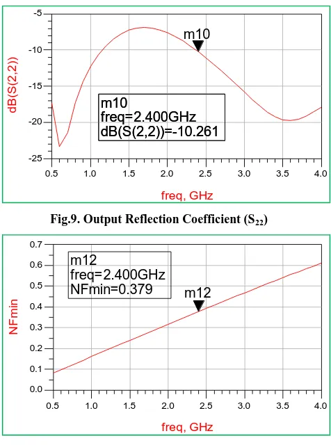
[image:3.595.74.495.289.590.2]For the proposed LNA shown in Fig.4, simulation results are shown in Fig. 5 to 10. The designed low noise amplifier offers forward gain S21 > 15 dB, input return loss S11 < - 15 dB, output return loss S22 < -10 dB and minimum noise figure NFmin < 0.38 dB, for the frequency range of 2 GHz to 3 GHz which are shown in Fig.5, Fig.7, Fig.9 and Fig.10 respectively . The Stability Factor plot is shown in Fig.8. The Stability Factor K > 1 for 2 GHz to 3 GHz which indicates that LNA is unconditionally stable in this frequency range.
37
m7
freq=
dB(S(2,1))=15.227
2.400GHz
1.0 1.5 2.0 2.5 3.0 3.5
0.5 4.0
6 8 10 12 14 16
4 18
freq, GHz
d
B
(S
(2
,1
))
Readout
m7
m7
freq=
dB(S(2,1))=15.227
2.400GHz
Fig.5. Forward Gain (S21)
m8 freq=
dB(S(1,2))=-20.131 2.400GHz
1.0 1.5 2.0 2.5 3.0 3.5
0.5 4.0
-50 -40 -30 -20
-60 -10
freq, GHz
d
B
(S
(1
,2
))
Readout m8
m8 freq=
[image:4.595.51.553.64.729.2]dB(S(1,2))=-20.131 2.400GHz
Fig.6. Isolation (S12)
m9
freq=
dB(S(1,1))=-15.082
2.400GHz
1.0 1.5 2.0 2.5 3.0 3.5
0.5 4.0
-15 -10 -5
-20 0
freq, GHz
d
B
(S
(1
,1
))
m9
m9
freq=
dB(S(1,1))=-15.082
2.400GHz
Fig.7. Input Reflection Coefficient (S11)
1.0 1.5 2.0 2.5 3.0 3.5
0.5 4.0
0.7 0.8 0.9 1.0
0.6 1.1
freq, GHz
K
m11
m11 freq= K=1.009
[image:4.595.314.552.68.388.2]2.400GHz
Fig.8. Stability Factor K
m10
freq=
dB(S(2,2))=-10.261
2.400GHz
1.0 1.5 2.0 2.5 3.0 3.5
0.5 4.0
-20 -15 -10
-25 -5
freq, GHz
d
B
(S
(2
,2
))
Readout
m10
m10
freq=
dB(S(2,2))=-10.261
2.400GHz
Fig.9. Output Reflection Coefficient (S22)
1.0 1.5 2.0 2.5 3.0 3.5
0.5 4.0
0.1 0.2 0.3 0.4 0.5 0.6
0.0 0.7
freq, GHz
N
F
m
in
Readout
m12
m12
freq=
[image:4.595.54.294.70.752.2]NFmin=0.379
2.400GHz
Fig.10. Minimum Noise Figure
Table 1. LNA performance summary with comparisons of published works
[8] [9] [10] Our
Work
Frequency (GHz)
2.40 2.40 2.45 2.40
Supply Voltage (V)
1.2 1.5 0.9 3.0
Gain (dB) 13 21.4 15.3 15.2
Noise Figure (dB)
3.6 5.2 3.34 0.38
Input Reflection (dB)
-13.1 -19.0 -16.5 -15.1
Output Reflection (dB)
-11.5 -- -- -10.2
Isolation(dB) -- -- -- -20.1
6.
CONCLUSIONS
[image:4.595.308.549.424.686.2] [image:4.595.303.549.425.685.2]38 by the proposed methodology achieves up to 15 dB power
gain with a suppressed NF as low as 0.38 dB and provides good input and output matching over 2 GHz to 3 GHz. A 2.4 GHz single stage low noise amplifier is used in IEEE 802.11b and 802.11g standards for wireless local area network (WLAN).Most popular application is Bluetooth. We can also use the designed LNA for the purpose of RF Transceiver systems [5-6, 11]. This can also suitable for the switching circuits.
7.
ACKNOWLEDGMENTS
The authors would like to thank Dr. Priyanka Jain, Assistant Professor, Department of Electronics & Communication, Delhi Technological University, New Delhi for her support and encouragement.
8.
REFERENCES
[1] Avago Technologies Datasheet, “ATF-54143 Low Noise Enhancement Mode Pseudomorphic HEMT in a Surface Mount Plastic Package,” Avago Technologies, USA, Tech. AV01- 0602EN August 5, 2008.
[2] G. Gonzalez (1997),“Microwave Transistor Amplifier: Analysis and Design”, 2nd Edition, Upper Saddle River, NJ: Prentice – Hall Inc. 217, 294-303.
[3] Yazid Mohamed, Norsheila Fisal and Mazlina Esa “Simulation Study of Broadband LNA for Software Radio Application” June 2000.
[4] Joseph C. Bardinand, Sander Weinreb, “A 0.1 GHz to 5 GHz cryogenic SiGe MMIC LNA,” IEEE Microwave and Wireless Components Letters, vol. 19, no. 6, June 2009.
[5] Viranjay M. Srivastava, K. S. Yadav, and G. Singh, “Analysis of double gate CMOS for double-pole
four-throw RF switch design at 45-nm technology,” J. of Computational Electronics, vol. 10, no. 1-2, pp.229-240, June 2011.
[6] Viranjay M. Srivastava, K. S. Yadav, and G. Singh, “Design and performance analysis of double-gate MOSFET over single-gate MOSFET for RF switch,” Microelectronics Journal, vol. 42, no. 3, pp.527-534, March 2011
[7] D.M.Pozar, “Microwave and RF Design of Wireless System” 3rd Edition: John Wiley & Sons Inc, 2001.
[8] M. E. Kaamouchi, M. S. Moussa, P. Delatte, G. Wybo, A. Bens, J.-P.Raskin, and D. Vanhoenacker-Janvier, “A 2.4 GHz fully integrated ESD-protected low-noise amplifier in 130-nm PD SOI CMOS technology,” IEEE Trans. Microwave Theory Tech., vol. 55, pp. 2822-2831, Dec. 2007.
[9] A. V. Do, C. C. Boon, M. A. Do, K. S. Yeo, and A. Cabuk, “A subthreshold low-noise amplifier optimized for ultra-low-power applications in ISM band,” IEEE Trans. Microwave Theory Tech., vol. 56, pp. 286-292, Feb. 2008.
[10]M. Cimino, H. Lapuyade, Y. Deval, T. Taris, and J.-B. Begueret, “Design of a 0.9 V 2.45 GHz self-testable and reliability-enhanced CMOS LNA,” IEEE J. Solid-State Circuits, vol. 43, pp. 1187-1194 May 2008.
[11]Yongguang Lu; Shu-hui Yang; Yinchao Chen; , "The design of LNA based on BJT working on 2.2–2.6GHz," Signal Processing Systems (ICSPS), 2010 2nd International Conference on , vol.1, no., pp.V1-143-V1-