Hone)'\Nell
MULTICS
DIFFERENCES
MANUAL
DPS 8
70/M
HONEYWELL CONFIDENTIAL
&
PROPRIETARYTtlil document and ttta 'ntonna"on oonta'nec:I here'n a" confldenUal to and the pro.,y of Honaywa" Informltlon Sylleml, Inc. Ind I,. med • . . Uabla only to HOMywaU emploY"' 'or the to .. purpo . . 0' OOMuctlno Honeywall'l bU"neal. Tttl. documlnt, any copy thereof Ind ttt. , 'n'Of'Ift8t'Oft con'aln_ heN'n 1,..11 be maintained In .tnet .. t oonfldeftOe; ... 11 not be coP'_ In ."011 or 'n Plrt ,XClpt . . aut"ortzed by''''
"""or-',
manager; and 11\111 not be d'lOlolId or dtltrtbutecf (a) to ...,.. "'0 ... not Honeywa" employeel, or (b) to Honeyw.1I employ ... for wftOm IUC" 'n'O""ltlon I. "-" ,...ury .n connection wit" 'N'r ""Oned _penllbn" .... Upon l"IIQutlt. or whln ttta employ .. Inoo ... on of ." •• documant no lono., hal n _ for thl c:tocument for '''a 8<"o,'* Honeywell purpou. ttt •• document and any coP," t"areo.f' ... be retumed to tM amploy . . ·• manager. Thare 1",11 be no IXCIC)t.on. to ttte terml and condltlonl I" fOlth h ... n axcept al luthorlzld In -nUnO by the NePOn.,b .. Honaywell Vice p,..'dent.
WCPU68LA DIFFERENCE MANUAL
PREFACE
The purpose of this manual is to describe at a high level the hardware differences that are unique to the (WCPU68LA) DPS 8/70M
processors relative to the current (WDPS68~m/SA;MB/SB) L68
processors. Because this manual describes the hardware
differences at a high level it presumes that the reader has a
thorough knowledge of the L68 processor. Some explana tions may
require the use of the Logic Block Diagrams.
This manual descr ibes changes made
changes were made to reduce the
increase the processor speed.
to the CU and APU. These
processor board count and
These CU and APU changes resulted in minor changes to a few of the processor instructions.
The board count in the CU was reduced, a hardware cache added and instruction buffer management changed. count in the APU was reduced and the PTW and SDW memories increased to 64 words each.
controlled The board associative
The following notice is provided in accordance with the United States Federal Communications Commission's (FCC) regulations.
Warning: This equipment generates, uses, and can radiate radio frequency energy and if not installed and used in accordance with the instructions manual, may cause interference to radio communications. It has been tested and found to comply with the limits for a Class A computing device pursuant to Subpart J of Part 15 of FCC Rules, which are designed to provide reasonable protection against such interference when operated in a commercial environment. Operation of this equipment in a residential area is likely to cause interference in which case the user at his own expense will be required to take whatever measures !T1ay be required to correct the inteference.
REV DATE
A AUGUST
ISSUED 1983
58009997-014
RECORD OF REVISIONS
AUTHORIZATION
PHAFPD951
IF
PAGES AFFECTED
58009997-040 58009997-014, IF 58009997-033, IF 58009997-001, IF
58009997-017, 1 thru 4F 58009997,019, IF
TABLE OF CONTENTS
Binder, A-size, 3-ring, 1-1/2 inch •••••••••••••• 58009875-010
Spine ••••••••••••••••••••••••••••••••••••••••••• 58009997-033 Title Page •••••••••••••••••••••••••••••••••••••• 58009997-040 Record of Revisions ••••••••••••••••••••••••••••• 58009997-014 Preface ••••••••••••••••••••••••••••••••••••••••• 58009997-019 Table of Contents ••••••••••••••••••••••••••••••• 58009997-001 Manual Contents ••••••••••••••••••••••••••••••••• 58009997-017
1.0 1.1 1.1.1 1.1.2 1.1.3 1.1.4 1.1.5 1.2 1.2.1 1.2.2 1.2.3 1.2.4 1.2.5 2.0 3.0 3.1 3.2 3.3 3.3.1 3.3.2 3.4 3.4.1 3.4.2 3.4.3 3.5 3.6 3.7 3.8 3.9 3.10 3.11 3.12 3.13 3.14 3.14.1 3.14.1.1 3.14.1.2 3.14.1.3 3.14.1.4 3.14.1.5 3.14.1.5.1
MANUAL CONTENTS
INTRODUCT ION. • • • • • • • • • • • • • • • • • • • • • • • • • • • • • • • • • • • •• 1 PROCESSOR UNIT FUNCTIONS •••••••••••••••••••••••••• 1 Operations Unit (OU) •••••••••••••••••••••••••••••• 1 Decimal Unit (DU) ••••••••••••••••••••••••••••••••• 1 Control Unit (CU) ••••••••••••••••••••••••••••••••• 1 Append Unit (APU) ••••••••••••••••••••••••••••••••• 2 Associative Memory Assembly ••••••••••••••••••••••• 3 DEFINITIONS OF NOTATION AND SyMBOLS ••••••••••••••• 3 Main Memory Address ••••••••••••••••••••••••••••••• 3 Index Values •••••••••••••••••••••••••••••••••••••• Abbreviations and Symbols ••••••••••••••••••••••••• Register Positions and Contents ••••••••••••••••••• Other Symbol s •••••••••••••••••••••••••••••••••••••
4 4
5 5 DIFFERENCES UNIQUE TO DPS 8 PROCESSORS •••••••••••• 6
DIFFERENCES UNIQUE TO LEVEL 68/DPS 8 •••••••••••••• 6
PROCESSOR NUMBERS, PROCESSOR TO SCU PORTS ••••••••• 7 ASSOCIATIVE MEMORIES •••••••••••••••••••••••••••••• HARDWARE CONTROLLED CACHE ••••••••••••••••••••••••• Summary ••••••••••••••••••••••••••••••••••••••••••• Details ••••••••••••••••••••••••••••••••••••••••••• 7 8 8 9 HISTORY REGISTERS ••••••••••••••••••••••••••••••••• 10 CU History Register Format •••••••••••••••••••••••• 11 OUIDU History Register Format ••••••••••••••••••••• 11 Appending Unit History Register (APUHR) Format •••• 13 MODE SWITCH... 14 MODE REGISTER (MR) FORMAT ••••••••••••••••••••••••• 15 CACHE MODE REGISTER (CMR) FORMAT •••••••••••••••••• 17 FAULT REGISTER FORMAT ••••••••••••••••••••••••••••• 19 SEGMENT DESCRIPTOR WORD (SDW) FORMAT •••••••••••••• 22 PAGE TABLE WORD (PTW) FORMAT •••••••••••••••••••••• 25 SEGMENT DESCRIPTOR WORD ASSOCIATIVE MEMORY
(SDWAM) FORMAT... 26 PAGE TABLE WORD ASSOCIATIVE MEMORY (PTWA}l)
FORMAT. • • • • • • • • • • • • • • • • • • • • • • • • • • • • • • • • • • • • • • • • • •• 30 ID PROM... 32 INSTRUCTIONS AFFECTED BY CHANGES •••••••••••••••••• 33 INSTRUCTIONS AFFECTED BY PROCESSOR NUMBERS
PROCESSOR TO SCU PORT CHANGES ••••••••••••••••••••• 33 reel Read Calendar Clock •••••••••••••••••••••••••• 33 rmcm Read Memory Controller Mask Register ••••••••• 34 smcm Set Memory Controller Mask Register •••••••••• 35 smic Set Memory Controller Interrupt Cells •••••••• 36 rsw Read Switches ••••••••••••••••••••••••••••••••• 37 Configuration Switch Data ••••••••••••••••••••••••• 38
3.14.2 3.14.2.1 3.14.2.2 3.14.3 3.14.4 3.14.4.1 3.14.4.2 3.14.4.3 3.14.5 3.14.5.1 3.14.5.2 3.14.5.3 3.14.5.4 4.0 4.1 4.2 5.0 5.1 5.2 6.0 6.1 6.2 6.3 6.3.1 6.3.2 7.0 7.1 7.1.1 7.2 7.2.1 7.2.2 7.2.3 7.2.4 7.2.5 7.2.6 7.2.7 7.2.8
MANUAL CONTENTS (CONT.)
Instructions Affected by History Registers ••••••• 40 lcpr Load Control Processor Registers •••••••••••• 40 scpr store Control Processor Registers ••••••••••• 41 scu Store Control Unit ••••••••••••••••••••••••••• 42 Instructions Affected by 8K Cache •••••••••••••••• 48 stacq Store A Conditional on Q ••••••••••••••••••• 48 camp Clear Associative Memory Page ••••••••••••••• 49 cams Clear Associative Memory Segments ••••••••••• 50 Instructions Affected by Associative Memory
Changes •••••••••••••••••••••••••••••••••••••••••• 51 sptp Store Page Table Pointer •••••••••••••••••••• 51 sptr Store Page Table Registers •••••••••••••••••• 52 ssdp Store Segment Descriptor Pointer •••••••••••• 53 sstr store Segment Descriptor Register ••••••••••• 54
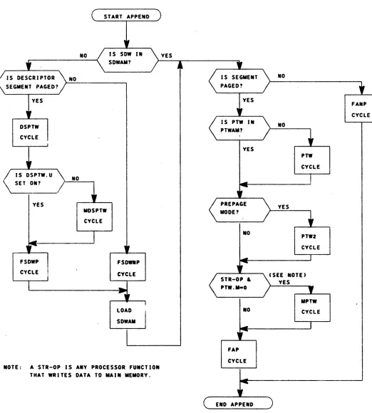
VIRTUAL ADDRESS FO~lATION •••••••••••••••••••••••• 56
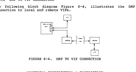
DEFINITION OF VIRTUAL ADDRESS •••••••••••••••••••• 56 TYPES OF VIRTUAL ADDRESS FORMATION ••••••••••••••• 56 ADDRESS APPENDING •••••••••••••••••••••••••••••••• 58 UNPAGED DSBR. U=l ••••••••••••••••••••••••••••••••• 62 PAGED DSBR.U=O ••••••••••••••••••••••••••••••••••• 63 DPS a/70M PHYSICAL HARDWARE •••••••••••••••••••••• 66 LOGIC BOARD BACKPANEL COMPARISON ••••••••••••••••• 66 DPS a/70M BLOCK DIAGRAM •••••••••••••••••••••••••• 67 DIAGNOSTIC MAINTENANCE PANEL (DMP) FEATURES •••••• 68 DMP to VIP Connection •••••••••••••••••••••••••••• 72 DMP to DPU Connection •••••••••••••••••••••••••••• 73 BASIC OPERATION •••••••••••••••••••••••••••••••••• 74 INSTRUCTION STREAM SEQUENCE •••••••••••••••••••••• 74
Transfer Sequences ••••••••••••••••••• ~ ••••••••••• 74
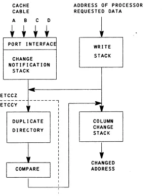
8K CACHE ••••••••••••••••••••••••••••••••••••••••• 76 Operation Description •••••••••••••••••••••••••••• 76 Directory and Cache Addressing ••••••••••••••••••• 79 Least Recently Used Hardware ••••••••••••••••••••• 81 F / E Bit s •••••• _. • • • • • • • • • • • • • • • • • • • • • • • • • • • • • • • • •• 81 LRU Bits ••••••••••••••••••••••••••••••••••••••••• 81 Duplicate Cache Directory •••••••••••••••••••••••• 82 Cache Data Store ••••••••••••••••••••••••••••••••• 84 Cache Hit Timing ••••••••••••••••••••••••••••••••• 84
7.2.9 7.2.10 7.2.11 7.2.12 7.2.13 7.3 7.4 7.5 7.6 7.6.1 7.6.2 7.6.3 7.6.3.1 7.6.4 7.7 7.7.1 7.7.2 7.7.3 7.7.4 7.7.5 7.8 7.9 7.9.1 7.10 7.11 7.12
FIGURE NO. 5-1 5-2 5-3 6-1 6-2 6-3 6-4 6-5
MANUAL CONTENTS (CONT.)
Cache Miss Timing •••••••••••••••••••••••••••••••• 86 ETCCC Board •••••••••••••••••••••••••••••••••••••• 88 ETCCD Board •••••••••••••••••••••••••••••••••••••• 90 ETCCZ Board •••••••••••••••••••••••••••••••••••••• 92 ETCCY Board •••••••••••••••••••••••••••••••••••••• 94 INSTRUCTION BUFFER MANAGEMENT •••••••••••••••••••• 94 ETCBG BOARD... 97 ASSOCIATIVE MEMORy ••••••••••••••••••••••••••••••• 99 PAGE TABLE WORD ASSOCIATIVE.MEMORY (PTWAM) ••••••• 101 PTWAM Directory •••••••••••••••••••••••••••••••••• 101 F/E Bit •••••••••••••••••••••••••••••••••••••••••• 101 LRU Array •••••••••••••••••••••••••••••••••••••••• 102 Level Usage Decode ••••••••••••••••••••••••••••••• 103 PTWAM Data Storage ••••••••••••••••••••••••••••••• 103 SECTOR DESCRIPTOR WORD ASSOCIATIVE.MEMORY
(SDWAM} •••••••••••••••••••••••••••••••••••••••••• 104 SDWAM Directory •••••••••••••••••••••••••••••••••• 104 SDWAM Associative Memory Data Storage •••••••••••• 106 SDW AM Timing ••••••••••••••••••••••••••••••••••••• 1 0 8 ETMPA Board •••••••••••••••••••••••••••••••••••••• 109 ETMPB Board (ESN Generation) ••••••••••••••••••••• 110 ETMBA BOARD (ADDRESS PREPARATION) •••••••••••••••• 115 POINTER REGISTER ••••••••••••••••••••••••••••••••• 117 ETf,lPH Board •••••••••••••••••••••••••••••••••••••• 119 ZDO - APU BUS •••••••••••••••••••••••••••••••••••• 121 APPENDING UNIT OPERATOR CHARTS ••••••••••••••••••• 124 GROUP 6 FAULTS ••••••••••••••••••••••••••••••••••• 136
LIST OF ILLUSTRATIONS DESCRIPTION
APPENDING UNIT OPERATION FLOWCHART ••••••••••••••• 61 ADDRESS PREPARATION DESCRIPTOR SEGMENT UNPAGED ••• 62 ADDRESS PREPARATION DESCRIPTOR SEGMENT PAGED ••••• 64 DPS 8/70M BLOCK DIAGRAM •••••••••••••••••••••••••• 67
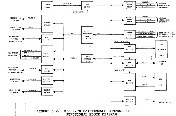
DPS 8/70 MAINTENANCE CONTROLLER FUNCTIONAL BLOCK
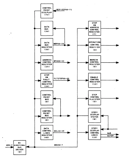
DIAGRAM. • • • • • • • • • • • • • • • • • • • • • • • • • • • • • • • • • • • • • • • •• 69 DPS 8/70 CPU INTERFACE LOGIC ••••••••••••••••••••• 71 DMP TO VIP CONNECTION •••••••••••••••••••••••••••• 72 DMP TO DPU CONNECTION •••••••••••••••••••••••••••• 73
FIGURE NO. 7-1
7-2 7-3 7-4 7-5 7-6 7-7 7-8 7-9 7-10 7-11 7-12 7-13 7-14 7-15 7-16 7-17 7-18 7-19
LIST OF ILLUSTRATIONS (CONT.)
DESCRIPTION
CACHE SUBSYSTEM BLOCK DIAGRAM •••••••••••••••••••• 77 DIRECTORY AND CACHE ADDRESSING ••••••••••••••••••• 80 DUPLICATE DIRECTORY BLOCK DAIGRAM •••••••••••••••• 83 CACHE ACCESS PATH AND CACHE HIT TIMING ••••••••••• 85 CACHE MISS TIMING •••••••••••••••••••••••••••••••• 87 ETCCC BLOCK DIAGRAM •••••••••••••••••••••••••••••• 89 ETCCD BLOCK DIAGRAM •••••••••••••••••••••••••••••• 91 ETCCZ BLOCK DIAGRAM •••••••••••••••••••••••••••••• 93 ETCCY BLOCK DIARGRAM ••••••••••••••••••••••••••••• 95 INSTRUCTION BUFFER MANAGEMENT •••••••••••••••••••• 96 ETCBG BLOCK DIAGRAM •••••••••••••••••••••••••••••• 98 ETCPB BOARD SDW DIRECTORY, F/E.AND LRU ARRAY ••••• I05 SDW LOAD SEQUENCE •••••••••••••••••••••••••••••••• I08 ETMPA BLOCK DIAGRAM •••••••••••••••••••••••••••••• 111 ETMPB BLOCK DIAGRAM •••••••••••••••••••••••••••••• 112 EFFECTIVE SEGMENT GENERATION FLOWCHART ••••••••••• 113 ETMBA BLOCK DIAGRAM •••••••••••••••••••••••••••••• 116 ETMPH BLOCK DIAGRAM •••••••••••••••••••••••••••••• 120 COMPLETE APPENDING UNIT OPTION FLOWCHART ••••••••• 124
LIST OF TABLES
TABLE NO. DESCRIPTION
5-1 APPENDING UNIT CYCLE DEFINITIONS ••••••••••••••••• 60
7-1 ZDO - APU BUS •••••••••••••••••••••••••••••••••••• 122
1.0 INTRODUCTION
The purpose of this manual is to descr ibe at a high level the hardware differences that are unique to the level (WCPU68LA) DPS 8/70M processors relative to current level (WDPS68MA/SA;MB/SB) L68 processors. This new 68/DPS 8 processor will support MULTICS and GCOS III in the emulation mode or GCOS III via manual switch setting.
1.1 PROCESSOR UNIT FUNCTIONS
The general major functions of each principal logical unit of the processor are listed below and the differences are described in subsequent sections of this manual.
1.1.1 OPERATIONS UNIT (OU) This unit
does-o Fixed and floating-binary operations o Shifting
o Boolean operations
This unit is unchanged. 1.1.2 DECIMAL UNIT (DU) This unit
does-o Decimal arithmetic
o Character and bit string operations
This unit is unchanged. 1.1.3 CONTROL UNIT (CU)
This unit
does-o Address modification
o Controls mode of operat'ion (privileged, normal, etc.) o Interrupt recognition
o Decodes instruction and indirect words
o Controls timer register loading and decrementing
o Contains cache memory
This unit has been considerably changed to reduce the MULTICS processor board count and to take advantage of the performance improvements made possible by cache memory.
The following characteristics change this unit.
o Improved processor performance
o Cache integral part of CU
o Automatic cache clearing and 8K word cache size
o Size and contents of history registers
o Decrease of number of processor to SCU ports from
8 to 4
o PROM to store ID codes and identify separately
priced software
o Maintenance panel interface
1.1.4 APPEND UNIT (APU)
This
unit-0 Controls data input/output to main memory
0 Performs main memory selection and interlace
0 Does address appending
0 Controls fault recognition
0 Interfaces with cache
The append unit has been changed to take advantage of the performance improvement made to the Control Unit and Associative Memory.
The following characteristics change this unit.
o Improved processor performance
o Size of history registers
o Decrease in number of CPU to SCU ports from 8 to 4
a Configuration panel interface
1.1.5 ASSOCIATIVE MEMORY ASSEMBLY
The Associative Memory Assembly consists of a set of registers
used to hold pointers to Page Table Words (PTW) and Segment
Descriptor Words (SDW) that have recently been used to develop
absolute address. The number of SDWAM and PTWAM registers have
been increased to 64 from 16.
1.2 DEFINITIONS OF NOTATION AND SYMBOLS
The following notations and symbols are used in this manual:
1.2.1 MAIN MEMORY ADDRESSES
Y =
Y
=
Y-pair =
Y-blockn =
Y-charnk =
an 18-bit computed address as generated
during address preparation.
a 24-bit
instruction preparation complete.
main memory address of the
operand after all address
(including appending) is
a pair of main memory locations with
successive addresses, the smaller address
being even. When Y is even, it designates
the pair Y (even), Y+li and when it is odd,
the pair Y-I, Y (odd). The main memory
location with the smaller (even) address
contains the most significant part of a
double-word operand or the first of a pair of instructions.
a block of main memory loca tions of 4- , 8-,
16-, or 32-word extent. For a block of
n-word extent, the processor forces Y-blockn
to a 0 modulo
n
address and performs addressincrementing through the block accordingly,
stopping when the address next reaches a
value 0 module
n.
a character or string of characters in main
memory of character size
n
bits as describedby the kth operand descr iptor.
n.
isspecified by the data type field of operand
descriptor
k
and may have values 4, 6, or 9.Y-bitk
=
a bi t or str ing of bi ts in main memory as described by the kth operand descriptor.1.2.2 INDEX VALUES
When reference is made to the elements of a string of characters or bits in main memory, the notation shown in "Register Position and Contents" below is used. The index used to show traversing a
string of extent
n
may take any of the values in the interval(l,n) unless noted otherwise. The elements of a main memory
block are traversed explicitly by using the index as an addend to the given block address, (e.g •• Y-block8+m and Y-block4+2m+l). 1.2.3 ABBREVIATIONS AND SYMBOLS
A ARn AQ BAR C () CA DSBR DSBR.ADDR DSBR.BND DSBR.STACK DSBR.U E EA EAQ ERN ESN FCT HOLD IC IR PPR PPR.PRR PPR.PSR PPR.IC PPR.P PRn PRn.RNR PRn.SNR PRn.WORDNO PRn.CHAR PRn.BITNO PRR PSR
Accumulator register
Address register n (n
=
0, 1, 2, ••• ,7) Combined accumulator-quotient register Base address register"Contents of" Computed address
Descriptor segment base register Address field of DSBR
Bound field of DSBR
Stack base field of DSBR Unpaged flag of DSBR Exponent register
Combined exponent-accumulator register
Combined exponent-accumulator-quotient register Effective ring number
Effective segment number
Fault counter-counts instruction Holding register
Instruction counter Indicator register
Procedure pointer register Procedure ring register of PPR Procedure segment register of PPR
Instruction counter register of PPR ( same as IC above)
Privileged flag of PPR
Pointer register n (n
=
0, 1, 2, ••• ,7) Ring number register of PRnSegment number register of PRn Word address register of PRn
Character address register of PRn Bit offset register of PRn
Procedure ring register Procedure segment register
Q
PTWAM SDWAM RALR TPR TPR.CA TPR.TRR TPR.TSR TPR.TBR TR
TRR Xn
Z
1.2.4
Quotient register
Page table word associative memory
Segment descriptor word associative memory Ring alarm register
Temporary pointer register
Computer address register of TPR (same as CA above) Temporary ring register of TPR
Temporary segment register of TPR Temporary bit register of TPR Timer register
Temporary ring register
Index register n (n
=
0, 1, 2, ••• , 7)Temporary pseudo-result of a nonstore comparative operation
REGISTER POSITIONS AND CONTENTS
In the definitions that follow, "R" stands for any registers listed above as well as for main memory word-pairs, word-blocks, and bit- or character-strings.
of the words,
Ri The ith bit, character, or byte position of R
R(i) The ith register of a set of n registers named R
Ri,j The bit, character or byte positions i through j or R
CCR) The contents of the full register R
C(R) The contents of the ith bit, character, or byte of
R
C (R)' 1.,J .
xx ••• x
The contents of the bits, characters, or bytes i through j of R
A string of binary bits (O's or l's) of any necessary length
When the descr iption of an instruction specifies a change for a part of a register or main memory location, i t is understood that the part of the register or main memory location not mentioned remains unchanged.
1.2.5 OTHER SYMBOLS
-) replaces
:: compare with
&
·
·
XXX
n**m
X
/
·
.
·
.
• • • •C(R)modn
the Boolean connective AND the Boolean connective OR
the Boolean connective NON-EQUIVALENCE (or EXCLUSIVE OR)
the logical inverse (ones complement) of the quantity XXX
not equal
indicates an exponent (n and m are integers); for example, the fifth power of 2 is represented as 2**5. multiplication; for example, C(Y) times ceQ) is
represented as C(Y) X C(Q).
division; for example, C(Y) divided by C(A) is represented as C(Y) / C(A).
concatenation; for example, string 1:: string 2.
the absolute value of the value between vertical bars
(no algebraic sign). For example the absolute, value
of C(A) plus C(Y) is represented as: C(A) + C(Y) •
A coined notation for remaindering or modulo arithmetic; for example C(REG) modulo 9 is represented as C(REG)mod9.
2.0 DIFFERENCES UNIQUE TO DPS 8 PROCESSORS
The hardware for all four processor ports is buil t in to and is
functional in all processors. In pre-DPS 8 processors, the port
boards were separately-installable options. The 8K word cache is built into all processors.
When operating in GeOS III mode (mode swi tch set for GCOS), the system is functionally identical to Level 66/DPS 8 (NON NSA).
3.0 DIFFERENCES UNIQUE TO LEVEL 68/DPS 8
This section lists differences from MULTICS systems which are unique to the Level 68/DPS 8 system.
3.1 PROCESSOR NUMBERS, PROCESSOR TO SCU PORTS
I The maximum number of processors designated per system is
extended from 4 to 8. Processor numbers will be designated by
three bi ts. The maximum number of SCU· s per system is reduced
from 8 to 4. The previous recogni tion of processor ports E, F,
G, and H is dropped.
Several instructions which specified the processor by C(TPR.CA)1-2(see Section 1.2, Definitions of
Symbols) will now ignore bit position O. Port
L68/DPS 8 is specified by C(TPR.CA)1-2.
instructions are:
Op Code Mnemonic Name
633(0) rccl Read Calendar Clock
port selection Notations and selection for
The affected
233 (0) rmem Read Memory Controller Mask Register
451(0) smic Set Memory Controller Interrupt Cells
55~(0) smcm set Memory Controller Mask Register
Processor number will occupy three bits in the control unit data,
bit positions 27-29 of word 2, rather than two bits. The
affected instructions are:
Op Code Mnemonic
657 (0) sell
513 (0) rCll
Name
Store Control Unit Restore Control Unit
The reduction in the number of processor ports and the
rearrangement of data fields in read switches instruction allows elimination of instructions rsw3 and rsw4.
3.2 ASSOCIATIVE MEMORIES
The Segment Descriptor Word and Page Table Word associative
memories are extended to 64 words from 16 words. The 64 word
associative memories are organized as "four level set-associative with LRU replacement.
Existing T&D instructions which loaded the associative memories
are deleted. They are not required for the new T&D tests. The
deleted instructions are:
Op Code Mnemonic
257 (1) 172 (1)
257 (0)
232 (1)
lptp lptr lsdp lsdr
Name
Load Page Table Pointers Load Page Table Registers
Load Segment Descriptor Pointers Load Segment Descriptor Registers
The T&D instructions which stored contents of the associative
memory are modified to accommodate the increase of size to 64
words. These are:
Op Code Mnemonic
557 (1) 154 (1)
557 (0)
254 (0)
sptp sptr ssdp ssdr
_ _ _ _ _ _ ----'Nlr.L:a=.lm~e~.~ _ _ _ _ _ _
Store Page Table Pointers store Page Table Registers
store Segment Descriptor Pointers store Segment Descriptor Registers
3.3 HARDWARE-CONTROLLED CACHE
3.3.1 SUMMARY
The Level 68/DPS 8 processor has an 8K word hardware controlled
cache. The design eliminates the need for certain cache clears
and cache bypass modes that were required in the previous 2K word software controlled cache.
The requirement for coexistence of the 2K cache with the 8K cache in a roul tiprocessor system has led to the introduction of an
additional cache bypass control. This is provided in the
processor's cache mode register. This will permit coexistence
without requiring a change in the 2K cache processor or
restricting the types of multiple memory connections.
A synchronizing function, whose purpose is to ensure integrity of
gated shared data, is provided in the instruction repertoire.
This function is added to the stc2 and stacq instructions. This
addition is needed to support 8K cache processors in
multiprocessor, multi-SCU systems.
An additional performance improvement involves the group of
read-alter-rewrite instructions. These will no longer
automatically bypass cache, as in the 2K cache processor, unless
a cache bypass mode is in effect. This cache mode is· totally
controlled by the cache bypass bit, SDW.C, in the segment
descriptor.
Full utilization of the performance capabilities require changes
to MULTICS software. Among these are replacement of open gate
instructions with stc2 or stacq, and changes to SDW.C to specify
cache use instead of bypass. Software considerations must also
be given to the 2K-8K coexistence, and the eventual phasing out of this requirement as migration from 2K to 8K cache processors occurs.
3.3.2 DETAILS
The cache bypass option in the segment descriptor word is
retained. An overriding bypass enable, bit 68 of the cache mode
register is added. The cache mode is set as follows:
SDW.C
Use Cache
Bypass Cache
Bypass Cache
Clm
x
Bypass Cache
Use Cache
RESULTANT CACHE MODE
Use Cache
Bypass Cache
Use Cache
All close gate instructions, ldac, ldqc, stac, stacq, and sznc
will automatically bypass cache. Two features are added to
ensure integrity of gated shared data; one is added during the
close gate operation and the other during the open gate
operation. The instruction following the close gate instruction
will bypass cache if the instruction is a read or a
read-alter-rewrite. The open gate operation must be performed
with either a stc2 or stacq which includes the synchronizing
function. The synchroniz ing function forces the processor to
delay the open gate operation until it is notified by the SCU
that write completes have occurred and write notifications
requesting cache block clears have been sent to the other
processors for all write instructions that the processor has previously issued.
Read-alter-rewrite instructions will no Ionger automatically
bypass cache. Cache behavior for these instructions is
determined fully by SDW. C. If the bypass cache mode is set,
these instructions will bypass cache and issue
read-Iock-write-unlock commands to memory. If a cache directory
match occurs, the location is cleared.
All accesses to memory by SDW and PTW associative memory hardware
will continue to bypass cache. Operations used will be reads for
SDWs, read-alter-rewrites with lock for PTWs and setting the page used bit, and writes for setting the page modified and used
bits. For writes, the hardware will also disable the key line so
that the SCD lock is honored. This is consistent wi th dynamic
PTW modi fica tion by software which also bypasses cache and uses read-alter-rewrite instructions.
The instructions which cleared the associative memories and also cleared cache or selective portions of cache are changed to
eliminate the cache clear function. Bit C (TPR.CA)15 is
ignored. These instructions will also include disable/enable
capabilities for each quarter of the associative memories.
The associative memory replacement is LRUi (Least Recently Used);
this is also reset upon a camp or cams so that repeatable
behavior occurs under test conditions. Cache mode register bit
56, which had previously controlled cache bypass for operands is
disregarded. All other cache control bits are continued.
However, maintenance panel cache control function is restricted to cache half enable/disable functions.
The cache memory replacement method is also LRU.
3.4 HISTORY REGISTERS
On prior Level 66 systems, the processor history registers were
16 instructions or steps deep. This has proved to be less than
desired. These registers are now implemented 64 steps deep in
the DPS 8
cpu.
Theau
and DU registers are combined into a72-bit register which is pulled in a single access. Many of the
OU and DU bits were rarely used and were eliminated.
As an aid to software debug, a capability for history register strobe on "transfer" was added.
In order to read the history registers and place them in the
store, the scpr instruction must be used. The TAG field of the
scpr indicates which of the 64 register groups will be stored,
the CU group, the OU/DU group, the APU group. In order to store
a full group of 64 registers, an scpr instruction must be
executed by the processor 64 times in succession.
The TAG field code is shown below:
Select CU History Register - TAG field
=
010000 (20)aSelect OU/DU History Register - TAG field
=
100000 (40)aSelect APU History Register - TAG field
=
000000 (OO)aThe lcpr instruction with the tags of 038 and 078 shall load all
four groups of history registers with zero's and one's,
respectively.
3.4.1 CU HISTORY REGISTER FORMAT
00 01 02 03 04 05 06 07 08 09 10 11 12 13 14 15 16 17 18-35 36-59 60-64 65 66 67 68 69 70 Field FPIA FPOA DRIW FSIW FPOT FPON DRAW FSAW XDE XDO FIC RPTS PORTF MATCHF XIP/ADR FLT/ADR MASTER MODE Op code and Tag
Function
Prepare Instruction Address Prepare Operand Address Request Indirect Word Restore Indirect Word Prepare Operand Tally Prepare Operand Next Read-Alter Word
store Read-Alter Word Remember TRA/GO
Execute Double from Even Execute Double from Odd
Odd Instruction from Current Pair Repeat Flag
Memory Cycle Went to Port
Memory Cycle went to Cache/Direct Prepare Interrupt Address
Prepare Fault Address Processor in Master Mode A copy of bits 18-35 of the
executed.
instruction being 24-Bit Real Memory Address
Command Register A copy of the Lines A-E)
FXEC-INT RB-INS-FETCH RB-CACHE-RD RB-NONMCACHE RB-STORE PC-BUSY
Processor Command Execute Interrupt Instruction Fetch Cache Read
Memory Read Store
Port Busy
Register (Command
Cycle
3.4.2 OU/DU HISTORY REGISTERS FORMAT
B.it
00 01 02 Field FANDLI FANDL2 FANSTR FunctionAlpha-Numeric Load Desc. 1 Alpha-Numeric Load Desc. 2 Alpha-Numeric Store
HONEYWELL CONFIDENTIAL & PROPRIETARY
03 04 05 06 07 08 09 10 11 12 13 14 15 16 17 18 19 20 21 22 23 24 25 26 27 28 29 30 31 32 33 34 35 36-53 54-62 63 64 65 66 67 68 69 70 71 FLDWRTI FL Dl-IR T2 FNLDI FNLD2 FEND-SEQ FDUD FGSTR DEND-SEQ (NINE (SIX (FOUR (BIT (WORD {PTRAOO (PTRAOI (PTRA02 FPOP GFGEAA-M FGLDPl-2 FGEMA-E FGBDABC FGSPl-5 FSWEQ FGCH DFRST (EXH FGADD FINTRPTD DCODE 0
1
2
3
4
Load-Rewrite Register 1 Load-Rewrite Register 2 Numeric Load Desc. 1 Numeric Load Desc. 2 End Sequence Flag Decimal Unit Idle General Store End of Sequence
9-Bit Character Operation 6-Bit Character Operation 4-Bit Character Operation Bit Operation
Word Operation Select PTR 1 Select PTR 2 Select PTR 3
Prepare Operand Pointer Load Pointer 1+2
Multiply Gates
Binary to Decimal Gates Align Cycles
Character Cycle Exhaust
Add Cycle Interrupted
A copy of the Instruction Counter
A copy of OU Op Code Register - (RSO - RS8) ZERO SIGN CARRY OVFL EOVFL EUFL OFLl4 HEX MODE DTRGO
Indicator Register Indicator Register Indicator Register Indicator Register Indicator Register Indicator Register Indicator Register Indicator Register Transfer Go
C - Data Stored in Complement Form
HONEYWELL CONFIDENTIAL & PROPRIETARY
3.4.3 APPENDING UNIT HISTORY REGISTER (APUHR) FOlUlAT
The contents and number of the APUHRs remain the same, the
contents are repeated here for convenience. The APUHRs are
handled as a rotating queue controlled by the appending unit
history register counter. The counter is always set to the
number of the oldest entry and advances by one for each history register reference (data entry or scpr instruction).
The appending unit history register shows the condition in the appending unit at the end of an address preparation cycle in
append mode. The registers will hold the conditions for the last
16 such address preparation cycles. Entries are made according
to controls set in the mode register •
.Bit
History 0-14 15 16 17 18 19 20 21 22 23 24 25 26 27-28 29 30 31-34 35 Field Register ESN PIAPGBSY PIAOOSB FDSPTW MDSPTW FSOWP FPTW FPTW2 MPTW FANP FAP SDWAMM SDWMF BSY PTWMF MTCHP'IW PTWADOR FLT I I FunctionEffective segment number (TPR.TSR) Instruction fetch across a page boundary
Instruction fetch cycle out of segment boundary
Descriptor segment PTW fetch
Descriptor segment PTW modification SOW fetch from paged descriptor segment
PTVl fetch
PTW+1 fetch (prepaging for certain EIS instructions)
PTW modification
Final address fetch from nonpaged segment
Final address fetch from paged segment
SDWAM match occurred
SDWAM match occurred and used Data Source for ESN
00
=
from PPR.PSR01
=
from PRn.TSR10 = from TPR.SNR
11
=
from TPR.CAPTWAM match occurred and used PTWAM match occurred
(TPR.CA)4,7 Address select for
PTWAM
Access violation or directed fault on this cycle
36-59
60-62 63
64-65
66 67 68-69
70
ADD
TRR
SDWERR SDWLVL
CA PTWERR PTWLVL
FHLD
History Register 12
00-17 18-27 28
29
30-35
36-71
AD DR OPCODE
I
P
TAG
3.5 MODE SWITCH
24-bit absolute main memory address from this cycle
Ring number from this cycle
(TPR.TRR)
Multiple match or parity error in SDWAM
SDWAM Level selected 00
=
A01
=
B10
=
C11
=
DCache used on this cycle
Multiple match or parity error in PTWAM
PTWAM Level selected
00
=
A01
=
B10 = C
11 = D
Access violation or directed fault is waiting
computed address, TPR.CA Operation code from current
instruction word.
Interrupt inhibit bit from current instruction word.
Pointer register flag bit from current instruction word
Current address modifier. This field is replaced by TAG field of indirect words as they are fetched during indirect chains.
Not used.
The mode switch on Level 68/DPS 8 has two positions, for GCOS mode and MULTICS mode, instead of three. The absolute mode is
eliminated. The mode switch is customer-available.
3.6 HODE REGISTER (MR) FORMAT
Even word of Y-pair as stored by Store Central Processor Register (scpr), TAG = 06.
o o
1 2 2 2 2 2 2 2 2 2 3 3 3 3 3
9 0 1 2 3 4 5 6 7 9 0 1 2 3 5
L
-NOT USED
I
I
01SET STORE PARITY ERROR SET ZAC PARITY ERROR
TIMING MARGINS -VOLTAGE MARGINS HISTORY REGISTER STROBE
I
J .
~
HR STROBE ENABLE
L
L
MR ENABLE HEX BIT~ ENABLE VOLTAGE MARGINS '-- HR STROBE
CONTROL
An assemblage of flags and registers from the control unit. The
mode register and the cache mode register are both stored into
the Y-pair by the Store Central Processor Register (scpr), TAG
=
06. The mode register is loaded with the Load Central Processor
Register (lcpr), TAG = 04, instruction.
The mode register controls the operation of those features of the
processor that are capable of being enabled and disabled. The
functions of the constituent flags and registers are: Bit
0-19 20
21
22-23
Field
SET STORE PARITY ERROR
SET ZAC PARITY ERROR
TIMING MARGINS
Function Unassigned
Causes incorrect data parity to be sent to SCU for next Store
instruction, reset bit 20
Causes incorrect ZAC parity to be sent to SCU for next store
instruction, reset bits 20
Set timing margins if set ON. If
VOLT (bit 32) is set ON and the
margin control switch on the
processor maintenance panel is in PROG posi tion, set processor timing margins as follows:
24-25 VOLTAGE MARGINS
22,23
0,0 0,1 1,0 1,1
Margin normal slow normal
fast
Set +5 voltage margins if set ON. If VOLT (bit 32) is set ON and the margin control switch on the processor maintenance panel is in the PROG posi tion, set +5 vol tage margins as follows:
24,25
0,0 0,1 1,0 1,1
Margin normal slow high normal
26 HISTORY REGISTER If reset, history register is
27-29
STROBE normally strobed. If set, the
history register is strobed on transfers made.
Unassigned
30 HR STROBE ENABLE Enable strobe for CU,
au,
VU and DU history registers.31 HR STROBE CONTROL Controls reset of bit 30.
32
33
ENABLE VOLTAGE MARGINS
HEX BIT
Bit 31 = 0 Reset bit 30. On ONC fault only.
Bit 31
=
1 Reset bit 30. All faults will reset bit 30, lock history registers and leave cache on except ONC, LOCKUP,IPR, Parity, Command, Store or Shutdown.
Control ability of software to set voltage margins.
Test mode indicator. This bit is set ON whenever the TEST/NORMAL switch on the processor maintenance panel is in TEST position and is set OFF otherwise. It serves to enable the program control of voltage and timing margins. Hexadecimal exponent permission bit.
34
35 MR ENABLE
Unassigned
Enable mode register. When
this bit is set ON, all other bits and controls of the mode
register are active. When
this bit is set OFF, the mode register controls are dis-abled.
3.7 CACHE MODE REGISTER (C~m) FORMAT
Odd word of Y-Pair as stored by Store Central Processor Register
(scpr), TAG
=
06.i
3
6
CACHE DIRECTORY ADDRESS
4 4 5 5 5 5 5 5 5 5 5 5 6 6 6 6 6 6 6 6
• 9 0 1 2 3 4 5 6 7 • ·9 0 1 2 3 4 5 6 7
6 7 7 9 0 1
I
!
I' /:
I,I
I
I
I
I
ill
PARITY BIT
J
I
I II
LEVEL FULLj
I
IJ
CSHl OM - - ! I
CSH2 ON ~
0'.0 ON
CSH REG _
I
1
I //
I
ILL
lUF. liS I •I I
lEVEL 314 lSI, L
lEVEL 2/4L lEVEL 2/3
L
lEVEL 1/4 - LEVEL 1/3L
LEVEL 1/2An assemblage of flags and registers from the control unit. The
mode register and cache mode register are both stored into the
Y-pair by the Store Central Processor Register (scpr), TAG
=
06,instruction. The cache mode register is loaded with the Load
Central Processor Register (lcpr), TAG
=
02, instruction.The data stored from the cache mode register is address
dependen~. The algorithm used to map main memory into the cache
memory 1S effective for the Store Central Processor Register
(scpr) instruction. In general, the user may read out data from
the directory entry for any cache memory block by proper
selection of certain subfields in the 24-bit absolute main memory
address. In particular, the user may read out the directory
entry for the cache memory block involved in a suspected cache memory error by assuring that the required 24-bit absolute main memory address subfields are the same as those for the access which produced the suspected error.
The fault handling procedure(s) should be unencacheable (SDW.C
=
0) and the history registers and cache memory should be disabled as quickly as possible in order that vital information concerning the suspected error not be lost.The cache mode register provides conf iguration information and
software control over the opera tion of the cache memory. Those
items following with an nxn in the column headed
L
are not loadedby the Load Central Processor Register (lcpr), TAG
=
02,instruction.
The functions of the constituent flags and registers are: lU.t.
36-48
49-50 51 52
53 54
55
56
57-58 59
L
x
Field
CACHE DIR
ADDRESS
x ••• PAR BIT
x LEV FUL
CSHl ON
CAH2 ON
OPND ON
x
CASH REG
Function
13 high-order bits of the cache memory block address from the cache directory (on GCOS III, EO-E5f
AO-A6)
Unassigned
Cache memory directory parity bit The selected column and level is full/empty
Unassigned
Enable the upper 4096 words of the cache memory.
,;
Enable the lower 4096 words of the cache memory.
Enable the cache memory for operands.
Unassigned
Enable cache-to-register (dump) mode. When this bit is set ON, double-precision operations unit read operands (e.g.,) Load AQ (ldaq operands) are read from cache
memory according to the mapping algorithm and without regard to matching of the full 24-bit absolute main memory address.
60
61 x LEVEL 1/2
62 x LEVEL 1/3
63 x LEVEL 1/4
64 x LEVEL 2/3
65 x LEVEL 2/4
66 x LEVEL 3/4
67-69 x
70-71 •••• LUF MSB,LSB
3.8 FAULT REGISTER FORMAT
All other operands address main memory as though the cache memory
were disabled. This bit is reset
automatically by the hardware for any fault or interrupt.
Unassigned
Level - LRU - Level 1/2 Level - LRU - Level 1/3 Level - LRU - Level 1/4 Level - LRU - Level 2/3 Level - LRU - Level 2/4 Level - LRU - Level 3/4 Unassigned.
Lockup timer setting. The lockup
timer may be set to four different values according to the value of this field.
LUF Lockup
•••• Va1ue Time
0 2 rns
1 4 ms
2 8 ms
3 16 ms
The lockup timer is set to 16 ms when the processor is initialized.
Even word as stored by Store Central Processor Register (scpr), TAG = 01
0 0 0 0 0 0 0 0 0 0 1 1 1 1 1 1 1 1 2 2 2 22 3 3 3 3 3
,0
I
y,
rl
y,
r,
rlrl
r:
1
b
lor ,:
1
:ty
(3
1
:n
rtrior
(11
2
1
3
1
4,5
1
I I I INOIJCCSS $ $ D
LLLLEORPPCCCC A
LLLLMB uuoooo
N N NNE
OMS P
POL R
N P P R
H ABC D R D v 0 U L
C P o
W
I A A
0
I I I
A A A A f\. A 1 2 3
I I I I I I I I I A A A A A A A A A B B B B C C C C 0
0 1 2 3 0 1 2 3 0
HONEYWELL CONFIDENTIAL & PROPRIETARY
I I I D C I B AA A I A L o 0 D R S S L T T D
1 2 3 P
Odd word as stored by Store Central Processor Register (scpr), TAG = 01
3 3 3 3 4 4 4 4 4 4 4 4 7
6 7 • 9 0 1 2 3 4 5 6 7 1
I
I
I I I
I
I
ZEROSI
I
I I
I i j ! I 8 8 8 8 0
•
0 0 0 o 0u u u U J
•
U U U U UF F F F R P P P P P
•
0 o 0 o 8 T 0 D 0 D D
I I J I t V V V V U F R R R R R F F F F F
L L L l P l L l L II
0 V V V V T
A 8 C o v 0 1 2 ) C
F H
l P P P P E
R R
A combination of flags and registers located in the control unit. The registers are stored and cleared by the scpr, TAG = 01
instruction. The fault register cannot be loaded.
The faul t register stores in the processor the condi tions for
several hardware faults. Data is strobed into the fault register
during a fault s~quence. Once a bit is set in the fault
register, it rema~ns set until the register is stored and
cleared. The various cache errors, parity or buffer overflow
have occurred some time since the last scpr instruction was executed. They are not defined in time, i.e., when and how many:
all
o
1
2
3
4
Field ILL OP ILL MOD ILL SLV ILL PROC
NEM
Function
An illegal operation code has been detected.
An
illegal address modifier has been detected.An illegal BAR mode procedure has been encountered.
An
illegal procedure other than oneof three above has been encountered.
A nonexistent main memory address has been requested.
5 6 7 8 9 10 11 12 13 14-15 16-19 20-23 24-27 28-31 lAA 0123 0000 0001 0010 0011 0100 0101 0110 0111 1000 1001 1010 1011 1100 1101 1110 1111 OOB WR INH
CPU P UP CPU P LOW
$CON A $CON B
$CON C $CON D DA ERR
lAA lAB lAC lAD
Priority Fault
Command
05 store
01 Command
Command
12 Parity
11 Parity
10 Parity
04 Command
13 Command
03 Command
07 store
02 Parity
06 Parity
08 Parity
09 Parity
Out of Bounds BAR mode boundary violation has occurred.
An illegal decimal digit or sign has been detected by the decimal unit.
A parity error has been detected in the upper 36 bits of data.
A parity error has been detected in the lower 36 bits of data.
A connect signal has been received through port A.
A connect signal has been received through port B.
A connect signal has been received through port C.
A connect signal has been received through port D.
Operations Not Complete. Proces~
sor/System controller interface sequence error has been detected. Unused.
Coded illegal action lines port A. Coded illegal action lines port B. Coded illegal action lines port C. Coded illegal action lines port D.
Reason
No illegal action Unassigned
Nonexistent address Stop on condition Unassigned
Data parity, store unit to system controller
Data parity in store unit
Data parity in store unit and store unit to system controller
Not control
Port not enabled Illegal command
Store unit not ready
Zone-address-command parity, processor to system controller Data parity, processor to system controller
Zone-address-command par i ty, system controller to store unit
Data parity, system controller to store unit
B.it
32 33 34 35 36 37 38 39 40 41 42 43 44 45 46 47-71 Field DIR P C ST P IA ST BL LD S BUF OVFL A BUF OVFL B BUF OVFL C BUF OVFL D DIR BUF OVFL WR NTF PDUP DIR LVO P DUP DIR LVI P DUP DIR LV2 P DUP DIR LV3 P DUP DIR MTCH ERR
Function
Directory Parity Error Cache Store Parity Error
Illegal Action on Store to SCU Parity error on a Block Load
Duplicate directory port A buffer overflow
Duplicate directory port B buffer overflow
Duplicate directory port C buffer overflow
Duplicate directory port D buffer
overflow
Primary directory buffer overflow Write notify parity error on any
port
Parity error on level 0 of duplicate directory
Parity error on level 1 of duplicate directory
Parity error on level 2 of duplicate directory
Parity error on level 3 of duplicate directory
Duplicate directory multiple match error
Unused
3.9 SEGMENT DESCRIPTOR WORD (SDW) FORMAT
The Segment Descriptor Word (SOW) pair contains information that
controls the access to a segment. The SDW for segment n is
located at offset 2n in the descriptor segment whose description is currently loaded into the Descriptor Segment Base Register
(DSBR).
EVEN WORD
o
o
22 2 2 23 3 3 3 3
3 4 6 7 qO 2 3 4 5
ADDR
ODD WORD
o
0o
1[ I
BOUND1 1 1 1 1 1 2 2 2
4 5 6 7 8 9 0 1 2
EB
Segment Descriptor Word (SDW) Format lll.t.a
0-23
24-26
Field ADDR
Rl
27-29 R2
30-32 R3
33 F
34-35 FC
01-14 BOUND
Function
24-bit absolute main memory address of unpaged segment (U=l) or segment page table (U=O)
Ring brackets
Directed fault flag
1 = the unpaged segment or segment page table is in main memory
o
= execute the directed faultspecified in FC
The number of the directed faults (DFO-DF3) to be executed if F=O 14 high-order bits of the largest IS-bit modulo 26 offset that may be accessed without causing a descriptor violation, out of segment bounds, fault
HONEYWELL CONFIDENTIAL & PROPRIETARY
15
16
17
18
19
20
21
22-35 R E
W
P
u
G
C
EB
Read permission bit
Execute permission bit (XEC and XED instructions excluded)
Write permission bit Privileged mode bit
o
= privileged instructionscannot be executed
1 = privileged instructions may be executed if in ring 0 Paged/unpaged control bit
o
= segment is paged; ADDR is the 24-bit main memory address of the page table 1 = segment is unpaged; ADDR isthe 24-bit ma1n memory
address of the origin of the segment
Gate indicator bit
o
= any call into the segment must be to an offset less than the value of EB1 = any legal segment offset may be called
Cache control bit
o
= words (operands orinstructions) from this segment may not be place in the cache memory
1 = words from this segment may be placed in the cache
memory Entry bound
Any call into this segment must be to an offset less than EB if G=O
3.10 PAGE TABLE WORD (PTW) FOru1AT
The Page Table Word (PTW) contains main memory address and status
information for a page of a paged segment.
o
o
ADDR
1 1
7 8
2 2 2 3 4 5
X X X X X X 0 0
18 6 2
2 2 2 6 7 8
U 0 0
1 2
2 3
q 0
M X X X
1
3 3 3 3
2 3 4 5
!
FFe
31
1 2Bits pictured as
"x"
are ignored by the hardware and may be used by the operating system software.00-17
26
29
Field ADDR
u
M
Function
IS-bit modulo 64 absolute main memory address of page
The hardware ignores low order bits of the main memory page address
according to page size based on the following:
Page Size in Words
64
128 256 512 1024 2048
4096
ADDR Bits Ignored
none
17 16-17 15-17 14-17 13-17 12-17
1
=
page has been used (referenced) 1=
page has been modified33 F
34-35 FC
3.11 SEG~1ENT
Even word of
Directed fault flag
1
=
page is in main memoryo
= page not in main memory; execute directed fault FCDirected faul t number for page
fault.
DESCRIPTOR WORD ASSOCIATIVE ftiEMORY (SDWAfiI) FOru-tAT
Y-pairs as stored by Store Segment Descriptor Registers (ssdr)
0 2 2 2 2
0 3 4 6 7
ADDR
J
Rl31
Odd word of Y-pairs as stored by store
Registers
3 3
b 7
(ssdr)
BOUND
5 5 5 5 5 5 5 5 5
o 1 2 3 4 5 6 7 8
2 3
9 0
R2
31
R3
Segment
CL
HONEYWELL CONFIDENTIAL & PROPRIETARY
3. 3 3
2 3 5
31
0 0
~I
Descriptor
Data as stored Segment Descriptor Pointers (ssdp)
o
0 1 1 2 2o
1 4 5 6 7I I
POINTERJ
o
0 0 0 0 0 0 0 0 0 0 0I
F
J
2 2 3
8 9 0
o
0 USE3
5
Sixty-four combinations of registers and flags from the appending unit compr ising the Segment Descr iptor Word Associa ti ve Memory
(SDWAM) • The registers are numbered from 0 through 63 but are
not explicitly addressable by number.
Hardware segmentation in the MULTICS processor is implemented by
the appending unit. In order to permit addressing by segment
number and offset as prepared in the temporary pointer register, a table containing the location and status of each accessible
segment must be kept. This table is the descriptor segment. The
descriptor segment is located by information held in the
Descriptor Segment Base Register (DSBR).
Every time an effective segment number (TPR.TSR) is prepared, it is used as an index into the descr iptor segment to retr ieve the
Segment Descriptor Word (SOW) for the target segment. To reduce
the number of main memory references required for segment
addressing, the SDWAM provides a content addressable memory to hold the 64 most recently referenced SDWs.
Whenever a reference to the SDW for a segment is required, bits
ZESN 11-14 of the effective segment number (TPR.TSR) address a
SDWAM column and bits ZESN 00-10 are matched against the four levels of the selected column to check if the referenced SOW is
in the M. If the SDW is present the SOW~1 directory indicates a
bit. The SDW Associative Memory Full/Empty array identifies
which levels have a SDW in them. The LRU array is used to
determine which SOW is replaced when there is a miss. (LRU:
Least Recently Used)
The functions of the constituent registers and flags of each
SDW~t register are:
00-23
24-26
27-29
30-32
37-50
51
52
53
54
Register
SDWAl~.ADDR
SDWM1.Rl
SDWAlol.R2
SDWAlvl.R3
SDWAM.BOUND
SDWAlvl.R
SDWAM.E
SDWAM.W
SDWAM.P
Function
The 24-bit absolute main memory
address of the page table for the
target segment if SDWAM.U
=
0;otherwise, the 24-bit absolute main memory address of the origin of the target segment.
Upper limit of read/write ring
bracket.
Upper limit of read/execute ring
bracket.
Upper limit of call ring bracket.
The 14 high-order bi ts of the last
Y-block 16 address within the
segment that can be referenced
without an access violation, out of segment bound, fault.
Read permission bit. If this bit
is set ON, read access requests are allowed.
Execute permission bit. If this
bit is set ON, the SDW may be
loaded into the Procedure Pointer
Register (PPR) and instructions
fetched from the segment for
execution.
Write permission bit. If this bit
is set ON, write access requests
are allowed.
Privileged flag bit. If this bit
is set ON, privileged instructions
from the segment may be executed if
PPR.PRR is O.
55
56
57
58-71
01-14
27
30-35
Register
SDWAM.U
SDWAM.G
SDWA~l.C
SDWAf.l. CL
SDWA~l. POINTER
SDWAM.F
SDWAf.i. USE
Function
Unpaged flag bi t. If this bi t is set ON, the segment is unpaged and SDWAM.ADDR is the 24-bit absolute main memory address of the page table for the segment. If this bit is set OFF, the segment is paged and SDWAM.ADDR is the 24-bit absolute main memory address of the page table for the segment.
Gate control bit. If this bit is set OFF, calls and transfers into the segment must be to an offset no greater than the value of SDWAM.CL as described below.
Cache control bi t. If this bi t is set ON, data and/or instructions from the segment may be placed in the cache memory.
Call limiter (entry bound) value. If SDWAM.G is set OFF, transfers of control into the segment must be to segment addresses no greater than this value.
The effective segment number used to fetch this SDW from main memory.
Full/empty bit. If this bit is set ON, the SDW in the register is valid. If this bi t is set OFF, a hi t is not possible. All SDWAM. F bi ts are set OFF by the instruc-tions that clear the SDWAM.
This field is now six bits long and reflects the output of the 6-bit LRU array. Therefore, the field reflects the use value for the four levels of a column and no longer reflects a FIFO queue among all the PTWs.