Abstract—Scan design is a widely used design-for-testability
(DFT) technique that improves the controllability and observability of integrated circuits (ICs) resulting in the facilitation of the testing. However, it can also be used to access secret information of crypto chips, and thus threaten dramatically the security of the cipher keys. In this paper, we propose a secure scan DFT architecture to thwart scan-based side-channel attacks. This architecture provides the scan chain reset mechanism, and thus can prevent these attacks based on mode switching. Meanwhile, the secret key is isolated from scan chains of an advanced encryption standard (AES) design in the test mode. Therefore, it can also halt the test-mode-only scan attacks. The proposed secure scan DFT technique ensures the security without compromising the testability of original chip. Most important of all, the secure scan test is implemented with extremely low hardware overhead.
Index Terms— scan-based attack, design-for-testability,
advanced encryption standard, hardware security
I. INTRODUCTION
RYPTO algorithms have been implemented in hardware to meet the user requirements on security[1]. Although the encryption algorithms and decryption algorithm are shared to the public, the cipher key are usually deemed impossible to crack by use of plaintext/ciphertext pairs. In the hardware architecture of a crypto module, the private key is normally stored inside the chip and not allowed to access by users directly. Thus, the security of crypto chips mainly depends on whether the cipher key can be accessed in a indirect sophisticated way.
These crypto chips have to be severely tested to make sure they can work properly. Scan design is a most popular design-for-testability (DFT) technique that aids fabrication testing and in-field debugging. This technique reduces the
Manuscript received December 08, 2016. This work was supported in part by the National Natural Science Foundation of China under grant 61303042, the Zhejiang Provincial Natural Science Foundation of China under grant LQ15F040005 and the Scientific Research Fund of Hunan Provincial Education Department under grant 14C0028.
Wang Weizheng is with College of Computer and Communication Engineering, and with Hunan Provincial Key Laboratory of Intelligent Processing of Big Data on Transportation, Changsha University of Science and Technology, Changsha, Hunan, 410114, China(phone: 86-731-85258465; fax: 86-731-85258465; e-mail: greaquer_w@ yeah.net). Wang Jincheng is with College of Computer and Communication Engineering, Changsha University of Science and Technology, Changsha, 410114, China.
Cai Shuo is with College of Computer and Communication Engineering, Changsha University of Science and Technology, Changsha, 410114, China. Liu Peng is with the Information Science and Engineering Department, Hunan University, Changsha, 410082, China.
Liu Tieqiao is with the management school, Hangzhou Dianzi University, Hangzhou, 310018, China.
difficulty of integrated circuit (IC) testing, i.e., raises the controllability and the observability of the IC by directly accessing the states of flip flops, and thus yields little test application time and high fault coverage[2,3]. However, scan design becomes a back door to leak secret information from crypto chips. The scan-based side channel attack constitutes a serious threat to hardware security. If the IC implementing an encryption algorithm is run in the normal mode for one clock cycle/one round, some scan flip flops would include intermediate encryption result at this point. Then, the attacker can switch the chip to the test mode to access the secret information by scan operation. It is impossible to deduce the cipher key with the finite pairs of plaintext and corresponding intermediate encryption result. Such attack is easy to carry out and brings greater threat to crypto chips than those based on timing analysis, power analysis and electromagnetics analysis [4]. Both discarding scan based DFT for security and ignoring security for testability are inadvisable. Consequently, the novel technique that can maintain the high test quality of scan design without hurting the security of crypto chips should be researched urgently.
Yang et al first propose the scan-based side-channel attack in [5]. The attacker can apply differential analysis on the observed intermediate results to derive the secret key utilized in a Data Encryption Standard (DES) chip. Scan-based side-channel attack can also be feasible to crypto module implementing encryption algorithms such as ECC, RSA, and advanced encryption standard (AES)[6-8]. These scan-based attacks presuppose that the states of the scan chain can be observed when switching the chip from function mode to testing mode. The precomputed plaintexts are applied to the primary input in the function mode by the attacker, and then the intermediate states of the cipher module are shifted out and observed in the test mode. To resist such mode-switching attacks, a mode reset countermeasure was proposed in [9] to reset the values of the scan flip flops in case of a switch from function mode to test mode. Nevertheless, it fails to thwart the test-mode-only attack that does not require mode switching and is carried out merely under test mode [10-12]. The plaintext is fed into boundary scan chain of AES core during the shifting operation in test mode. Next, the AES encryption is performed for one round during capture operation in test mode. Then, the encrypted result is shifted out of the scan chain for analysis while the next plaintext is shifted into the scan chain. In each cracking cycle, the core under test is brought to first round by resetting the round counter. This test-mode-only attack does not require that the core must enter function mode for applying the plaintext and is more devastating as it can stand against the mode-reset
A Low-Area Overhead Secure Scan Architecture
Resisting Scan-Based Attacks for Crypto Chips
Wang Weizheng, Member, IAENG, Wang Jincheng, Cai Shuo, Liu Peng, Liu Tieqiao
countermeasures.
The techniques in [14,15] tried to obfuscate intermediate encryption result by changing dynamically the connection order of the subchains and thus prevent the attackers from deducing the correct key. However, it has been shown that the sophisticated scan attack can be performed without knowing the scan structure or scan cell order [16,17]. Advanced DFT structures such as decompressor, compactor and X-masking[18,19], were once considered to have congenital advantages against scan-based attacks, and have been certified to be vulnerable[20, 22]. A secure scan design using Mirror Key Registers (MKRs) was proposed in [13]. This technique exploits two modes of operation: insecure and secure modes. The secret key should not be loaded into MKRs in insecure mode while test data can be shifted in scan chains and test response can be captured and shifted out. The Crypto core works normally in secure mode and it is always forbidden to switch the core from insecure mode to secure mode. Luo et al propose a fortified the key and lock method to resist signature attacks[23]. The spatially reshuffled scan cells remain in function mode without correct test key and thus the test response shifted out of scan chains is obfuscated in test mode. However, this class of modified scan designs needs somewhat complex test control logic.
In this paper, we propose a new secure scan test architecture to thwart the scan-based attacks. This secure scan design introduces a system reset control structure, that forces the system under test reset when the mode switching (from function mode to test mode or from test mode to function) happens. It also allows the registers for storing the encryption key included in scan chain to guarantee the test capability of crypto core. In addition, the proposed secure
scan design isolates the encryption key from the key registers in test mode, and thus would not leak secret information. The proposed secure test technique can thwart the existing scan-based attacks with extremely low hardware overhead and does not undermine the testability to crypto core at all.
II. PRELIMINARIES
A. DFT Scan Design
The scan design makes all the flip flops controlled and observed directly through scan shift. The sequential circuit with scan design can be tested easily just like combinational circuit. Due to resulted high test quality, the scan design is a widely used DFT technique. The testing for IC with a great number of input/output pins becomes a challenge as the automatic test equipment (ATE) typically provides only a limited number of test channels. Boundary scan design[21] resolves successfully this problem by associating each circuit input/output with a boundary scan cell.
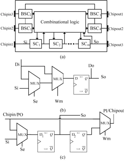
The DFT scan architecture with both boundary scan chain and regular scan chain is illustrated in Fig 1. The regular scan cell is modified from inherent flip flop in original design by introducing two 2-to-1 multiplexers. The shift output (So) of a scan cell is connected to the shift input (Si) of the next scan cell. Di and Do are the original data input and data output respectively. During the normal mode, both the work mode signal (Wm) and the scan-enable signal (Se) are set to 0. The packaged chip input pins (chipin) directly drive the primary inputs (PIs) of the circuit, while the primary outputs (POs) drive the chip output pins (chipout). That is, the boundary scan cells are transparent. The regular scan cells are determined by combinational logic. In the test mode, where Wm signal is set to 1, the boundary scan cells change the connection between the circuit input/outputs and chip pins. There are two phases in test mode. In the shift phase, where Se signal is set to 1, the test stimulus is shifted into two kinds of scan chains through the chip input pins and the test response is scanned out through the chip output pins. In capture phase, where Se signal is set to 0, the boundary scan cells drive the PIs and capture the states of POs while the regular scan cells capture the response of the combinational
Fig. 1. DFT scan architecture. (a) Overall DFT architecture with both boundary scan chain and regular scan chain. (b) Structure of regular scan cell
[image:2.595.47.287.447.759.2] [image:2.595.308.544.559.767.2]logic. The primary input/outputs of circuit can not be directly accessible in test mode.
B. AES
The AES is a round-based cipher algorithm with 128-bit block size. The key lengths could be 128, 192, and 256 bits. The number of rounds relies on the key-lengths. There are 10, 12, and 14 rounds for 128-bit key, 192-bit key, and 256-bit key, respectively. In the AES encryption, the input block is called plaintext and the returned ultimate output block is called ciphertext. The intermediate result block is called state. Except for the last round, each round consists of four basic transformations: SubBytes, ShiftRows, MixColumns and AddRoundKey. The last round does not contain MixColumns.
In the SubBytes transformation a nonlinear substitution operation is performed on each input bytes by use of a substitution function (called S-Box). In the ShiftRows transformation, each row of the input state is rotated to the left by a given number of bytes, which are related to the row number. The MixColumns transformation is the four-byte mixing operation in each column of the input state. In the AddRoundKey transformation the 128-bit input state is XORed with a 128-bit round key. The more details on the AES and its hardware implementations can be referred to [1].
III. PROPOSEDSECURESCANDESIGNS
Scan attack is powerful because intermediate result of just one round encryption can be accessed through shift operation and analyzed. The analyzing based on the one round encryption result and one or two round keys greatly decreases the difficulty of retrieving the secret key. The design objective for the secure scan-based DFT architecture should include:
1)Crypto module can be tested and debugged easily by
use of scan-based DFT.
2)Secret information stored in scan chains cannot be achieved to retrieve the secret key.
3)The information that can be obtained from scan chains should be irrelevant to the secret key.
A. Secure Scan Test Methodology
Based on the design goal above, we propose a secure scan test methodology, that protects the crypto chip against scan attack by simply modifying the conventional scan test methodology. To guarantee high test capability the proposed secure scan test methodology allows the key register to be configured as a scan chain (called key scan chain).
[image:3.595.307.549.350.739.2]The corresponding state jumping diagram of secure scan test is shown in Fig.2. A work mode select signal (Wm) is used to switch the chip under test between the normal and test mode. When Wm is set to 0, the chip is running in the normal mode, where the cryptographic operation is launched. When Wm becomes 0 from 1, the chip is first reset, i.e., scan chains in it are reset. The secret information will be erased by this way. Then it is running in the test mode. The test mode includes two phases of operations: shift operation and capture operation. The scan-enable signal (Se) is used to switch the chip between the two phases of operations. In the
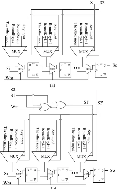
Fig. 3. Scan chain with system reset. (a) the structure of conventional DFT scan chain with system reset. (b) the structure of proposed secure DFT scan chain with reset operation.
(b) Wm (a) So Q Q SET CLR D Key inp ut Round Key i-1 T he ot he r in pu t MUX Roun dKey i+ 1 Q Q SET CLR D Key inp ut Round Key i-1 T
he other input
MUX Roun dKeyi+1 Q Q SET CLR D Key input Ro undKeyi-1 T he ot he r in pu t MUX Ro undKeyi+1 Si S1 S2 Wm So Q Q SET CLR D Key inp ut Roun dKey i-1 T he o the r i npu t MUX Roun dKey i+ 1 Q Q SET CLR D Key inp ut Roun dKeyi-1 T
he other input
MUX Rou ndKeyi+1 Q Q SET CLR D Key input Ro undKeyi-1 T he o the r i npu t MUX Round Keyi+ 1 Si S1 S2 Wm
MUX MUX MUX
MUX MUX MUX
[image:3.595.47.280.487.752.2]S2' S1'
shift phase, where Wm=1 and Se=1, a test pattern is shifted serially into the scan chains through the chip input pins. Once the holonomic test pattern is fed into the scan chains, Se is set to 0 to switch the chip to capture phase for one clock cycle. In capture phase, the response from combinational logic will be captured into the scan cells.
It’s possible that the hacker misuses the capture operation to load the key into key scan chain. Therefore, loading key in capture operation will be prohibited in the propose scheme. By setting Se to ‘1’ again, the captured response is shifted out of scan chains through the chip output pin while the next test pattern is scanned into the scan chains.The work modes of the chip can be switched freely. Once the mode switching is requested, the chip is immediately reset.
B. Secure Scan Test Architecture
In the proposed secure scan test methodology, there are two distinctive features, i.e. the scan chain reset mechanism and keeping secret key isolated from key scan chains in the test mode. In view of these points we develop a secure scan test architecture. The architecture consists of two parts: scan chain structure with reset operation and the data input architecture of key scan chain, which are illustrated in Fig.3(b) and Fig.4(b), respectively.
In conventional scan design, the system reset signal (System_Reset) controls directly the reset input (CLR) of each flip flop and is used to initialize the system, as illustrated in Fig. 3(a). To implement the reset operation in case of mode switching in a low area overhead way, we introduce a D flip flop, a XOR gate and a OR gate for the system reset signal, as shown in Fig. 3(b). The added flip flop stores the previous Wm. The XOR gate combines the previous Wm and the current Wm by using the Boolean XOR operator. The reset control signal of each flip flop is System_Reset ORed with the output of the XOR gate. Suppose that, the reset operation is valid when CLR signal of the flip flop is high. When Wm changes (from 0 to 1 or from 1 to 0), the output of the XOR gate will be ‘1’ and the output of OR gate will also be ‘1’ regardless of the system reset signal. Just then the states of all the flip flops are cleared to protect secret information.
It is also important to note that the reset operation can be performed normally when System_Reset is ‘1’.
The proposed secure scan test architecture is implemented on an AES chip. The key unit, which is utilized to store keys and to calculate the key expansion function, is an important part of AES hardware implementation[1]. In the original design, each storage element (flip flop) of key unit receives four input signal through a multiplex: secret key input, the next round key input (Roundkeyi+1), the previous round key
used for decryption (Roundkeyi-1) and the other input, as
illustrated in Fig .4 (a). Each multiplex has 2-bit control signals (marked as S1 and S2 in the figure) which select one input from four. The secret key is typically stored in non volatile memory. When the chip is power on and {WmS1S2}={000}, the secret key is loaded into key register. The round keys are generated based the secret key. If the secret key is allowed to load into key register in test mode, the crypto chip takes great risk as it opens a back door to leak secret information. Because of this, in the propose secure scan test methodology, we prohibit the key load during the
capture operation of test mode. Note that each key scan cell receive data from its predecessor through Si input during shift operation, and it’s impossible to leak secret.
One can disable each key input by adding a three state NOT gate. However, it needs a little large area overhead. To reduce the extra overhead, we disable the key input in the capture phase by revising the control signals of the multiplex as indicated in Fig. 4(b). Wm is utilized to help control the multiplex through two logic gates (a NOR gate and a OR gate). S2 is maintained constant by comparison with that in Fig. 4(a).When the chip works in normal mode (Wm=0), these logic gates are transparent. When Wm=1, the case that {S1'S2'}={00} can never come into existence even if {S1S2}={00}. That is, loading key into register will be always forbidden in test mode. The relation between {S1'S2'} and {WmS1S2} is described in table 1.
TABLEI
THE RELATION BETWEEN {S1'S2'} AND {WmS1S2}
Wm S1S2 S1'S2'
0 00 00
0 01 01
0 10 10
0 11 11
1 00 10
1 01 01
1 10 10
1 11 11
IV. PERFORMANCEANALYSIS
A. Testability Analysis
The proposed secure design does not hurt the controllability and observability of chip under test at all. The test patterns can be loaded into scan chains just like the original scan design. Consequently, the testability of original scan design is not affected and fabrication testing and in-field debugging can be launched normally.
In many techniques the key register does not join in scan chains for the sake of security. However,in our proposed scheme the key register are configured as key scan chain and thus higher fault coverage could be achieved as more test patters can be applied.
When the chip works in the functional mode, extra logic structure in the secure scan design is transparent and the performance of chip is hence not compromised.
B. Security Analysis
Whatever method the scan based attacks utilize, the intermediate result gained from scan chain are essential. However, all the information in scan chains are always cleaned once the mode switching happens. The mode-switching attacks can thereby be overcome.
Besides, the secret information never exist in scan chains under test mode since loading key into register is always forbidden at these cycles. The round keys Roundkeyi+1 and
Roundkeyi-1 could be loaded into key scan chain.
C. Area Overhead Analysis
Compared with the conventional scan architecture, the proposed secure scan architecture needs merely three logic gates and one D flip flop. The extra overhead is not dependent on the scale of circuits and the length/number of scan chains. We could reasonably argue that the area overhead of the proposed secure scan architecture is completely negligible.
V. CONCLUSION
The scan-based DFT design imposes a great potential threat to the security of cryptographic chip while enhancing the test quality of IC. To defeat the scan-based attacks without compromising the testability of chips, we proposed a secure scan test countermeasure to protect the crypto chips. The proposed secure design provides the scan chain reset mechanism and isolates the secret key from scan chains during test mode, thereby overcoming all known scan attacks. The area overhead of the proposed secure scan countermeasure is extremely low and can be completely ignored. This is the greatest advantage of the proposed technique.
REFERENCES
[1] S. Mangard, M. Aigner, and S. Dominikus, “A highly regular and scalable AES hardware architecture,” IEEE Trans. Comput., vol. 52, no. 1, pp. 483-491, Apr. 2004.
[2] D. Xiang, Y. Zhao, K. Chakrabarty, et a1, “A Reconfigurable Scan Architecture With Weighted Scan-Enable Signals for Deterministic BIST,”. IEEE Trans. Computer Aided Design of Integrated Circuits
and Systems, vol. 27, no. 6, pp. 999-1012, June 2008.
[3] L.-T. Wang, C.-W. Wu, and X. Wen, VLSI Test Principles and
Architectures. San Mateo, CA:Morgan Kaufmann, 2006.
[4] F. Koeune, F-X. Standaert, “A tutorial on physical security and sidechannel attacks,” Foundations of Security Analysis and Design III. Springer Berlin Heidelberg. 2005, pp. 78-108.
[5] B. Yang, K. Wu, and R. Karri, “Scan based side channel attack on dedicated hardware implementations of data encryption standard,” in
Proc. International Test Conference, Charlotte, 2004, pp. 339-344.
[6] R. Nara, N. Togawa, M. Yanagisawa, and T. Ohtsuki, “Scan-based attack against elliptic curve cryptosystems,” in Proc. Asia and South
Pacific Des. Autom. Conf., Taipei, Taiwan, Jan. 2010, pp. 407- 412.
[7] R. Nara, K. Satoh, M. Yanagisawa, and N. Togawa, “Scan-based sidechannel attack against RSA cryptosystems using scan signatures,”
IEICE Trans. Fundamentals Electron., Comm. Comput. Sci., vol.
E93-A, no. 12, Dec. 2010, pp. 2481-2489.
[8] J. Da Rolt, G. Di Natale, M. Flottes, and B. Rouzeyre, “A novel differential scan attack on advanced DFT structures,” ACM
Transactions on Design Automation of Electronic Systems, vol. 18, no.
4, article no. 58, Oct. 2013.
[9] D. Hely, F. Bancel, M.-L. Flottes, and B. Rouzeyre, “Test control for secure scan designs,” in Proc. European Test Symp., Tallinn, Estonia, May 2005, pp. 190-195.
[10] S. S. Ali, O. Sinanoglu, S. M. Saeed, and R. Karri, “New scan attacks against state-of-the-art countermeasures and DFT,” in Proc. IEEE Int.
Workshop Hardware-Oriented Security Trust, Arlington, VA, USA,
May 2014, pp. 142-147.
[11] S. S. Ali, O. Sinanoglu, R. Karri, “Test-mode-only scan attack using the boundary scan chain,” in Proc. European Test Symp., Paderborn, Germany, May 2014, pp. 1-6.
[12] S. S. Ali, S. M. Saeed, O. Sinanoglu, and R. Karri, “Novel test-mode only scan attack and countermeasure for compression-based scan architectures,” IEEE Transactions on Computer-Aided Design of
Integrated Circuits and Systems, vol. 34, no. 4, pp. 808-821, May 2015.
[13] Y. Bo, W. Kaijie, and R. Karri, “Secure scan: A design-for-test architecture for crypto chips,” IEEE Transactions on Computer-Aided
Design of Integrated Circuits and Systems, vol. 25, no. 10, pp.
2287-2293, Oct. 2006.
[14] J. Lee, M. Tehranipoor, C. Patel, and J. Plusquellic, “Securing designs against scan-based side-channel attacks,” IEEE Trans. Dependable
Secure Computing, vol. 4, no. 4, Oct. 2007, pp. 325-336.
[15] Y. Atobe, Y. Shi, M. Yanagisawa, and N. Togawa, “Secure scan design with dynamically configurable connection,” in Proc. 19th IEEE
Pacific Rim Int. Symp. Dependable Computing (PRDC), Vancouver,
Canada, Dec. 2013, pp. 256-262.
[16] H. Kodera, M. Yanagisawa, and N. Togawa, “Scan-based attack against DES cryptosystems using scan signatures,” in Proc. Asia
Pacific Conf. Cir. Syst. (APCCAS), Kaohsiung, Taiwan, Dec. 2012, pp.
2-5.
[17] R. Nara, N. Togawa, M. Yanagisawa, and T. Ohtsuki, “A scan-based attack based on discriminators for AES cryptosystems,” IEICE Trans.
Fundamentals Electron., Comm. Comput. Sci., vol. E92-A, no. 12,
Dec. 2009, pp. 3229-3237.
[18] O. Novák; J. Jeníček; M. Rozkovec, “Sequential test decompressors with fast variable wide spreading,” 2016 IEEE 19th International Symposium on Design and Diagnostics of Electronic Circuits &
Systems, Kosice, Slovakia, April 2016, pp. 132-137.
[19] J.-H. Kang, N. A. Touba, J.-S. Yang, “Reducing control bit overhead for X-masking/X-canceling hybrid architecture via pattern partitioning,” in Proc. 53nd ACM/EDAC/IEEE Design Automation
Conference, Jun 2016, Austin, USA, pp. 344-349.
[20] A. Das, B. Ege, S. Ghosh, L. Batina, and I. Verbauwhede, “Security analysis of industrial test compression schemes,” IEEE Trans. CAD of Integr. Cir. Syst., vol. 32, no. 12, Dec. 2013, pp. 1966-1977. [21] IEEE Standard Test Access Port and Boundary Scan Architecture,
IEEE Standard 1149.1-2001, Jul. 2001, pp. 1-212.
[22] J. D. Rolt, A. Das, G. D. Natale, M. -L. Flottes, B. Rouzeyre, and I. Verbauwhede, “Test Versus Security Past and Present,” IEEE Trans.
On Emerging Topics in Computing, vol. 2, Feb. 2014, pp. 50-62.
[23] Y. Luo, A. Cui , G. Qu, et al. “A new countermeasure against scan-based side-channel attacks,” in Proc. IEEE International