New Modulation Scheme for Bidirectional quasi Z-Source Modular
Multilevel Converters
Fatma A. Khera
*
,†Christian Klumpner
*
Pat W Wheeler
*
*
Power Electronics, Machines and Control Research Group, University of Nottingham, Nottingham, UK †Electrical Power and Machines Engineering Department, Tanta University, Egypt E-mail: [email protected], [email protected]
Keywords: quasi Z-source, modular multilevel converter.
Abstract
This paper proposes a dedicated modulation scheme for a bidirectional quasi Z-source modular multilevel converter (BqZS-MMC). The operation principle and a suitable PWM method are proposed. The relation between the modulation index and shoot-through duty ratio is derived. A formula for calculating the required value of quasi Z-source capacitance is given. The simulation results presented in the paper validate the operation and the performance of the proposed topology.
1 Introduction
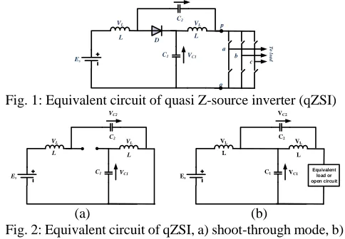
Multilevel inverters (MLIs) are preferred due to their attractive features compared to two-level voltage source inverters (VSIs) [1] such as better AC voltage quality, low voltage stress on semiconductors, possibility to produce significantly higher voltages than a single switch voltage rating. The modular multilevel converter (MMC) is a relatively new competitive concept which has been proposed in 2002 [2]. It provides several features such as modularity, voltage and power scalability and failure management capability in the case of device failures [3]. These advantages favour the MMC for various applications, such as interface to high voltage direct current (HVDC) [4] and flexible AC transmission (FACTs) systems[5], medium-voltage (MV) motor drives applications [3] and connecting renewable energy sources such as photovoltaics [6] and wind energy system [7] to MV grids. The output voltage of most renewable energy sources fluctuates with working conditions, therefore having a converter that can adapt to these fluctuation by being able not only to step down but also to step up the voltage in order to regulate the voltage at the DC-link terminals may be quite useful. Power converter topologies based on the use of impedance network concept have been proposed in [8] which proposes the implementation of a quasi Z-source modular multilevel converter. The basic structure of the quasi Z-source inverter (qZSI) as proposed in [9] is shown in Fig. 1. The operating principle of the qZS network relies on producing a short circuit (shoot-through) at inverter DC-link terminals in order to increase the stored energy in the inductors that is later transferred in the qZS capacitors and finally, this extra voltage adds up to the DC source voltage and provides voltage boosting capability. There are two operation modes for qZS-network which are shoot-through (ST) and non-shoot-through mode (NST). In ST mode, the DC-link terminals are shorted by gating both the upper and lower devices of at least one inverter leg, which forces the
qZS diode D to become reverse biased and therefore behave like an open circuit as shown in Fig. 2a. Hence, the stored energy in the capacitors begins to transfer into the inductors. In NST mode, the inverter operates by producing active and null voltage states [11] and then D will be forward biased as shown in Fig. 2b, the stored energy in the inductors begins to transfer to the load, which sees Vpo=Vc1+Vc2 as its DC-link voltage, and qZS
capacitors begin to charge.
VL
D
Es
T
o
load
L C2
VL
a b
c VC2
VC1
C1
p
[image:1.612.321.563.267.435.2]o L
Fig. 1: Equivalent circuit of quasi Z-source inverter (qZSI)
VL
Es
L C2
VL
VC2
VC1
C1
L
(a)
VL
Es
L C2
VL
VC2
VC1
C1 Equivalent load or
open circuit
L
(b)
Fig. 2: Equivalent circuit of qZSI, a) shoot-through mode, b) non shoot-through mode
Ref [8] proposed the integration of qZS-network with a single phase MMC to provide voltage boost capability. The proposed circuit faces some limitations which were identified in the same paper and a solution was proposed by modifying the qZS-MMC to be a bidirectional one (BqZS-MMC).
This paper gives a detailed circuit analysis of the proposed BqZS-MMC. The equivalent circuit of the qZS-MMC with the proper implemented sinusoidal pulse width modulation (SPWM) boosting scheme is presented which can be extended to any number of output voltage levels. The relation between modulation index and shoot-through duty ratio for any number of voltage levels is derived. A guideline for choosing the value of qZS capacitance is proposed. Finally, the operation and analysis of the proposed modulation scheme is validated using results simulation from a MATLAB/PLECS model.
2 Operation principles of the bidirectional quasi
Z-Source modular multilevel converter
with one DC-link capacitor. The two switches (Sa, and Sax) in
SM are controlled by complementary gating signals. When Sa is
on, SM capacitor is bypassed and SM terminal voltage is zero. If Sa is off, Sax is on, therefore SM terminals voltage is Vc and
SM capacitor is inserted into the circuit. Each sub-module capacitor needs to be charged by a fraction of DC bus voltage
E/N where N is the number of sub-modules per arm. Therefore, the output voltage (Vao) swings between –Vpn/2 and Vpn/ and
each arm should aim to produce the reference output voltage potential, as average over one switching period. Output inductors Lo have the role to limit the current ripple caused by
the momentary mismatch of voltage produced by the two arms, and also enable the control of circulating current needed to replenish the energy in the SM capacitors. The modulation scheme for generating these states will be explained in § IV.
[image:2.612.49.277.242.434.2]E is p n o vcu1 vcn2 vcn1 vcu2
i
Lu2i
Lu1i
Ln2i
Ln1i
cn1 Su Sn L o w er a rm -a U p p er a rm -a Lo Lo a SM1 SM2 SMN Cu1 Cn1 Cn2 Cu2 Sa Sax Vc vpo von vpa van Vao Du Tu Dn Tni
ani
paFig. 3: Typical topology of an N-cell single-phase MMC The output voltage equation as a function of the upper arm, lower arm and the DC-link voltages are given by:
2 2 on po pa an ao v v v v v
(1)
From (1), if the upper qZS-network is shorted via Su, i.e. vpo=0,
the upper arm voltage vpa should be reduced to keep the required output voltage at certain level which can be achieved by reducing the number of inserted cells in the upper arm by N/2. The same procedure is followed if the lower qZS-network is shorted via Sn. In this study, phase disposition SPWM
(PD-SPWM) is used to control the MMC arms [10]. The Su and Sn
have been modulated using the proposed technique as follows.
3 MMC capacitors voltage balancing and
modulation scheme
3.1 Capacitor voltage balance
The MMC requires a voltage balancing strategy to balance and keep the sub-modules capacitor voltages at their desired average values. The implementation of balancing strategies depends on the presence of the redundant states in the MMC arm [11]. The redundant switching state with the strongest effect in
facilitating voltage balancing is always selected. The MMC arm capacitors balancing can be achieved by different strategies [11]. The most widely used balancing strategy is based on the sorting method [6] which is summarized in four steps as follows: 1) Measure and sort the upper and lower capacitor voltages; 2) From modulation scheme, determine the number of inserted
cells (np and nn) from upper and lower arms respectively;
3) If the upper (lower) arm current is positive where current direction shown in Fig. 3 is considered as positive, choose the np (nn) cells with lower voltage to be inserted. Therefore,
the corresponding cell capacitor is charged and its voltage increases;
4) If the upper (lower) arm current is negative, choose the np
(nn) cell with higher voltage to be inserted. Therefore, the
corresponding cell capacitor is discharged and its voltage decreases.
3.2 Modulation scheme
To synthesize n-level voltage waveform at the converter AC-side where n equal 2N-1, phase disposition SPWM (PD-SPWM) with two complementary reference signals (vmn and
vmu) is used in this study to control the BqZS-MMC as indicated
in Fig. 4. Each carrier is responsible for producing the gating signals of two cells (one from upper and one from lower arm). The reference signals are compared against the carriers to define which leg-switches are conducting. The upper (lower) qZS-networks can be in shoot-through (ST) mode if the number of upper (lower) inserted cells equals or is higher than N/2. Therefore, the number of inserted cells can be reduced by N/2 to obtain the required voltage level. According to this concept, this modulation scheme can be named as reduced number of the inserted cell (RNIC) technique. By considering N =4, the number of output voltage level will be nine as clarified in Fig. 4. Table 1 lists the available voltage levels when N=4 by clarifying the number of inserted SMs in both upper and lower arms for each level before and after introducing ST intervals and which qZS-network switches Su and Sn should be gated. Su can
be shorted during all output voltage levels except levels 1, 2 and 3 (7, 8 and 9 for Sn) as shown in Table 1 and Fig. 4, because at
these levels, the number of inserted cells from the upper (lower) arm is less than two (N/2). Therefore, ST signals of Su at levels
1, 2 and 3 are set to zero.
Fig. 4 shows the output voltage waveform, ST signals and the gating signals for both Su and Sn. The upper ST signal (Vsh-u) is
defined by:
2 2
2 1 1 2
_
1 1
0 ; 2
/ 2 s i n ;
1
1 2
s h s h s h u
s h
M t t
N M w t t t
V t M t (2)
Where Msh is the ST modulating signal height as shown in Fig.
4. In the range from ϴ1 to π- ϴ1, the number of inserted SMs per arm became lower than N/2, where shoot-through interval should set at zero, ϴ1is defined by:
) / 2
( sh
-1
1 sin NM
The lower ST signal Vsh-n waveform is the same shape as Vsh-u
but shifted by 180oas shown in Fig. 4. The pulses of S
u and Sn
are generated if carrier signal Csh is higher than Vsh-u and Vsh-n
respectively. According to Vsh-uand Vsh-n signals, the output
voltage reference waveforms (Vmu and Vmn) for the upper and
lower arms are modified as shown in Fig. 5 in order to provide a reduction in the number of inserted cells during these intervals by two cells (N/2). From (2), the instantaneous value of duty ratio is given by:
s h 2 2
s h _ u s h 2 1 1 2
1 1
1 -M 0 < ω t< θ ;π -θ < ω t< 2 π
d = 1 -N /2 × M s in w t θ < ω t< θ ;π -θ < ω t< π -θ
0 θ < ω t< π -θ
(4)
By integrating (4), the average shoot-through duty ratio Dsh can
be calculated which is given by:
s h 2 s h 1 2
D = ( π + 2 θ )(1 -M )/2 π + (θ -θ )/π
s h 1 2
+ N M ( c o s θ - c o s θ ) /π (5)
From (5), The DC-link voltage can be expressed by:
E ) 2D -1/(1
Vpn sh
E
N
M sh(2 (cos cos ) 2 )
21 1 2 2
[image:3.612.322.563.76.345.2] (6)
Fig. 5 shows the normalized peak DC-link voltage versus shoot-through duty ratio Msh when N=2, 4, 6, 8 and 10. By increasing
the number of sub-modules, higher Msh is required at the same
DC link voltage. The qZS-capacitors voltages are given by:
2 / ) pn
sh cn1
cu1 V (1 D V
V ;
2 /
pn sh cn2
cu2 V D V
V (7)
For N of SMs per arms, the SMs capacitor voltages are given by:
Vca r m Vp n / N
(8)
From (8), the peak value of the fundamental output voltage is given by:Vm MNV carm /2 GE /2 (9)
Level number
Voltage level
Number of SMs inserted
N=4 (Upper, Lower) (Su, Sn)
before after
1 - Vpn /2 4, 0 2, 0 (1, 0)
2 -3 Vpn /8
4, 1 3, 0
2, 1
1, 0 (1, 0)
3 - Vpn /4 3, 1 1, 1 (1, 0)
4 - Vpn /8 3, 2
2, 1
3, 0 0, 1
(0, 1) (1, 0)
5 0 2, 2 0, 2
2, 0
(1, 0) (0, 1)
6 Vpn /8 1, 2
2, 3
1, 0 0, 3
(0, 1) (1, 0)
7 Vpn /4 1, 3 1, 1 (0, 1)
8 3 Vpn /8 1, 4
0, 3
1, 2
0, 1 (0, 1)
[image:3.612.44.295.121.330.2]9 Vpn /2 0, 4 0, 2 (0, 1)
Table 1: The available voltage levels with clarifying the number of inserted SMs in both upper and lower arms
Where G is given as a function of Dsh (or Msh) and output voltage
modulation index M by:
1 1
3 / [ ( 4 6 3 1 2 c o s ) 6 ]
s h
s h
G M / ( 1 - 2 D )
M M
(10)
1 2 3
4 5 6
7 8
9
O
u
tp
u
t
vo
lt
a
ge
w
av
ef
o
rm
s
Sh
o
o
t-th
ro
u
gh
m
o
d
u
la
ti
o
n
s
ign
a
ls
Su
Sn
Msh
ϴ2ϴ1 Π-ϴ1 Π-ϴ2
ωt
Fig. 4: The PD-PWM with double reference waveforms, the shoot-through modulation signals and the generated pulses for RNIC technique.
Fig. 5: The modified output voltage reference waveforms according to the shoot-through pulses for RNIC technique.
Fig. 6: Normalized DC-link voltage Vpn/E, versus shoot through
[image:3.612.332.541.398.513.2] [image:3.612.42.294.484.697.2] [image:3.612.335.530.549.689.2]4 Choosing values of passive element
According to [8], using an IGBT in antiparallel to the diode D in the BqZS-network allows the converter to operate with small values of inductance without disturbing the operation of the circuit, being able to completely avoid the undesirable operation modes found in [8], consequently, eliminating any drops in the dc-link voltages that affected the output harmonic distortion. However, the qZS inductance value should be chosen for limiting the ripples to a reasonable level (20%) to reduce the current stress on the converter devices.
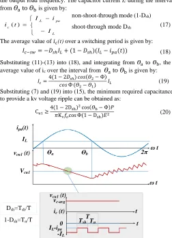
The inductance value of the four inductors is chosen according to [12]. The arm inductance and SM capacitance are calculated according to the relevant study and the relations given in [13]. In this section, the general relation for determining the proper qZS-capacitance value has been obtained. According to [8], the qZS-capacitor voltages Vcu1 and Vcu2 (Vcn1 and Vcn2) decrease
when the arm current value ipa(ina) is higher than average value
of inductor current IL during both ST and NST modes as
indicated in Fig. 7. The interval when the arm current is higher than the average inductor current ranges between 𝛳a and 𝛳b where 𝛳a and 𝛳b are the two instants when the arm current is equal to IL. The upper and lower arm currents can be expressed by:
dc 2f a
pa i /2 i I
i ; ina ia/2 i2f Idc (11)
where Idc is the DC component in arm currents which is
responsible for transferring real active power from the supply to the load. The, i2f is the second order harmonic usually present
in any single phase converters and ia is the AC load current
component. In the following analysis, the value of the 2nd order
harmonic is not a significant as ia, so i2f is not considered and
set to zero in (11). From power balance equation, the maximum value of the load current Iacan be calculated by:
Ia=
2𝐸IL
Vm𝑐𝑜𝑠Фsin (𝜔𝑡 − Ф) (12)
Where Ф is the load displacement angle, Idc s the
DC-component in the arm current which can be calculated as a function of the average value of qZS-inductor current by:
Idc=1 − 2D1 − Dsh
sh IL (13)
Substituting by (12) and (13) into (11), and equating the resultant equation by IL, 𝛳a and 𝛳b can be calculated by:
𝛳a = sin−1(2(1 − 2𝐷𝐷𝑠ℎ
𝑠ℎ)𝑐𝑜𝑠Ф) + Ф
𝛳b = 𝜋 − sin−1(2(1 − 2𝐷𝐷𝑠ℎ
𝑠ℎ)𝑐𝑜𝑠Ф) + Ф
(14)
The capacitance Cu1can be obtained by:
𝐶𝑢1=𝛥𝑣𝐼𝑐𝛥𝑡
𝐶𝑢1 (15)
According to Fig. 7, Δt and ∆vcu1can be defined as:
∆𝑣𝑐𝑢1= 𝑘𝑣𝑉𝑐𝑢1 & 𝛥𝑡 =𝛳𝑏2𝜋− 𝛳𝑎∗𝑓1
𝑜 (16)
Where Vcu1 is the average value of the qZS capacitor voltage kv, is the
ratio between peak to peak capacitor voltage ∆𝑣𝑐𝑢1and 𝑉𝑐𝑢1 and 𝑓𝑜 is
the output load frequency. The capacitor current Ic during the interval
from 𝛳a to 𝛳bis given by:
L pa L
c
I i I t i ( )
non-shoot-through mode (1-Dsh)
(17) shoot-through mode Dsh
The average value of 𝑖𝑐(t) over a switching period is given by:
𝐼𝑐−𝑠𝑤= −𝐷𝑠ℎ𝐼𝐿+ (1 − 𝐷𝑠ℎ)(𝐼𝐿− 𝑖𝑝𝑎(𝑡)) (18)
Substituting (11)-(13) into (18), and integrating from 𝛳a to 𝛳b, the average value of ic over the interval from 𝛳a to 𝛳b is given by:
𝐼𝑐=
4(1 − 2𝐷𝑠ℎ) 𝑐𝑜𝑠(𝛳2− Ф)
𝑐𝑜𝑠 Ф (𝛳2− 𝛳1) 𝐼𝐿 (19)
Substituting (7) and (19) into (15), the minimum required capacitance to provide a kv voltage ripple can be obtained as:
Cu1≥
4(1 − 2Dsh)2cos(𝛳b− Ф)𝑃
𝜋Kv𝑓𝑜cos Ф(1 − Dsh)𝐸2 (20)
IL
ipa(t)
ω t
ϴa ϴb
vcu1 (t)
Vcu1
ω t 2π
0
-IL
IL-ipa
T Tsh Tn
ic (t)
vc-avg
t
t
Dsh=Tsh/T
1-Dsh=Tn/T
vcu1 (t)
Fig. 7: a) The upper arm current, the qZS capacitor voltage waveform, the zooming of capacitor voltage and currnt waveform
5 Simulation results
To verify the validity of the proposed modulation scheme for the BqZS-MMC, a simulation model is implemented in MATLAB/PLECS for the proposed configuration shown in Fig. 2 with a number of SMs equal to 6. The parameters used in the simulation models are given in Table 2. The simulation study has been carried out using a passive (R+L) load and considering that all system components and switches are ideal.
The optimum qZS-capacitors (Cu1 and Cn1) were calculated in
order to provide the voltage ripple factor kv of about 10%. Based
on the parameters in Table 2, the required value of the qZS-capacitor is around 3.15 mF which is calculated by (20).
The converter modulation index M is set at 1 and the shoot-through modulation index Msh is set to 0.8 (boost), 0.6 (boost)
and 1 (buck) and consequently the shoot-through duty ratio Dsh
is equal 0.124, 0.256 and zero respectively.Fig. 8 and Fig. 9 shows the upper, lower and overall DC link voltage, and their zooming respectively. By lowering Msh from 0.8 to 0.6, the peak
value of overall DC-link voltage is increased from 4kV to 6.2kV. Also, to check the operation in buck mode, Msh is set at 1, where
[image:4.612.314.566.59.407.2]The simulation results of qZS-network capacitor (Vcu1, Vcn1, Vcu2
and Vcn2)and arm capacitor voltages are shown in Fig. 10 and
Fig. 11 illustrates their zooming. These capacitors are charged according to the relations given in (7) and (8). The ripple factor
kvof Vcu1 and Vcn1 is around to 10% which confirm the validity of
the proposed capacitance formula. Load voltage and current are shown in Fig 12. For the proposed BqZS-MMC, by lowering
Msh from 0.8 to 0.6, the peak value of output voltage fundamental
component is increased from 2kV to 3.1kV. However, for traditional MMC, the peak value of the output voltage is limited to half value of supply voltage (E/2=1500V). The output current shown in Fig. 12 does not show low order harmonics, which is a sign that the proposed modulation works as expected.
Source voltage E 3kV Load inductance
and resistance 14 mH, 13 Ω
qZS-networks
inductances 10 mH
qZS-networks
Capacitances 3.3 mF
MMC-arm
inductance 5mH
MMC-arm
capacitances 3.3 mF
Switching
frequency 2 kHz Output frequency fo 50 Hz
Table 2: ZSI simulation model parameters
6 Conclusion
This paper proposed a modulation scheme for bidirectional quasi Z-source modular multilevel converter topology that is able to achieve buck and boost voltage capabilities. The relation between modulation index and average shoot-through duty ratio has been derived and verified by simulation at different modulation indexes in both buck and boost mode. An analytical design methodology for calculating the required values of quasi Z-source capacitors has been proposed and the resulting ripples in the simulation match the ripple imposed in the design.
References
[1] H. Abu-Rub, J. Holtz, J. Rodriguez, and G. Baoming, "Medium-Voltage Multilevel Converters-State of the Art, Challenges, and Requirements in Industrial Applications," IEEE Transactions on Industrial Electronics, vol. 57, pp. 2581-2596, 2010.
[2] A. Lesnicar and R. Marquardt, "An innovative modular multilevel converter topology suitable for a wide power range,"
in 2003 IEEE Bologna Power Tech Conference Proceedings, 2003, p. 6 pp. Vol.3.
[3] S. Debnath, J. Qin, B. Bahrani, M. Saeedifard, and P. Barbosa, "Operation, Control, and Applications of the Modular Multilevel Converter: A Review," IEEE Transactions on Power Electronics, vol. 30, pp. 37-53, 2015.
[4] M. Saeedifard and R. Iravani, "Dynamic performance of a modular multilevel back-to-back HVDC system," in 2011 IEEE Power and Energy Society General Meeting, 2011, pp. 1-1. [5] A. U. Lawan, H. Abbas, J. G. Khor, and A. A. Karim, "Dynamic
performance improvement of MMC inverter with STATCOM capability interfacing PMSG wind turbines with grid," in 2015 IEEE Conference on Energy Conversion (CENCON), 2015, pp. 492-497.
[6] R. Guruambeth and R. Ramabadran, "Fuzzy logic controller for partial shaded photovoltaic array fed modular multilevel converter," IET Power Electronics, vol. 9, pp. 1694-1702, 2016. [7] T. Nakanishi, K. Orikawa, and J. i. Itoh, "Modular Multilevel Converter for wind power generation system connected to micro-grid," in 2014 International Conference on Renewable Energy Research and Application (ICRERA), 2014, pp. 653-658. [8] F. A. Khera, C. Klumpner, and P. W. Wheeler, "Operation
Principles of Quasi Z-Source Modular Multilevel Converters", in 2017 IEEE 3nd Annual Southern Power Electronics Conference (SPEC), 2017.
[9] J. Anderson and F. Z. Peng, "A Class of Quasi-Z-Source Inverters," in 2008 IEEE Industry Applications Society Annual Meeting, 2008, pp. 1-7.
[10] X. Shi, Z. Wang, L. M. Tolbert, and F. Wang, "A comparison of phase disposition and phase shift PWM strategies for modular multilevel converters," in 2013 IEEE Energy Conversion Congress and Exposition, 2013, pp. 4089-4096.
[11] G. P. Adam, O. Anaya-Lara, G. M. Burt, D. Telford, B. W. Williams, and J. R. Mcdonald, "Modular multilevel inverter: Pulse width modulation and capacitor balancing technique," IET Power Electronics, vol. 3, pp. 702-715, 2010.
[12] S. Rajakaruna and L. Jayawickrama, "Steady-State Analysis and Designing Impedance Network of Z-Source Inverters," IEEE Transactions on Industrial Electronics, vol. 57, pp. 2483-2491, 2010.
[image:5.612.53.525.513.701.2][13] M. Zygmanowski, B. Grzesik, and R. Nalepa, "Capacitance and inductance selection of the modular multilevel converter," in 2013 15th European Conference on Power Electronics and Applications (EPE), 2013, pp. 1-10.
Fig. 8: The upper, lower and and overall DC link voltage at Msh=0.8, 0.6 and 1 from left to right respectively.
Fig. 9: Zooming of the upper, lower and and overall DC link voltage at Msh=0.8, 0.6 and 1 from left to right respectively.
Fig. 10: The qZS-network capacitor and arm capacitor voltages at Msh=0.8, 0.6 and 1 from left to right respectively
Fig. 11: Zooming of the qZS-network capacitor and arm capacitor voltages at Msh=0.8, 0.6 and 1 from left to righrespectively
[image:6.612.67.533.214.526.2]