Design of Microstrip Patch Circular Slotted
Antenna using Microstrip Line Feed Technique
Harmandeep Kaur1, Er. Mandeep Kaur2
1
M.Tech, Scholar, Department of Electronic & Communication Engineering, Khalsa College of Engineering &Technology, Amritsar.
2
Assistant Professor, Department of Electronic & Communication Engineering, Khalsa College of Engineering & Technology, Amritsar.
Abstract: This paper takes research on design of multiband microstrip patch antenna. The proposed patch antenna can resonate at five unique frequencies between 2 GHz and 9GHz out of which five are considered to be useful bands. To accomplish multiband frequency, proposed finite element method is employed to design the rectangular Microstrip Patch Antenna (MPA). The rectangular shapes and a circular slot are etched from the patch to improve the gain of antenna. The proposed antenna is designed on FR4 Epoxy substrate with specifications: relative permittivity = 4.4, relative permeability = 1, di-electric loss tangent =0.02 and thickness = 1.6 mm .The return loss for all the resonant frequencies is less than -10dB. The proposed design exhibits the the gain of 3.9dB, 2.7dB and 9.74dB at 5.1GHz, 6.9GHz and 8.5GHz respectively, and can be used for wireless applications like wireless broadband transceiver which is applicable to mobile Wi max, fixed Wi max, RADAR applications including continuous wave pulsed, single polarisation, dual polarisation and air traffic control.
Keywords: MPA, feeding techniques, return loss and gain.
I. INTRODUCTION
Antennas enables wireless communication between two or more stations by directing signals from one station to another by radio waves [1]. A microstrip patch antenna (MPA) comprise of metallic patch radiator on an electrically thin di-electric substrate with the ground of metallic material such as copper, gold. Micro strip antenna consists of a very thin metallic strip placed on a ground plane with a di-electric material in-between. The radiating element and feed lines are placed by the process of photo-etching on the di-di-electric material. Usually, the patch or micro-strip is chosen to be square, circular or rectangular in shape for the ease of analysis and fabrication. The following image shows a micro-strip or patch antenna. The length of the metal patch is λ/2. When the antenna is excited, the waves generated within the di-electric undergo reflections and the energyis radiated from the edges of the metal patch, which is very low. To meet such features and requirements, the microstrip patch antenna have been proposed because of its low profile, less in cost, small in size.[1] Microstrip Patch Antenna consists of rectangular patch which is conductor in nature of length "L" and width "W" on one side of dielectric substrate with the thickness of "h" and dielectric constant "εr" with the base named ground. Common microstrip antenna shapes
which we use are circular , elliptical , square, rectangular, but any shape is possible like introduced in this paper by using regular shapes. These regular shapes are followed by various fractal patterns i.e. sirpinski carpet, sirpinsiki gasket. Parameters like return losses, gain and VSWR are calculated in this paper. Return loss or reflection loss is the reflection of signal power from the insertion of a device in a transmission line or optical fibre. Whereas, antenna gain is the ratio of maximum radiation intensity at the peak of main beam to the radiation intensity in the same direction produced by an isotropic radiator or omni - directional antenna having the same input power. Isotropic antenna is standardised to have a gain of unity. Various feeding mechanisms are used to supply Microstrip patch antennas. These methods are categorised into contacting and non-contacting technique. Generally contacting methods are microstrip line feeding and co-axial plane feeding. On other hand, non- contacting techniques are proximity coupled feeding, aperture coupled feed. We are using microstrip line feed technique because microstrip line feed gives less return losses, is reliable and easy to fabricate.
II. ANTENNA DESIGN
The structure of proposed multiband microstrip patch antenna is shown in figure 1, which is designed with di-electric constant 4.4 and loss tangent of 0.02. The total volume of proposed antenna is about (50×50×1.6) mm3 and it resonates for various frequencies discussed further. The dimension of microstrip patch antenna is displayed in Table 1 below:
S.No PARAMETERS VALUES (mm)
1. Patch length (L) 40
2. Patch Width (W) 30
3. Feed Width (FW) 3
4. Feed Length (FL) 5
5. Ground length(GL) 50
6. Ground width(GW) 50
[image:2.612.187.425.115.236.2]7. Height (H) 1.6
TABLE 1: Dimensions of proposed microstrip patch antenna.
[image:2.612.193.418.277.473.2]The circular slots in patch is of different in size but similar in shape same as fractal. As shown in Figure 1 base model is introduced. Geometry of 0th Iteration of proposed antenna is show in figure 1.
Figure 1: 0th Iteration of Proposed Antenna
Now in order to improve its parameters we have etched a circular slot from the patch which is of radius 5mm . Here we observed the gain is raised to 5.2 dB by introducing this slot in patch. Further results will be discussed in this paper.
[image:2.612.184.428.522.723.2]In the second iteration the circular slots are etched from the edges. After this it is observed that gain is improved highly to 9.74 dB at 8.5 GHz frequency with good return losses of -16.54 dB which will be shown and discussed in results further.
Figure 3: 2nd Iteration of Proposed Antenna
III. RESULTS AND DISCUSSIONS
The proposed antenna is designed and simulated by using HFSS V13 (High Frequency Structure Simulator Software) version 13 Software. The different parameters such as return loss, VSWR, gain and radiation pattern has been observed and analyzed.
A. Return Loss and VSWR
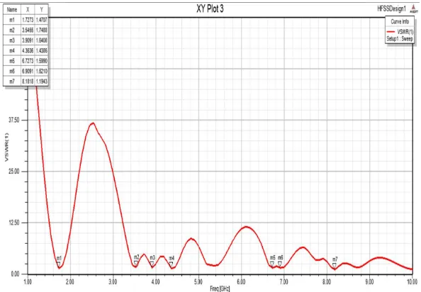
Return loss is an important parameter of antenna. It is the difference between forward and reflected power in dB. The return loss is the ratio of reflected power over transmitted power. The acceptable value of return loss is below -10dB for the antenna to work efficiently. The return v/s frequency curve of 0th, 1st and 2nd iteration are shown in Figure 4, 5 and 6 respectively. It is observed that min return loss is observed at 8.1 GHz i.e. -21.05 in 0th Iteration, at 5 GHz i.e. –17.68 in 1st Iteration and at 5.1 GHz i.e. -18.61 in 2nd Iteration of Proposed Antenna.
Moreover return loss and gain for various resonant frequencies is given in Table 2. A very low return loss can be achieved at frequency of 8.1GHz.
[image:3.612.162.451.476.707.2]Figure 5: Return loss of 1stiteration of Proposed Antenna
Figure 6: Return loss of 2nd iteration of Proposed Antenna
VSWR is Voltage Standing Wave Ratio it shows the impedance mismatch between the feeding system and antenna. Higher VSWR means higher mismatch. The acceptable value of VSWR is less than 2 and it is a dimension less quantity. The VSWR v/s frequency curve of 0th, 1st and 2nd iteration of proposed antenna are shown in Figure 7, 8 and 9 respectively. The comparisons of simulated results are shown in Table 2.
[image:4.612.158.455.500.706.2]Figure 8: VSWR v/s frequency curve of 1st iteration of proposed antenna
Figure 9: VSWR v/s frequency curve of 2nd iteration of proposed antenna
IV. GAIN
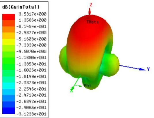
[image:5.612.205.406.567.712.2]The outcome of simulated results of return loss and gain confirms the good performance for proposed design of microstrip patch antenna. It can be seen from figure 1.3(a), 5.1dB is maximum gain obtained at 6.9GHz in 0th iteration, 5.2 dB is maximum gain obtained at 7 GHz in 1st iteration and 9.74 dB is maximum gain obtained at 8.5 GHz in 2nd iteration. Gain shows the directional capability and efficiency of antenna. The acceptable value of antenna gain is 3dB or more. The 3-D gain plot of proposed antenna for 0th, 1st and 2nditeration is shown in Figure 10, 11 and 12.
Figure 10.6 (b) Gain at 6.9 GHz
Figure 10.7 (c) Gain at 8.1 GHz
Figure 10 : Gain of 0th iteration of proposed antenna
[image:6.612.173.440.498.702.2]Figure 11.2 (b) Gain at 6.5 GHz
[image:7.612.193.418.73.393.2]Figure 11.3 (c) Gain at 7 GHz
[image:7.612.199.416.413.715.2]Figure 11: Gain of 1st iteration of proposed antenna
Figure 12.3 (a) Gain at 4.4 GHz
Figure 12.4 (c) Gain at 5.1 GHz
[image:8.612.39.579.225.428.2]Figure 12: Gain of 2nd iteration of proposed antenna
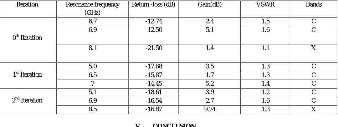
Table 2: Comparison of Various Iterations of Proposed Antenna Iteration Resonance frequency
(GHz)
Return -loss (dB) Gain(dB) VSWR Bands
0th Iteration
6.7 -12.74 2.4 1.5 C
6.9 -12.50 5.1 1.6 C
8.1 -21.50 1.4 1.1 X
1st Iteration
5.0 -17.68 3.5 1.3 C
6.5 -15.87 1.7 1.3 C
7 -14.45 5.2 1.4 C
2nd Iteration
5.1 -18.61 3.9 1.2 C
6.9 -16.54 2.7 1.6 C
8.5 -16.87 9.74 1.3 X
V. CONCLUSION
In this paper, a design of multiband microstrip patch antenna is proposed, which covers the frequency range between 2GHz and 9GHz. The return loss for all resonant frequency is -10 dB . The maximum gain is 9.74 dB at 8.5 GHz in second iteration. Seconditeration possess this is a tri band fractal antenna. The proposed antenna can be used for wireless applications wireless broadband transceiver which is applicable to mobile Wi max, fixed Wi max, RADAR applications including continuous wave pulsed, single polarisation, dual polarisation and air traffic control.
REFERENCES
[1] M.Sahoo, S.Pattnaik and S.Sahu, ”Design of compact UWB hexagonal monopole antenna with frequency notch characteristics,” International Conference on Circuit, Power and Computing Technologies (ICCPCT), 2015.
[2] Y. Kumar and S. Singh, “A Quad band hybrid fractal antenna for wireless applications,” IEEE, International Advance Computing Conference (IACC), pp. 730-733, 2015.
[3] M. M. M. Ali, A. M. Azmy and O. M. Haraz, “Design and implementation of reconfigurable quad-band microstrip antenna for MIMO wireless communication applications,” IEEE 31st National Radio Science Conference (NRSC), pp. 27-34, 2014.
[4] F.Daneshmandian, P.Dekhoda and A.Tavakoli, ”A miniaturization circularly polarised microstrip antenna for GPS applications,” IEEE 22nd Iranian Conference on Electrical Engineering (ICEE), pp.1653-1656,2014
[5] M.Susila.T.R.Rao and A.Gupta, ”A novel fractal antenna design for UWB wireless communications,”IEEE, International Microwave and RF Conference (IMaRC),pp.118-120,2014.
[6] N.Prema, Anil Kumar, “Design of multiband microstrip patch antenna for C and X” , optik 127 (2016)8812-8818
[7] P.S. Bakariya, S. Dwari, M. Sarkar, M.K. Mandal, ”Proximity-Coupled microstrip antenna for bluetooth, WiMAX, and WLAN applications,” IEEE AntennasWirel. Propag. Lett. 14 (2015).
[8] S.Behera and D.Barad, “A novel design of microstrip fractal antenna for wireless sensor network,” IEEE, Inernational Confrence of Power, Energy, Information and Communication, pp. 0470-0474,2015.
[9] T.Landeau, O.Losito, G.Palma, V.Portosi, A. Jouanneaux and F.Prudenzano, ”Multiband Rohmbus Monopole Antenna,” GeMic, pp.367-370,2015
[10] V.vaid and S.Agarwal, ”Bandwidth optimization using fractal geometry on rectangular microstrip patch antenna with DGS for wireless applications,” International conference on medical Imaging, M-health and Emerging Communication Systems (MedCom), pp.162-167,2014