Microstructures and Fusing Electrical Current
of Microelectronic Sn-9Zn-(0.25RE) Solders
Fei-Yi Hung
1;*, Truan-Sheng Lui
2;*, Li-Hui Chen
2and Kung-An Lan
21
Institute of Nanotechnology and Microsystems Engineering, Center for Micro/Nano Science and Technology, National Cheng Kung University, Tainan 701, Taiwan, R.O. China
2Department of Materials Science and Engineering, National Cheng Kung University, Center for Micro/Nano Science and Technology, Tainan 701, Taiwan, R.O. China
Both Sn-9Zn and Sn-9Zn-0.25RE solders were used to investigate the effect of RE (rare earth elements) addition on their solidification structures and electrical current properties. The results indicate that adding RE not only made the needle-like Zn-rich phases finer, but also caused the Sn-Zn eutectic phases to decrease. RE elements existed mostly in the-Sn phases and could not form intermetallic compounds. After direct current (DC) testing and electrical conductivity (%IACS) testing, the fusing electrical direct current density of the 0.25RE solder was higher than the Sn-9Zn solder, however, the electrical conductivity had an inverse tendency. Also, the RE element addition restrained electromigration and enhanced diffusion to occur easily in the Sn-9Zn solder. [doi:10.2320/matertrans.MF200801]
(Received August 21, 2007; Accepted February 27, 2008; Published April 9, 2008)
Keywords: tin-zinc, lead-free solder, rare earth (RE)
1. Introduction
Under electrical current testing of solders, electromigra-tion and enhanced diffusion are induced, intermetallic compounds (IMC) grow irregularly, and the temperature is raised by the thermoelectric effect,1–4) any of which may cause failure of the solders. For the applied science of electrical current, most studies have focused mainly on the electromigration mechanism in lead-free solders,5–7) while the fusing mechanism has been almost ignored. For this reason, the application of the safety fuse wire for lead-free solder materials still has some limitations. Because thermo-electric behavior of the thermo-electrical current always occurs and negatively affects the relevant properties of solders, the fusing characteristics of the solder materials still need to be examined.
Because the Sn-Zn eutectic alloy has a low melting point (198C), excellent mechanical properties and acceptable
costs,8,9)it has been recognized as one of the best choices as a
lead-free solder. In addition, relevant reports10–14) have shown that the drop resistance, wetting and hardness of Sn based solders can be enhanced by a very small addition of La, Ce, etc. But, the effect of rare earth elements (RE) on the fusing mechanism of lead-free solders has not yet been discussed. Owing to the microstructure and electrical conductivity being closely related to the solder fusing characteristics and the solder workability, this study uses near-eutectic Sn-9Zn-(0.25RE) solders not only to analyze the microstructural characteristics, but also investigate the effect of RE (rare earth element) addition on fusing electrical current under direct current (DC) testing to explore the potential for use as a lead-free solder.
2. Experimental Procedure
Near-eutectic Sn-9 mass%Zn-(0.25 mass%RE) solders
were prepared by melting pure tin, pure zinc and rare earth elements in a high-frequency induction furnace. The chemi-cal composition of the mixed RE is shown in Table 1. The alloy ingots were then remelted and cast into a Y-shaped graphite mold. In order to collect the electrical current test data, rectangular specimens (gauge length section:
20mm5mm0:8mm) were also prepared. An Electrical Conductivity Analyzer was used to measure the electrical conductivity (%IACS) of the solders. The %IACS is defined as the percentage ratio of international standard copper electrical conductivity to the electrical conductivity of the material used. The electrical current tests were performed on high electrical apparatus with a Programmable Logic Con-troller (PLC) and the increasing rate of electrical current was controlled at 1–2.4 A/s. Direct current (DC) was used to collect the values of the fusing electrical current. Before and after current testing, the microstructures of the solders were determined quantitatively using an image analyzer and X-ray diffraction. A comparison of the microstructural variations was performed on the non-electrical current specimens and the electrical current specimens. The electrical current was held at 40 A (direct electrical current density = 1000 A/cm2)
for 12 s. Each analysis datum was the average of at least 5–7 test results.
3. Results and Discussion
[image:1.595.306.551.337.381.2]3.1 Electrical conductivity and fusing electrical current Figure 1 shows the microstructures of the Sn-9Zn solder and the Sn-9Zn-0.25RE solder. The needle-like Zn-rich phases were finer, Sn-Zn eutectic phases decreased and-Sn phases increased with addition of RE. In Fig. 1(b), many
Table 1 Chemical composition of RE (mass%).
Content of mixed rare earth
La Pr Nd Ce
302 51 51 Bal.
*Corresponding author, E-mail: [email protected];
finer particle-like precipitated phases (RE congregated) are observed (see EDS of Fig. 1(c)). Notably, the present precipitated phases were almost all Ce-La intermetallic compounds (IMC), that have a higher melting point than Sn matrix. During the casting process, the Ce-La IMCs solidified through a precipitation process first, then the other phases solidified. In Fig. 1(b) and Fig. 1(c), we confirm that the finer particle-like phases were Ce-La intermetallic compounds containing a little Sn and Zn. Precipitated Ce-La IMCs
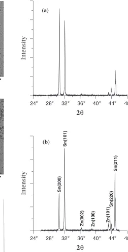
produced with Sn-Zn eutectic phase dispersing in the matrix was the solidification mechanism. Figure 2 shows the X-ray diffraction patterns of the Sn-9Zn and Sn-9Zn-0.25RE solders. According to the microstructural observations (Fig. 1), the Sn-9Zn specimen and Sn-9Zn-0.25RE specimen possessed similar near-eutectic structures except for the precipitated Ce-La IMCs. For the Sn-9Zn-0.25RE specimen, the precipitated Ce-La IMCs congregated near the needle-like Zn-rich phases. Because the content of Ce-La IMC was low (0.25 mass%), the X-ray diffraction patterns (Fig. 2) showed only that formation phases were similar in both solders.
The electrical conductivity (%IACS) of the Sn-9Zn-(0.25RE) solders is shown in Fig. 3. When 0.25 mass% RE was added, the electrical conductivity of the specimen
(c)
(a)
30
µ
m
(b)
30
µ
m
Fig. 1 Microstructures of solders: (a) Sn-9Zn, (b) Sn-9Zn-0.25RE, (c) EDX of the particle-like precipitated in (b).
°
Sn(211)
Sn(220)
Zn(101)
Zn(100)
Zn(002)
Sn(101)
Sn(200)
24
θ
Intensity
Intensity
2
(a)
2
(b)
° 32° 36° 40° 44° 48° 28
θ
°
24 28° 32° 36° 40° 44° 48°
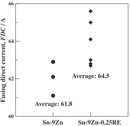
[image:2.595.51.293.69.616.2] [image:2.595.277.529.72.565.2]became lower than that of the Sn-9Zn specimen. Notably, the Sn-9Zn-0.25RE specimen possessed a greater fusing direct current (FDC) value than the Sn-9Zn specimen (see Fig. 4). In fact, a very small RE addition (0.05 mass% RE, not given here) decreased the electrical conductivity of the Sn-9Zn near-eutectic alloy (conductivity of Sn-9Zn near-eutectic was 16.93%IACS). These results and the pure metal property15)
also explain that the very small amount of RE led to an increase in the solid solution atom content (impurity effect) and finer precipitated RE in -Sn phase, resulting in a reduction in the electrical conductivity. While the electrical current effect was active, adding 0.25 mass% RE led to a greater fusing electrical current value (Fig. 4).
In fact, some literature13,14,16,17)indicates that the addition of RE not only increases the grain boundary energy of Sn
based matrix (RE congregated), but also restrains the growth of IMCs. So, the effect of solid solution atoms and micro-segregation RE cause the electrical conductivity to decrease. For some conducting wires (Ag wire or Cu wire), the heat of fusion increases with raising the melting point. However, metals with a high heat of fusion are not certain to have high electrical conductivity.15)According to relevant references18) and previous DSC data (Sn-9Zn: 198.47C and Sn-9Zn-0.25RE: 199.00C), it can be inferred that adding 0.25 mass%
RE and therefore inducing structural variations (Sn-Zn eutectic decrease and fine IMC) and an increase in the melting point must be one reason why the limit of the fusing current was raised.
3.2 Fusing mechanism
To avoid the solders fusing under high electrical current testing, this study used a fixed electrical current (DC) of 40 A (direct electrical current density = 1000 A/cm2) on the Sn-9Zn-(0.25RE) solders to examine the microstructural variations (the current passed through the specimen for 12 s). The experimental results reveal that the microstructure of the Sn-9Zn specimen experienced a change at the 12 s mark (see Fig. 5). Comparing Fig. 5(a) with Fig. 5(b), the content 16
16.4 16.8 17.2 17.6
Sn-9Zn Sn-9Zn-0.25RE
Electrical conducti
vity
,
EC
/ %IA
CS
Average: 16.9
Average: 16.4
Fig. 3 Electrical conductivity (%IACS) of the Sn-9Zn and Sn-9Zn-0.25RE solders.
60 62 64 66
Sn-9Zn
Sn-9Zn-0.25RE
Fusing dir
ect curr
ent,
FDC
/
A
Average: 61.8
Average: 64.5
Fig. 4 Fusing electrical direct current (DC) of the Sn-9Zn and Sn-9Zn-0.25RE solders.
(a)
(b)
30
µ
m
30
µ
m
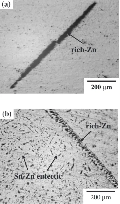
[image:3.595.308.544.70.446.2] [image:3.595.55.284.71.284.2] [image:3.595.56.285.336.558.2]of Sn-rich phase had decreased and the Sn-Zn eutectic areas had increased after the electrical current test. In order to enhance this effect, we selected an electrical current (DC) of 50 A for 8 s to perform the current test. Notably, we used a higher electrical current (50 A: in Fig. 6) instead of that in Fig. 5 (40 A), and different fields were observed before and after the current test in Fig. 6. The results also revealed that the morphology of the needle-like Zn-rich phase still trans-formed from needle-like to particle-like under current testing (see Fig. 6, the particle-like phase was a Sn-Zn eutectic phase). According to previous data,19) the microstructure of the Sn-9Zn specimen did not change obviously at 130C
(oxygen insulation: oil bath treatment) for 300 s. Even when the temperature was increased to 180C and held at 600 s, the
microstructure still showed no phase transformation (melting point: 198C). This also indicates that this phase
trans-formation was not only induced by the thermal effect. The most likely explanation for this is a combination of the electromigration effect and enhanced diffusion. Notably, RE addition prevented electromigration and diffusion from occurring easily.
Figure 7 shows the microstructures of the Sn-9Zn-0.25RE specimens (the conditions are the same as Fig. 5). There was no obvious change in the microstructure of the Sn-9Zn-0.25RE solder after 12 s at 40 A (Fig. 7(b)). After DC testing, the microstructure of the Sn-9Zn specimen underwent a
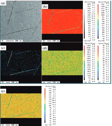
[image:4.595.312.543.70.254.2]change, while the microstructure of the Sn-9Zn-0.25RE specimen experienced no variation during DC testing. Backscattering electron images (EPMA) of the Sn-9Zn-0.25RE solder after electrical current testing are shown in Fig. 8. Except for precipitated RE particles, the results indicate that RE elements were still solid solution in the-Sn matrix. So, it is safe to say that the effect of RE addition increased the area fraction of -Sn and enhanced the solid solution effect. The impure -Sn and microsegregation of REs were the main reasons why the electrical conductivity deteriorated. However, a very small RE addition not only inhibited the electrical current phase transformation, but also raised the limit of the fusing electrical current.
4. Conclusions
When 0.25 mass% RE was added into to the Sn-9Zn solders, the needle-like Zn-rich phases became finer, Sn-Zn eutectic phases decreased and -Sn phases increased. In addition, there was a reduction in electrical conductivity because of RE addition, and the solid solution effect prolonged the duration of electromigration and diffusion to raise the fusing electrical resistance.
rich-Zn
200
µ
m
200
µ
m
rich-Zn
Sn-Zn eutectic
(a)
(b)
Fig. 6 Comparing the microstructure of the Sn-9Zn eutectic solder: (a) before test and (b) after test (electrical current condition: 50 A for 8 s).
(a)
(b)
30
µ
m
30
µ
m
[image:4.595.66.274.75.426.2] [image:4.595.308.543.78.437.2] [image:4.595.312.542.266.446.2]Acknowledgements
The authors are grateful to National Cheng Kung Uni-versity, the Center for Micro/Nano Science and Technology (NCKU Project of Promoting Academic Excellence & Developing World Class Research Center: D96-2700) and the Chinese National Science Council for its financial support (Contract: NSC-96-2622-E-006-024-CC3).
REFERENCES
1) T. Y. Lee, K. N. Tu, S. M. Kuo and D. R. Frear: J. Applied Physics.89 (2001) 3189–3194.
2) C. Y. Liu, C. Chen, C. N. Liao and K. N. Tu: Applied Physics Letter75 (1999) 58–60.
3) C. Y. Liu, C. Chen and K. N. Tu: J. Applied Physics 88 (2000) 5703–5709.
4) D. M. Rowe:Thermoelectric materials, Handbook of Thermoelectric, (CRC, New York, 1995) pp. 395–396.
5) H. Ye, D. C. Hopkins and C. Basaran: Proc. SPIE 4931 (2002) 427–432.
6) J. M. Song, T. S. Lui, L. H. Chen and D. Y. Tsai: Journal of Electronic
Materials32(2003) 1501–1508.
7) J. M. Song, F. I. Li, T. S. Lui and L. H. Chen: J. Mater. Res.19(2004) 2665–2672.
8) J. M. Song, G. F. Lan, T. S. Lui and L. H. Chen: Scripta Materialia48 (2003) 1047–1051.
9) C. M. L. Wu, C. M. T. Law, D. Q. Yu and L. Wang: J. of Electronic materials32(2003) 63–69.
10) C. M. L. Wu, C. M. T. Law, D. Q. Yu and L. Wang: J. of Electronic Materials32(2003) 63–74.
11) W. Xiuqin, H. Huizhen, Z. Lang and Z. Meng: Journal of Rare Earths 23(2005) 220–223.
12) M. A. Dudek, R. S. Sidhiu and N. Chawla: JOM (2006) 57–62. 13) C. M. L. Wu, D. Q. Yu, C. M. T. Law and L. Wang: J. of Electronic
Materials31(2002) 921–927.
14) http://www.matter-antimatter.com/periodic table.htm.
15) C. M. L. Wu, D. Q. Yu, C. M. T. Law and L. Wang: J. Mater. Res.17, No. 12 (2002) 3146–3154.
16) L. Wang, D. Q. Zhao and M. L. Huang: Materials Letters56(2002) 1039–1042.
17) Y. L. Tsai, W. S. Hwang, H. S. Wang and M. H. Wu: International Journal of Cast Metals Research15(2002) 181–186.
18) F. Y. Hung, Z. R. Wang, T. S. Lui and L. H. Chen: Mater. Trans.46 (2005) 1820–1824.
19) F. Y. Hung, Z. R. Wang, S. M. Huang, L. H. Chen and T. S. Lui: J. of Alloys and Compounds420(2006) 193–198.
(a)
(b)
(c)
(d)
(e)
[image:5.595.113.486.71.489.2]