Non-Conductive Adhesive (NCA) Trapping Study in Chip
on Glass Joints Fabricated Using Sn Bumps and NCA
Sang-Mok Lee, Byeung-Gee Kim and Young-Ho Kim
*Division of Materials Science & Engineering, Hanyang University, 17 Haengdang-dong, Seongdong-gu, Seoul, 133-791, Korea
Chip-on-glass (COG) bonding using a nonconductive adhesive (NCA) and the entrapment of NCA and fillers in the COG joints were studied. Sn was used as a bump material because it has a higher propensity of plastic deformation than an Au bump. Three types of Sn bumps were fabricated, electroplated Sn bumps, reflowed Sn bumps, and coined Sn bumps. Three types of NCAs were applied during COG bonding. The reflowed bump had the least amount of trapped NCA with fillers among the bumps studied. The NCA with the lowest viscosity was trapped the least compared to the other NCAs. The electrical test results showed that contact resistance increased with increasing amounts of trapped NCA with fillers in the COG joint. [doi:10.2320/matertrans.MRA2008071]
(Received February 27, 2008; Accepted June 3, 2008; Published July 30, 2008)
Keywords: tin bump, nonconductive adhesive, chip on glass, electro plating, flip chip
1. Introduction
Chip on glass (COG) bonding is widely used in liquid crystal display (LCD) driver integrated circuit (IC) pack-aging.1,2) In COG technology, the driver IC is directly mounted on the LCD module by the flip chip method. COG technology offers both the thinnest packaging options and the smallest packaging area. COG technology also features several other advantages, such as improvements in multipin capability and in electrical properties. Furthermore, COG technology permits high density substrate bonding over short distances and is, therefore, suitable for packaging high speed and high performance devices.3) COG bonding with a fine pitch of 30mmhas been successful.4,5)
The most common COG bonding technology is based on an anisotropic conductive film (ACF).6–8) The principle of COG bonding using ACF is that the electrical connections are established through conductive particles and the mechanical interconnections are maintained by the adhesive.6) The advantage of ACF technology compared with soldering is flexibility, the capability to produce fine pitch interconnec-tions, lead-free bonding, cheaper manufacturing, and proc-essing at lower temperatures.9,10)
When the COG bonding technology using ACF is applied to mount a fine pitch (<50mm) LCD driver IC, an electrical short is sometimes generated between the adjacent bumps due to the electrical bridging by conductive particle ag-glomeration between the bumps.7)Because of this, contact resistances either increase or the interconnect will be prone to opening due to the reduction in pitch and contact size.11)
COG bonding technology using NCAs has been recently reported.4,5,12,13) The bonding method using an NCA has various advantages by facilitating fine pitch bonding, reducing manufacturing costs, and achieving superior elec-tric properties by a reduced contact resistance between the metal bump and the electrode pad. Instead of relying on the mediate connection of conductive particles squeezed between the bump and electrode pads, this process realizes direct electrical contact and thereby increases the contact area, which then reduces the contact resistance. In this
bonding method, the bonding process can be performed at a relatively low temperature in a simplified manner since it can be performed at the adhesive’s curing temperature.13,14)
Conventionally, electro-less Au/Ni bumps, electroplated gold bumps, and polymer based composite-bumps are used as the bump material.12,15–17)Sn bumps have a lower hardness and higher plastic deformation capability than an Au bump. Several articles have been devoted to the study of COG technology using Sn bumps.4,5,13)
Since the metal bumps are in direct contact with the pads on the glass substrate in this particular NCA technology, a trapping phenomenon may occur in which a part of the NCA remains between the bump and the pad.18,19) The trapped NCA may induce an increase in the contact resistance between the bump and the metal electrode and in the worst case, cause a open circuit. Therefore, it is important to reduce the amount of trapped NCA. In this paper, we investigate the effects of the Sn bump types and NCA on overall NCA trapping. We used large size bumps (100mm
100mm) to measure the amount of NCA trapping more precisely. Three different types of Sn bumps were fabricated; electroplated Sn bumps, reflowed Sn bumps, and coined Sn bumps after electroplating. The electrical properties of the COG joints fabricated using reflowed Sn bumps and NCAs are also presented.
2. Experimental Procedure
Ti (50 nm), Cu (1mm), and Au (50 nm) thin films were deposited sequentially on an oxidized Si wafer using a DC magnetron sputtering system as under bump metallization (UBM) and interconnection lines. The metal patterns on the chip were fabricated through a photolithographic process and wet chemical etching methods.
Three types of Sn bumps were made on the UBM pads. The 20mm thick electroplated Sn bumps were fabricated by electroplating. The coined Sn bumps were fabricated by flattening the electroplated bumps using a thermo-compres-sion bonder. The reflowed Sn bumps were formed by reflowing the electroplated bumps at 270C for 20 sec in the forming gas (95 vol%N2 + 5 vol%H2) using a rapid thermal annealing system.
*Corresponding author, E-mail: kimyh@hanyang.ac.kr
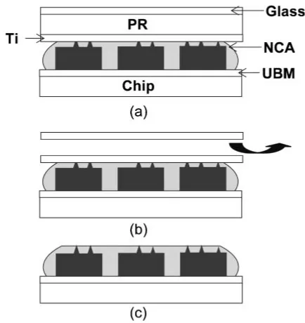
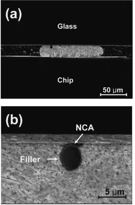
COG bonding was performed at 150C under 100 MPa using a thermo-compression bonder after NCA was dis-pensed over the Sn bumps on the Si chip. Three different NCAs were used and their properties are summarized in Table 1. The holding time at 150C was 45 sec for NCA-A and 15 sec for NCA-B and NCA-C. Figure 1 shows one example of the bonding process with reflowed Sn bumps. Two types of metallization were formed on the glass substrate (Corning 1731 glass). For the NCA trapping study, the photoresist (PR) (6mm) and Ti (50 nm) were deposited on the glass substrates. Then a simulated bonding was performed using Sn bumps on Si chip and Ti/PR/glass substrates. After bonding the Sn bumps were separated from
the glass substrates by dissolving the PR. Then the Ti layer on the Sn bump was removed by wet chemical etching in 5% HF. Figure 2 contains a schematic diagram of the NCA trapping experiment. NCA and filler trapping was observed using a back-scattered electron (BSE) image. A quantitative analysis of NCA trapping was done using an image analyzer. For the contact resistance study, a Ti (50 nm), Cu (1mm), and Au (50 nm) layer was inserted between the Indium Tin Oxide (ITO) and glass to reduce the interconnect resistance. The bonding was preformed between the Sn bump on the Si chip and ITO on glass. The contact resistance of an individual joint was measured using the four-point probe method. The details of the four point probe method have been described previously.20)
3. Results
3.1 Bump formation
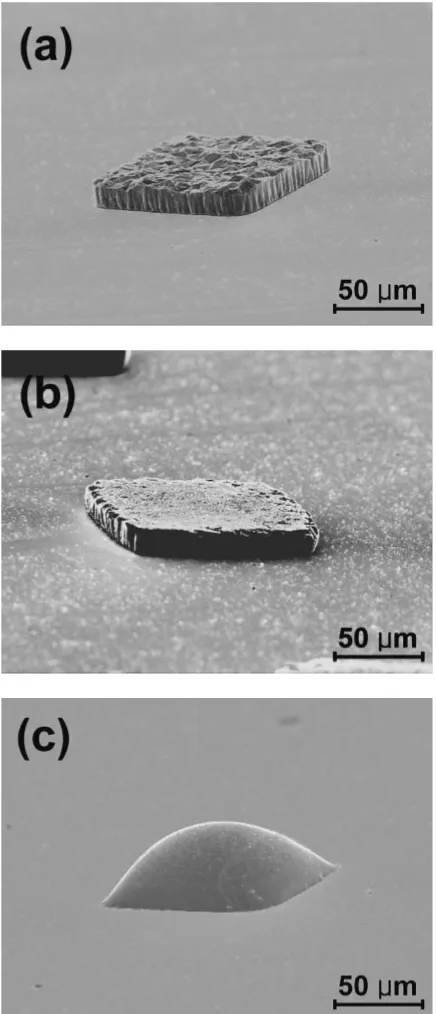
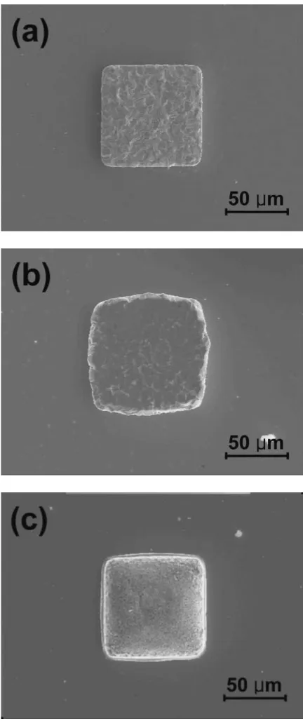
The secondary electron (SE) images of three types of Sn bumps are shown in Fig. 3. Sn bumps were well formed in an area array pattern and there was no bridging between the neighboring bumps. Figure 4 shows magnified images depicting each Sn bump. Also, the Top view images of the Sn bumps are presented in Fig. 5. Figure 6 contains enlarged images of Fig. 5. The morphology of the electro-plated Sn bumps can be seen in Figs. 4(a), 5(a), and 6(a). Average height of the electroplated Sn bumps was about 20mm. The surface of the electroplated bumps was relatively rough. Figures 4(b), 5(b), and 6(b) show the morphology of the coined Sn bumps. The average height of the coined Sn bumps decreased from 20mmto 16mmafter coining. The surface of the coined Sn bumps was smoother than the electroplated Sn bump. Figures 4(c), 5(c), and 6(c) show the morphology of the reflowed Sn bumps. After reflowing, the peak height of the reflowed Sn bumps was about 40mm since semi-spheroid bumps were formed to
NCA-C Fluoropolymer 8,500 98 174 31
TM: 5 rpm
TM: Test method
Fig. 1 An illustration of the COG bonding using reflowed Sn bumps and NCA. (a) Formation of electroplated Sn bumps. (b) Reflowing of electroplated Sn bumps. (c) NCA dispensing and placement of substrates. (d) Deformation of the Sn bumps during the bonding and curing of NCA.
[image:2.595.316.533.70.300.2] [image:2.595.47.294.84.205.2] [image:2.595.61.277.238.564.2]reduce the surface energy. The reflowed bumps have the smoothest surface among the bumps fabricated in this experiment. Top view SE images in Fig. 5 show the size of a Sn bump. The size of the electroplated Sn bumps and reflowed Sn bumps was about 100mm100mm square. And the size of coined Sn bumps increased to about 110mm110mm square because the Sn bumps were squeezed during the coining process.
3.2 NCA trapping
After bonding at 150C between Sn bumps and the Ti/ PR/glass substrate, the Sn bumps were separated from the substrates by removing the PR and Ti layer. The BSE
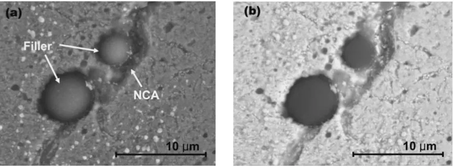
images of the bump surfaces and trapped NCA and fillers are shown in Figs. 7, 8, and 9. Compared with Fig. 5, the overall size of the bumps in Figs. 7, 8, and 9 was increased after bonding due to excessive plastic deformation of the Sn bumps. Trapped NCA with fillers was clearly seen in the BSE images. In the BSE images, the Sn phase appeared to be lighter than the NCA since the BSE signal increased with the concentration of the heavier element.11) Thus the bright region represents the Sn bump surface and the dark region represents the NCA and fillers. It is obvious that the reflowed bumps have the lowest amount of trapped NCA with fillers amongst the three bump types. Figure 10 represents a typical example which shows the filler and
Fig. 3 SE images showing 3 types Sn bumps, (a) electroplated Sn bump, (b) coined Sn bump, and (c) reflowed Sn bump.
[image:3.595.60.277.70.583.2] [image:3.595.318.536.72.579.2]NCA trapped in the Sn interface. Bonding was made using reflowed bumps and NCA-A. Spherical silica fillers em-bedded on the Sn bump surface are clearly seen. If the fillers are embedded in the Sn interface, a gap between the fillers and the Sn bump will be formed and NCA may flow into the gap more easily.
A quantitative analysis of the amount of trapped NCA with fillers was carried out using an image analyzer and the results are given in Fig. 11. The trapped amount of NCA and fillers was calculated as a ratio of the area of trapped NCA with fillers to the whole area of the Sn surface. The reflowed bump specimens had the lowest amount of trapped NCA with fillers
amongst the three types of fabricated bumps studied in this experiment. The trapped amount of NCA and fillers in the reflowed bumps was below 8% in all specimens regardless of NCA type. The NCA and filler trapping in the coined bump specimens was less than that of the electroplated bump specimens. The amount of trapped with fillers in the NCA-C was the lowest of all specimens, regardless of bump types.
3.3 Contact resistance
Since NCA and filler trapping was lowest in the reflowed bumps, COG bonding was performed between the reflowed Sn bumps on the Si wafer and the ITO/Au/Cu/Ti glass substrate using three different NCAs. The electrical
measure-Fig. 5 SE images showing top view of three types of Sn bumps before bonding, (a) electroplated Sn bump, (b) coined Sn bump, and (c) reflowed Sn bump.
[image:4.595.60.276.70.584.2] [image:4.595.317.536.76.582.2]Fig. 7 BSE images showing the bumps’ surface after bonding using NCA-A, (a) electroplated Sn bump, (b) coined Sn bump, and (c) reflowed Sn bump.
Fig. 8 BSE images showing the bumps surface after bonding using NCA-B, (a) electroplated Sn bump, (b) coined Sn bump, and (c) reflowed Sn bump.
[image:5.595.121.476.73.183.2]Fig. 9 BSE images showing the bumps surface after bonding using NCA-C, (a) electroplated Sn bump, (b) coined Sn bump, and (c) reflowed Sn bump.
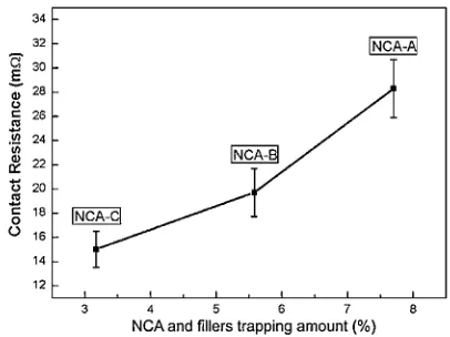
[image:5.595.124.476.239.348.2] [image:5.595.123.475.409.519.2] [image:5.595.77.523.594.758.2]ments showed that the average contact resistance of each joint was 28 mfor NCA-A, 19 mfor NCA-B, and 15 m for NCA-C. Not one joint failed electrically. The cross sectional SE images of the COG joints between the reflowed Sn bumps and glass substrates are shown in Figs. 12 and 13. The UBM on the Si wafer, deformed Sn bumps and interconnection layers on glass substrates are clearly seen in Figs. 12 and 13. Sn bumps and ITO pads are in direct contact in the magnified images showing the Sn/ITO interfaces. These images demonstrated that the Si chip and glass substrate were successfully bonded through the
defor-mation of Sn bumps. After bonding, the height of the reflowed Sn bump was reduced from 40mmto 17mm. Heavy deformation of reflowed Sn bumps was clearly seen and a contact was successfully made between the Sn bump and the ITO/Au/Cu/Ti on the glass substrate. Sometimes, it was observed that the NCA and fillers were only trapped locally. An example is shown in Fig. 13. NCA and fillers were trapped at the bump/ITO interface. A spherical segment of filler was trapped in the Sn bump and the NCA remained between the ITO and filler. The direct contact between the Sn bump and ITO failed in the region where the NCA was trapped.
Contact resistance values of the COG joint are plotted with respect to the amount of trapped NCA and fillers in Fig. 14. The relationship between contact resistance values and the NCA and filler trapping amount is clearly visible. Contact resistance of the COG joints increased with the amount of trapped NCA and fillers.
4. Discussion
[image:6.595.63.277.70.223.2]Our results showed that Sn bumps and ITO pads were joined successfully through the deformation of Sn bumps during bonding. The contact resistance of COG joints using reflowed bumps was very low in all specimens. Sn bumps were easily deformed and Sn bump deformation can compensate for bump height variations.13)
Fig. 11 Average quantity analysis of % NCA and fillers trapped between the chip and glass substrate according to different types of Sn bumps.
[image:6.595.317.539.73.411.2]Fig. 12 SE image showing the cross section of a COG joint using NCA-A. (No NCA was trapped in the bump.)
[image:6.595.60.280.271.610.2]The surface roughness of Sn bumps influenced the NCA and filler trapping. The coining process deformed the Sn bump surface and decreased the surface roughness.21) A lower amount of NCA and filler trapping was observed during bonding with a smoother surface, as seen in Fig. 11. The amount of trapped NCA and fillers was lowest in the reflowed bump. A semi-spherical bump initiated point contact with the substrate during bonding. Further pressuring increased the contact area due to the deformation of the Sn bump and NCA was squeezed out from the Sn bump (See Fig. 1(d)). The bump shape was more effective to reduce the NCA and filler trapping than surface roughness of bumps since the reflowed bumps had much less amount of trapped NCA with fillers.
The NCA type also strongly influenced NCA trapping. NCA with a lower viscosity flows more readily during bonding and traps less.22) NCA contains fillers to control thermal expansion.22,23) When the filler is harder, it may easily embed in the soft Sn bump during bonding and NCA can easily be trapped near the filler as shown in Fig. 10. As a result, NCA was trapped less in the COG joint formed using NCA-C, which has a lower viscosity, and contains softer fluoropolymer fillers.
In the NCA and filler trapped region, the contact between the Sn bump and ITO failed. The loss of contact area due to NCA and fillers caused an increase of the contact resist-ance.12)The less NCA and filler trapping occurs, the lower the contact resistance will be, as shown in Fig. 11.
5. Conclusion
We investigated NCA trapping in the COG joints formed using Sn bumps and various NCAs. The effect of Sn bump types on NCA trapping was studied with three different types of NCAs. The reflowed bump allowed the least trapping of NCA and fillers among the bumps studied. This was because
the spherical bumps squeezed out the NCA during bonding. The lowest viscosity NCA was trapped less than the other NCAs. The contact resistance of the COG joints formed with reflowed Sn bumps was very low regardless of NCA type. The contact resistance of the COG joints was closely related to NCA trapping.
Acknowledgements
This research was supported by a grant from the Information Display R&D Center, one of the 21st Century Frontier R&D Program funded by the Ministry of Knowl-edge Economy, Republic of Korea. The authors would like to thank Loctite for providing the NCAs.
REFERENCES
1) J.-H. Choi, K.-Y. Lee, S.-W. Jun, Y.-H. Kim and T.-S. Oh: Mater. Trans.46(2005) 1042–1046.
2) H. Kristiansen and J.-Liu: IEEE Tran. Comp. Packag. Manufact. Technol. A21(1998) 208–214.
3) J. C. Hwang: IEEE Tran. Comp. Packag. Manufact. Technol. A18
(1995) 458–461.
4) S. Y. Kim, T.-S. Oh, W. J. Lee and Y.-H. Kim: Proc. Int. Conf. On Electron. Packag. Techno. (2006) 414–417.
5) S.-M. Chung and Y.-H. Kim: Mater. Trans.48(2007) 37–43. 6) P. Savolainen: Proc. 9th Int’l Sympo. On Adv. Packag. Mater. (2004)
7–10.
7) M. Y. Yim, J. S. Hwang and K. W. Paik: Int. J. Adhes. Adhes.27(2007) 77–84.
8) I. Watanabe, Y. Gotoh and K. Kogayashi: Proc. Int. Meet. Information Display (2001) 553–555.
9) J.-W. Kim, W.-C. Moon and S.-B. Jung: Microelectron. Eng.83(2006) 2335–2340.
10) C. W. Tan, Y. C. Chan and N. H. Yeung: Microelectron. Reliab.43
(2003) 481–486.
11) U.-B. Kang and Y.-H. Kim: IEEE Trans. Compo. & Packag. Techno.
27(2004) 254–258.
12) Y.-T. Hsieh: Int’l Sympo. On Electro. Mater. & Packag. (2002) 157–160.
13) Z. G. Chen and Y.-H. Kim: Displays.27(2006) 130–135.
14) M.-J. Yim and K. W. Paik: IEEE Trans. Compo. & Packag. Techno.21
(1998) 226–234.
15) H.-C. Cheng, C.-L. Ho, K.-N. Chiang and S.-M. Chang: IEEE Trans. Compo. & Packag. Techno.27(2004) 398–410.
16) S.-M. Chang, J.-H. Jou, H.-Y. Lin and C.-Y. Wu: Proc. 5th Asian. Sympo. On Inf. Display. (1999) 79–83.
17) J. Vanfleteren, B. Vandecasteele and T. Podprocky: Proc. 4th Electron. Packag. Techno. Conf. (2002) 139–143.
18) S. Kawamoto and O. Suzki: Proc. Int. Conf. On Electron. Packag. (2005) 33–37.
19) H. Lu, K. C. Hung, S. Stoyanov, C. Bailey and Y. C. Chan: Microelectron. Reliab. (2002) 1025–1212.
20) S.-H. Lee, H.-R. Roh, Z. G. Chen and Y.-H. Kim: J. Electron. Mater.34
(2005) 1446–1454.
21) J.-W. Nah, K. W. Paik, T.-K. Hwang and W.-H. Kim: IEEE Trans. Compo. & Packag. Techno.26(2003) 166–172.
22) K.-W. Jang, W.-S Kwon, M.-J. Yim and K.-W. Paik: Journal of the Microelectronics & Packaging Society10(2003) 9–17.
[image:7.595.66.269.70.222.2]23) M. J. Yim and K. W. Paik: Electron. Mater. Lett.2(2006) 183–194. Fig. 14 Relationship between trapped amount of NCA and fillers and