Kinetics of Reactive Diffusion in the Co
/
Zn System at Solid-State Temperatures
Yoshiki Takamatsu
1, Minho O
2and Masanori Kajihara
2,*1Graduate School, Tokyo Institute of Technology, Yokohama 226–8502, Japan
2Department of Materials Science and Engineering, Tokyo Institute of Technology, Yokohama 226–8502, Japan
The kinetics of reactive diffusion in the Co/Zn system was experimentally examined at solid-state temperatures. In this experiment, sand-wich Zn/Co/Zn diffusion couples were prepared by a diffusion bonding technique, and then isothermally annealed in the temperature range of 523–573 K for various times up to 211 h. Owing to annealing, an intermetallic layer consisting of the γ, γ1 and γ2 phases was formed at the
original interface in the diffusion couple, where the thickness is much smaller for the γ and γ1 phases than for the γ2 phase. Thus, the γ2 phase
predominantly governs the overall growth of the intermetallic layer. The total thickness of the intermetallic layer increases in proportion to a power function of the annealing time. The exponent of the power function takes values of 0.54–0.56 at 523–548 K and that of 0.85 at 573 K. Consequently, volume diffusion mainly controls the layer growth at 523–548 K, but interface reaction as well as volume diffusion contributes to the rate-controlling process at 573 K. [doi:10.2320/matertrans.M2016416]
(Received November 21, 2016; Accepted January 30, 2017; Published March 10, 2017) Keywords: reactive diffusion, metallization, solder, conductor, intermetallic compounds
1. Introduction
In the binary Sn–Zn system, the eutectic reaction L → Sn + Zn occurs at a temperature of Te = 472 K.1) Here, the concen-tration of Zn in the liquid (L) phase is 15 at% (9 mass%), the solubility of Zn in the Sn phase is smaller than 1 at%, and that of Sn in the Zn phase is negligible. Since the eutectic
tem-perature Te is much lower than the melting temperature of
pure Sn with Tm = 505 K, the eutectic Sn–Zn alloy is used as a Pb-free Sn-base solder with low-melting temperature in the electronics industry.2–8) On the other hand, the scaling-down of three-dimensional integration for electronic device results in decreasing bond pad pitch and smaller solder ball diameter. As an under bump metallization (UBM) material, Cu is wide-ly used in electronics interconnection and packaging.9–13) Re-cently, the capability of Co as a new UBM material for Sn-base solder bump has been investigated by many
research-ers.14–22) If Co is interconnected with the Sn–Zn solder, Co–
Sn and Co–Zn compounds may be formed at the interconnec-tion during soldering, and then will gradually grow due to solid-state heating under usual energization conditions. Since such intermetallic compounds are generally brittle and pos-sess high electrical resistivities, the compound growth deteri-orates the electrical and mechanical properties of the inter-connection. Thus, for application of Co, reliable information on the kinetics of reactive diffusion between Co and the Sn– Zn solder at solid-state temperatures is essentially important. The solid-state reactive diffusion in the Co/Sn system was experimentally observed in a previous study.23) In that exper-iment, Sn/Co/Sn diffusion couples were prepared by a diffu-sion bonding technique, and then isothermally annealed in the temperature range of T = 433–473 K. In this temperature range, an intermetallic layer composed of CoSn3 is formed at
the original Co/Sn interface in the diffusion couple. The
mean thickness of the CoSn3 layer is proportional to a power function of the annealing time. The exponent of the power function takes a value of 0.67 at 433–453 K and that of 0.62 at 473 K. These values of the exponent indicate that volume
diffusion predominantly controls the layer growth and inter-face reaction partially contributes to the rate-controlling pro-cess.
In contrast, the reactive diffusion in the Co/Zn system was experimentally observed by Duchenko et al.24) In their exper-iment, Co/Zn diffusion couples were prepared by a soldering technique, and then annealed at temperatures of T = 523– 673 K. Due to soldering and annealing, an intermetallic layer consisting of the γ, γ1 and γ2 phases is produced at the origi-nal Co/Zn interface in the diffusion couple. The total thick-ness of the γ + γ1 + γ2 three-phase layer increases almost in proportion to the square root of the annealing time at T = 623 K. Such a relationship is usually called a parabolic rela-tionship. At the other annealing temperatures, however, raw experimental results for thicknesses of the γ, γ1 and γ2 layers are not reported in their article.24) Nevertheless, they mention that the parabolic relationship mostly holds at all the anneal-ing temperatures. This means that the layer growth is con-trolled mainly by volume diffusion at T = 523–673 K. In a soldering technique,24) the γ, γ
1 and γ2 phases will be pro-duced between the solid-Co and liquid-Zn specimens during soldering. The existence of these phases at the Co/Zn inter-face in the diffusion couple may affect subsequent growth of the intermetallic layer during annealing and thus the rate-con-trolling process of the layer growth. On the other hand, in a diffusion bonding technique,23) diffusion bonding is conduct-ed at the same temperature as isothermal annealing, and hence formation and growth of the intermetallic layer occurs at the equivalent temperature. Therefore, for experiment in solid-state reactive diffusion, a diffusion bonding technique is more suitable than a soldering technique. In the present study, a diffusion bonding technique23) was used to examine experi-mentally the kinetics of solid-state reactive diffusion in the
Co/Zn system at temperatures of T = 523–573 K. The
rate-controlling process was discussed on the basis of the ex-perimental result.
2. Experimental
Sheet specimens with size of 12 mm × 5 mm × 1 mm were
*
cut from a pure Zn commercial sheet with dimensions of
200 mm × 200 mm × 1 mm and purity of 99.5% and then
separately annealed in evacuated silica capsules at 623 K for 2 h, followed by air cooling without breaking the capsules.
The two surfaces with area of 12 mm × 5 mm of each
an-nealed Zn sheet specimen were mechanically polished on # 800 emery paper. One of the two polished surfaces was again mechanically polished on # 1500–4000 emery papers until
depth of 100 μm, and then finished using diamond with
diam-eter of 1 μm.
Sheet specimens with size of 20 mm × 7 mm × 0.4 mm
were cut from a pure Co commercial sheet with dimensions of 50 mm × 50 mm × 0.4 mm and purity of 99.9%, and then separately annealed in evacuated silica capsules at 1173 K for 2 h, followed by air cooling without breaking the capsules. The annealed sheet specimens were chemically polished in nitrohydrochloric acid for 60 s.
After chemical polishing, a Co sheet specimen was imme-diately sandwiched between the finished surfaces of two freshly prepared Zn sheet specimens in ethanol by the tech-nique used in a previous study.23) The sandwich Zn/Co/Zn couples were completely dried, and then heat treated for dif-fusion bonding in an evacuated silica tube at temperatures of 523 K, 548 K and 573 K for times of 8 h, 4 h and 2 h, respec-tively, followed by air cooling. After the heat treatment, the diffusion couples were isothermally annealed at 523 K, 548 K and 573 K for various times up to 203 h. Hereafter, the sum-mation of the heat-treating and annealing times at the equiva-lent temperature is merely called the annealing time t, and the annealing temperature is denoted by T. Cross-sections of the annealed diffusion couple were mechanically polished using diamond with diameters of 15 μm, 3 μm and 1 μm, and then finished with an OP-S liquid manufactured by Struers Ltd. The microstructure of the cross-section was observed by dif-ferential interference contrast optical microscopy (DICOM). Concentrations of Co and Zn in each phase on the cross-sec-tion were measured by electron probe microanalysis (EPMA) using pure Co and Zn with purity of 99.99% as standard spec-imens under the following conditions: the accelerating volt-age was 20 kV; the probe current was 5 nA; the analyzing crystal was lithium fluoride (LiF) for Co–Kα and Zn–Kα; and
the chemical composition was evaluated by a standard ZAF correction technique.
3. Results and Discussion
3.1 Microstructure
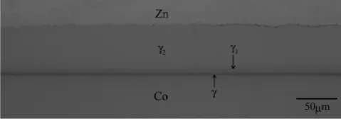
A typical cross-sectional DICOM image of the diffusion couple annealed at T = 573 K for t = 24 h (86.4 ks) is shown in Fig. 1. For this DICOM image in Fig. 1, the top and bottom regions are the Zn and Co specimens, respectively. As can be seen, layers with slightly different contrasts are formed at the original Co/Zn interface. To identify each layer, concentra-tion profiles of Co and Zn were measured by EPMA along the direction normal to the original interface. A result of the dif-fusion couple with T = 573 K and t = 30 h (108 ks) is indicat-ed in Fig. 2. In this figure, the ordinate and the abscissa show
the mol fraction yi of component i and the distance x
mea-sured from an arbitrary origin, respectively, and open circles and squares represent the mol fractions yCo and yZn,
respec-tively. As can be seen, the layers are the γ, γ1 and γ2 phases from the Co side to the Zn side. The thickness is much small-er for the γ and γ1 phases than for the γ2 phase. Similar results were obtained for all the diffusion couples annealed at T = 523–573 K. If we observe the edge of diffusion couple on the cross-section, we can find the location of the original Co/Zn interface. This observation indicates that the γ + γ1 + γ2 three-phase layer grows mainly into the Zn specimen but slightly towards the Co specimen.
According to a recent phase diagram in the binary Co–Zn system,25) the β
1 phase as well as the γ, γ1 and γ2 phases should appear as a stable compound phase at T = 523–573 K.
However, the β1 phase was not recognized in any annealed
diffusion couples in the present study. For reactive diffusion in binary alloy systems, the growth rate of a compound phase is predominantly determined by the interdiffusion coefficient and the solubility range of the growing phase.26–36) If the in-terdiffusion coefficient or the solubility range of a compound phase is small at an experimental annealing temperature, the compound phase cannot grow to visible thicknesses within realistic annealing times.26–36) At T = 523–573 K, the solubil-ity range is greater for the γ phase than for the β1, γ1 and γ2 phases, and close to one another among the β1, γ1 and γ2 phases.25) Consequently, the interdiffusion coefficient of the β1 phase must be much smaller than those of the γ, γ1 and γ2 phases. Furthermore, according to the result in Fig. 2, the in-terdiffusion coefficient has to be smaller for the γ phase than
Fig. 1 Cross-sectional DICOM image of diffusion couple annealed at T = 573 K for t = 24 h (86.4 ks).
[image:2.595.306.546.71.155.2] [image:2.595.324.527.213.408.2]for the γ1 phase but greater for the γ2 phase than for the γ1 phase.
3.2 Growth behavior of intermatellic layer
As shown in Fig. 1, a three-phase layer consisting of the γ,
γ1 and γ2 phases is formed at the original Co/Zn interface in the diffusion couple due to isothermal annealing at T = 523– 573 K. Hereafter, the three-phase layer is merely called the intermetallic layer. From DICOM images, such as that indi-cated in Fig. 1, the area Aj of the intermetallic layer
corre-sponding to the partial length wj of the original Co/Zn
inter-face was measured for cross-section j. The sums A and w were obtained by the equations23)
A= m
j=1
Aj (1a)
and
w= m
j=1
wj (1b)
from Aj and wj, respectively, where wj = 422 μm and m ≥ 5.
Using the values of A and w, the total thickness l of the inter-metallic layer was evaluated at each annealing time t as fol-lows:23)
l= A
w. (2)
The results for T = 523, 548 and 573 K are shown as open rhombuses, squares and circles, respectively, in Fig. 3. In this figure, the ordinate and the abscissa indicate the logarithms of
l and t, respectively. As can be seen, the thickness l monotoni-cally increases with increasing annealing time t. Furthermore, at T = 523–573 K, the experimental points for each annealing temperature lie well on a straight line. Consequently, l is ex-pressed as a power function of t as follows
l=k t t0
n
, (3)
where t0 is unit time, 1 s, which is adopted to make the
argu-ment t/t0 of the power function dimensionless. The
propor-tionality coefficient k has the same dimension as the thickness
l, and the exponent n is dimensionless. The dimensionless
argument of the power function is essentially important; oth-erwise the dimension of k varies depending on the value of n. From the experimental points in Fig. 3, k and n were evaluat-ed by the least-squares method as indicatevaluat-ed with various straight lines. The evaluated values of k and n are also shown in Fig. 3. According to the evaluation at T = 523–573 K, the overall growth rate of the intermetallic layer monotonically increases with increasing annealing temperature T.
According to Fig. 1, the interface between the γ2 and γ1 phases is rather distinguishable, but that between the γ1 and γ phases is almost invisible. From DICOM images, such as that shown in Fig. 1, the total thickness l1 of the γ + γ1 two-phase layer and the mean thickness l2 of the γ2 single-phase layer were evaluated using the relationships similar to eqs. (1a), (1b) and (2). Thus, there exists the following relationship among l1, l2 and l.
l=l1+l2 (4)
The results of l1, l2 and l for T = 573 K are shown as open rhombuses, squares and circles, respectively, in Fig. 4. In this figure, like Fig. 3, the ordinate and the abscissa indicate the logarithms of li and t, respectively. Since l1 is much smaller than l and l2, reliable measurement of l1 was possible only just at T = 573 K but not at T = 523–548 K. Even at T = 573 K, however, the open rhombuses in Fig. 4 are rather scattered due to small values of l1. In contrast, the open squares and circles are located well on each straight line. Therefore, we consider that li is expressed as a power function of t by the
following equation of the same formula as eq. (3).
li=ki tt
0
n
(5)
From the experimental points in Fig. 4, ki and n for li in eq. (5)
were evaluated by the least-squares method as shown with various straight lines. Since l1 and l2 are smaller than l, how-ever, the values of k1, k2 and n for l1 and l2 cannot be
estimat-Fig. 3 The total thickness l of the intermetallic layer versus the annealing time t at T = 523, 548 and 573 K shown as open rhombuses, squares and circles, respectively.
Fig. 4 The thicknesses l1, l2 and l versus the annealing time t shown as open
[image:3.595.69.279.520.752.2] [image:3.595.326.527.568.762.2]ed with the same reliability as those of k and n for l. Conse-quently, using the same value of n as l, k1 and k2 for l1 and l2 in eq. (5) were estimated from the open rhombuses and squares by the least-squares method as indicated with dotted and dashed lines, respectively. The values of n, k, k1 and k2 are shown in Fig. 4. As can be seen, k1 is smaller than k2 at T = 573 K. Although the identical value of n was adopted for l1, l2 and l, k1, k2 and k were independently evaluated from the cor-responding experimental points in Fig. 4 as mentioned earli-er. As a result, the relationship k = k1 + k2 does not necessarily hold, even though eq. (4) holds at each experimental anneal-ing time.
3.3 Rate-controlling process of intermetallic growth
The values of n in Fig. 3 are plotted against T as open cir-cles with error bars in Fig. 5. Here, the error bar shows the standard error. If the growth of the intermetallic layer is con-trolled by volume diffusion, n is equal to 0.5.26–36) On the other hand, n is equivalent to unity, if interface reaction gov-erns the layer growth.37–43) The temperature dependencies of the diffusion coefficient for the volume diffusion across the intermetallic layer and the interface reaction rate at the mov-ing interface of the intermetallic layer are schematically drawn as straight lines in Fig. 6. In this figure, the ordinates on the left-hand and right-hand sides show the logarithms of the diffusion coefficient and the interface reaction rate, re-spectively, and the abscissas on the top and bottom sides indi-cate the temperature T and the reciprocal of T, respectively. The temperature dependence of the diffusion coefficient is more remarkable than that of the interface reaction rate in Fig. 6(a), and vice versa in Fig. 6(b). Hereafter, as depicted in Fig. 6, the temperature range higher than A is called the high temperature range, and that lower than B is designated the low temperature range. On the other hand, the temperature range between A and B is denoted by the intermediate tem-perature range. If volume diffusion and interface reaction par-ticipate in the rate-controlling process for the layer growth, the relatively sluggish process governs the layer growth. In Fig. 6(a), interface reaction is much slower than volume dif-fusion in the high temperature range, and vice versa in the
low temperature range. In such a case, the layer growth is controlled by interface reaction in the high temperature range but by volume diffusion in the low temperature range. In the intermediate temperature range, however, both volume diffu-sion and interface reaction contribute to the rate-controlling process. Such a process is called a mixed rate-controlling pro-cess. The contribution of interface reaction increases with in-creasing temperature from B to A. In contrast, in Fig. 6(b), volume diffusion is much slower than interface reaction in the high temperature range, and vice versa in the low temperature range. In this case, the layer growth is governed by volume diffusion in the high temperature range but by interface reac-tion in the low temperature range. In the intermediate tem-perature range, the contribution of volume diffusion increases with increasing temperature from B to A.
According to the result in Fig. 5, n is close to 0.5 at T = 523–548 K, but takes a value of 0.85 at T = 573 K. As a con-sequence, volume diffusion predominantly controls the layer growth at T = 523–548 K, but interface reaction and volume diffusion contribute to the rate-controlling process at T = 573 K. The value n = 0.85 is closer to unity than to 0.5, and hence the contribution of interface reaction is more remark-able than that of volume diffusion. Such a mixed
[image:4.595.324.528.362.761.2] [image:4.595.69.270.572.772.2]trolling process of solid-state reactive diffusion was observed for various metal systems in previous studies.23,37–43) For the Co/Zn system, the contribution of interface reaction increas-es with increasing temperature from T = 523 K to T = 573 K according to the temperature dependence of the rate-con-trolling process in Fig. 6(a). This is the case also for the reac-tive diffusion in the Ni/Zn42) and Ag/Zn43) systems. On the other hand, the temperature dependence of the rate-con-trolling process in Fig. 6(b) was recognized for the reactive diffusion in the (Cu–Sn)/Nb system.37–39) As mentioned ear-lier, for the reactive diffusion in the Co/Zn system, the inter-metallic layer grows mainly into the Zn specimen and merely slightly towards the Co specimen. Therefore, the γ2/Zn inter-face is mobile, but the γ/Co interface is rather stationary. Consequently, it is plausible that the interface reaction at the mobile γ2/Zn interface dominantly influences the rate-con-trolling process of the layer growth at T = 573 K.
As can be seen in Fig. 3, n = 0.54–0.56 at T = 523–548 K, and n = 0.85 at T = 573 K. Since n is smaller for T = 523– 548 K than for T = 573 K, the dotted and dashed lines may intersect the solid line at very short annealing times. Accord-ing to a phase diagram in the binary Co–Zn system,25) howev-er, the phase relationship among the stable phases does not vary at T = 523–578 K. As a result, the growth rate of the in-termetallic layer should be a monotonical increasing function of the annealing temperature, and thus such intersection can-not be realized. In the early stages of reactive diffusion, the intermetallic layer is very thin, and hence the interdiffusion across the intermetallic layer occurs very fast. In this case, the interface reaction at the moving interface is the bottleneck for the layer growth, and the exponent becomes unity. As the an-nealing time increases, the layer thickness increases, and the interdiffusion slows down. In such a case, the interface reac-tion is no longer the bottleneck, and the exponent decreases from unity. Consequently, the transition of the rate-con-trolling process has to occur at an intermediate annealing time between the early and late stages. This type of transition was actually observed in previous studies.40,41)
3.4 Comparison with other results
The results for T = 523 and 573 K in Fig. 3 are represented as open circles with solid lines in Fig. 7(a) and 7(b), respec-tively. In contrast, as mentioned in Section 1, the reactive dif-fusion in the Co/Zn system was experimentally observed also by Duchenko et al.24) Unlike the present study, however, they
used a soldering technique to prepare Co/Zn diffusion
cou-ples. In their experiment, pure Co was soldered with pure Zn at T = 733–743 K for 30 s, and then cooled down to room temperature during 60 s. After cooling, the diffusion couple was annealed at temperatures of T = 523, 573, 623 and 673 K for various times up to 60 h (216 ks). At the original Co/Zn interface in the diffusion couple, an intermetallic layer com-posed of the γ, γ1 and γ2 phases was formed owing to solder-ing and annealsolder-ing. Accordsolder-ing to their result, the square of the total thickness l of the intermetallic layer is almost propor-tional to the annealing time t at T = 623 K. Such a relationship is called a parabolic relationship as mentioned earlier. On the other hand, at T = 523, 573 and 673 K, raw experimental re-sults of l are not reported in their article.24) Nevertheless, they mention that the parabolic relationship holds also at T = 523,
573 and 673 K. This means that the layer growth is mainly controlled by volume diffusion at T = 523–673 K. In their ar-ticle,24) the parabolic relationship is described as
l2=2Kt, (7)
and K = 2.7 × 10⁻¹⁵ and 1.4 × 10⁻¹⁴ m2/s are estimated for T = 523 and 573 K, respectively. Inserting these values of K into eq. (7), we obtain dashed lines in Fig. 7(a) and 7(b) for
T = 523 and 573 K, respectively. At T = 573 K in Fig. 7(b), l is close to each other between the solid and dashed lines with-in the experimental annealwith-ing times of the open circles, though n is smaller for the dashed line than for the solid line. In contrast, at T = 523 K in Fig. 7(a), l is greater for the dashed line than for the solid line, but n is not dissimilar to each oth-er between the solid and dashed lines. As mentioned above, pure Co was soldered with pure Zn at T = 733–743 K for 30 s in the experiment by Duchenko et al.24) Since the γ, γ
1 and γ2 phases are stable also at T = 733–743 K,25) they will be pro-duced by the reactive diffusion between solid-Co and mol-ten-Zn during soldering. The existence of these phases at the Co/Zn interface in the diffusion couple may influence
[image:5.595.326.526.68.459.2]quent growth of the intermetallic layer during annealing at
T = 523–673 K. On the other hand, a diffusion bonding
tech-nique was used to prepare the Zn/Co/Zn diffusion couple in the present study. In this technique,23) diffusion bonding is conducted at the same temperature as isothermal annealing, and thus formation and growth of the intermetallic layer oc-curs at the equivalent temperature. Such difference in the bonding technique may be the reason why l is greater for the dashed line than for the solid line in Fig. 7(a) and n is smaller for the dashed line than for the solid line in Fig. 7(b).
The solid-state reactive diffusion in the Cu/Zn system was experimentally observed in a previous study.44) In that exper-iment, Zn/Cu/Zn diffusion couples were also prepared by a diffusion bonding technique, and then isothermally annealed in the temperature range of T = 523–623 K for various times up to 49 h (176.4 ks). Owing to annealing, an intermetallic layer consisting of the γ and ε phases was formed at the orig-inal Cu/Zn interface in the diffusion couple, where the thick-ness is much smaller for the ε phase than for the γ phase. The total thickness of the intermetallic layer increases in propor-tion to a power funcpropor-tion of the annealing time. The exponent
n of the power function takes values of 0.60–0.62 at T = 523– 623 K. The values n = 0.60–0.62 indicate that volume diffu-sion predominantly controls the layer growth and interface reaction partially contributes to the rate-controlling process. The results for T = 523 and 573 K are represented as open squares with dashed lines in Fig. 8(a) and 8(b), respectively. In contrast, open circles with solid lines in Fig. 8(a) and 8(b) show again the results for T = 523 and 573 K in Fig. 3, re-spectively. As can be seen, the growth rate of the intermetallic layer is much smaller for the Co/Zn system than for the Cu/
Zn system. Therefore, Co works more effectively than Cu as a diffusion inhibitor against the reactive diffusion between UBM and the Zn phase in the eutectic Sn–Zn solder during solid-state heating under usual energization conditions.
4. Conclusions
The solid-state reactive diffusion in the Co/Zn system was
experimentally observed using the Zn/Co/Zn diffusion
cou-ples prepared by the diffusion bonding technique. The diffu-sion couples were isothermally annealed at temperatures of
T = 523, 548 and 573 K for various periods up to t = 211 h.
During annealing, an intermetallic layer composed of the γ,
γ1 and γ2 phases forms at the original Co/Zn interface in the diffusion couple, where the thickness is much smaller for the
γ and γ1 phases than for the γ2 phase. The total thickness of the three-phase layer is proportional to a power function of the annealing time. The exponent of the power function takes values of 0.54–0.56 at 523–548 K and that of 0.85 at 573 K under the present annealing conditions. This means that the layer growth is controlled mainly by volume diffusion at 523–548 K but by interface reaction and volume diffusion at 573 K.
Acknowledgements
The present study was supported by the Iketani Science and Technology Foundation in Japan. The study was also par-tially supported by a Grant-in-Aid for Scientific Research from the Ministry of Education, Culture, Sports, Science and Technology of Japan.
REFERENCES
1) T.B. Massalski, H. Okamoto, P.R. Subramanian and L. Kacprzak:
Bina-ry Alloy Phase Diagrams, vol. 3 (ASM International, Materials Park, OH, 1990) p. 3417.
2) K. Suganuma and K. Niihara: J. Mater. Res. 13 (1998) 2859–2865.
3) S.-P. Yu, H.-J. Lin, M.-H. Hon and M.-C. Wang: J. Mater. Sci.: Mater. Electron. 11 (2000) 461–471.
4) I. Shohji, T. Nakamura, F. Mori and S. Fujiuchi: Mater. Trans. 43 (2002) 1797–1801.
5) M. Date and K.N. Tu: J. Mater. Res. 19 (2004) 2887–2896.
6) M.N. Islam, Y.C. Chan, M.J. Rizvi and W. Jillek: J. Alloy. Compd. 400 (2005) 136–144.
7) J.-W. Yoon and S.-B. Jung: J. Mater. Res. 21 (2006) 1590–1599.
8) K. Suganuma and K.-S. Kim: J. Mater. Sci.: Mater. Electron. 18 (2007) 121–127.
9) K. Tanida, M. Umemoto, Y. Tomita, M. Tago, R. Kajiwara, Y. Akiyama and K. Takahashi: Jpn. J. Appl. Phys. 42 (2003) 2198–2203.
10) K. Tanida, M. Umemoto, N. Tanaka, Y. Tomita and K. Takahashi: Jpn. J. Appl. Phys. 43 (2004) 2264–2270.
11) R. Labie: Dr. Thesis, Katholieke Universiteit Leuven, Leuven, (2007). Fig. 8 The total thickness l of the intermetallic layer versus the annealing
time t for the Co/Zn system shown as open circles with solid lines: (a) 523 K; and (b) 573 K. The corresponding results for the Cu/Zn system reported in a previous study44) are indicated as open squares with dashed
[image:6.595.68.270.343.732.2]12) A. La Manna, T. Buisson, M. Detalle, K.J. Rebibis, D. Velenis, W. Zhang and E. Beyne: Proc. 62nd Electronic Components and Technol-ogy Conference, San Diego, (2012) 532.
13) W. Zhang, Z. Mai, L. Bogaerts, M. Gonzalez, G. Vakanas, A. La Manna and E. Beyne: Proc. 4th Electronic System-Integration Technology Conference, Amsterdam, (2012) 1.
14) R. Labie, E. Beyne and P. Ratchev: Proc. 5th Electronics Packaging Technology, Singapore, (2003) 584.
15) R. Labie, P. Ratchev and E. Beyne: Proc. 55th Electronic Components and Technology Conference, Lake Buena Vista, (2005) 449.
16) S. Kim and J. Yu: Proc. Electronic Materials and Packaging, Taipei, (2008) 313.
17) C. Wang and S. Chen: Intermetallics 16 (2008) 524–530.
18) G. Humpston: J. Mater. Sci.: Mater. Electron. 21 (2010) 584–588.
19) C. Wang and C. Kuo: Mater. Chem. Phys. 130 (2011) 651–656.
20) W. Zhang, A. La Manna, P. Soussan and E. Beyne: Proc. 3rd IEEE Int. Workshop on Low Temperature Bonding for 3D Integration, Tokyo, (2012) 65.
21) Y. Liang, W. Tsao, C. Chen, D. Yao, A. Huang and Y. Lai: J. Appl. Phys. 111 (2012) 043705, 1–7.
22) C. Wang, C. Kuo, S. Huang and P. Li: Intermetallics 32 (2013) 57–63.
23) M. O, Y. Takamatsu and M. Kajihara: Mater. Trans. 55 (2014) 1058– 1064.
24) O.V. Duchenko, V.M. Vereshchaka and V.I. Dybkov: J. Alloy. Compd. 288 (1999) 164–169.
25) T.B. Massalski, H. Okamoto, P.R. Subramanian and L. Kacprzak:
Bina-ry Alloy Phase Diagrams, vol. 2 (ASM International, Materials Park, OH, 1990) p. 1263.
26) M. Kajihara: Acta Mater. 52 (2004) 1193–1200.
27) M. Kajihara: Mater. Sci. Eng. A 403 (2005) 234–240.
28) M. Kajihara: Mater. Trans. 46 (2005) 2142–2149.
29) M. Kajihara: Diffus. Defect Forum 249 (2006) 91–96. 30) M. Kajihara: Mater. Trans. 47 (2006) 1480–1484.
31) Y. Tanaka and M. Kajihara: Mater. Trans. 47 (2006) 2480–2488.
32) M. Kajihara and T. Yamashina: J. Mater. Sci. 42 (2007) 2432–2442.
33) M. Kajihara: Mater. Trans. 49 (2008) 715–722.
34) M. Kajihara: J. Mater. Sci. 44 (2009) 2109–2118.
35) M. Kajihara: Mater. Trans. 51 (2010) 1242–1248.
36) M. Kajihara: Mater. Trans. 53 (2012) 1896–1904.
37) Y. Muranishi and M. Kajihara: Mater. Sci. Eng. A 404 (2005) 33–41.
38) T. Hayase and M. Kajihara: Mater. Sci. Eng. A 433 (2006) 83–89.
39) K. Mikami and M. Kajihara: J. Mater. Sci. 42 (2007) 8178–8188.
40) M. Kajihara and Y. Tejima: J. Phys.: Conf. Ser. 165 (2009) 012091, 1–4.
41) Y. Tejima, S. Nakamura and M. Kajihara: J. Mater. Sci. 45 (2010) 919– 928.
42) H. Sakaguchi and M. Kajihara: Abst. Autumn Meeting Jpn. Inst. Met. (2014) 229.
43) H. Sakaguchi, M. O, N. Nakada and M. Kajihara: Abst. Autumn Meet-ing Jpn. Inst. Met. (2016) 318.