Effect of Zinc Addition on Void Formation in Solid-Liquid Interdiffusion Bonding
of Copper
S. Fukumoto
1, T. Miyazaki
2, M. Matsushima
1and K. Fujimoto
11Graduate School of Engineering, Osaka University, 2–1 Yamadaoka, Suita, Osaka 565–0871, Japan 2Graduate Student of Osaka University, 2–1 Yamadaoka, Suita, Osaka 565–0871, Japan
Solid–liquid interdiffusion bonding of Cu was carried out at 573 K with deposited Sn and Cu films. The effect of Zn addition to the faying surfaces was investigated to reduce Kirkendall voids. At the beginning of the reaction, molten Sn reacted with Cu to form Cu6Sn5, and Cu3Sn successively formed between the Cu6Sn5 and the Cu. Many voids formed in the Cu3Sn phase, especially close to the Cu3Sn/Cu interface. When Zn was added in the faying surfaces, Zn was segregated near the interface of Cu/Cu3Sn and the grain boundaries of Cu3Sn. The Zn segregation inhibited diffusion of Cu due to the effect of solute drag, which also delayed growth of the Cu3Sn layer. As a result, the fluxes of Cu and Sn via the Cu3Sn phase were balanced out, which reduced the Kirkendall void formation. [doi:10.2320/matertrans.MD201509]
(Received December 5, 2015; Accepted February 2, 2016; Published March 18, 2016)
Keywords: Micro-joining, Diffusion bonding, Interdiffusion, Intermetallic compound, Kirkendall void, Zinc
1. Introduction
Power devices are widely used as key technologies for power and railway systems. These power devices rely on bonds such as chip/Cu substrate (die bonding) and wire-lead/
chip bonds, which have historically used Sn-based lead-free solders.
SiC and GaN are expected to be used as next-generation power semiconductors because they exhibit better efficiency and can operate at higher temperatures than Si chips. With junction temperatures approaching 473 K with SiC and GaN semiconductors, standard Sn-based lead-free solders cannot be applied for die bonding. To address the problems associat-ed with the use of standard Sn-basassociat-ed lead-free solders at higher temperatures, solid–liquid interdiffusion bonding is a possible alternative for the die bonding process. In solid–liq-uid interdiffusion bonding, metals with low melting points such as Sn and In are sandwiched between copper bases and heated above the melting point of the inserted materials to realize die bonding by solid–liquid reaction diffusion.1–6) The liquid phase then reacts with the base copper to form a bond layer of intermetallic compounds (IMCs) that exhibits a high-er melting point than the melting point of the inshigh-erted mathigh-eri- materi-al.
In solid–liquid interdiffusion bonding in a Cu–Sn system, the final bond layer is composed of Cu3Sn. However, voids are frequently observed near the Cu3Sn/Cu interface and at the interface between the Sn-based solder and the Cu sub-strate. When the molten Sn-based solder alloy wets the cop-per, Cu6Sn5 and Cu3Sn IMCs form at the solder/Cu interface. In most cases, voids also form at the Cu3Sn/Cu interface and/
or in Cu3Sn.7–9) Both the growth of IMCs and void formation affect the solder joint reliability, which can degrade the me-chanical and electrical properties of the joints. It has been reported that the mechanism of void formation in the Cu/Sn system is basically caused by unbalanced diffusion fluxes (Cuflux > Snflux) in the Cu3Sn phase, that is to say, the Kirken-dall effect.10) Since Kirkendall voids are formed due to unbal-anced diffusion fluxes, tiny amounts of additive elements will affect void formation and the growth of IMCs. Thus, the
ef-fects of various kinds of additive elements on the growth be-havior of IMCs have been reported. For example, the addition of Ni was reported to reduce the growth of the Cu3Sn lay-er.11,12) Ma et al. reported that the addition of 0.05 mass% of La also reduced the growth of Cu6Sn5.13) Above all, the addi-tion of a small amount of Zn is significantly effective for sup-pressing the growth of Cu6Sn5 and Cu3Sn and the formation of voids in the soldering process using Sn-based solders.14,15) The growth of IMCs and the formation of voids were also suppressed between the Sn–Ag solder and the Cu–Zn alloy substrate due to the segregation of Zn at the Cu6Sn5/CuZn interface.16)
In the present study, a small amount of Zn was added to the faying surface in the solid–liquid interdiffusion bonding of Cu using a Sn thin-film filler metal to reduce void formation. Metallurgical examination was carried out to investigate the effect of Zn on the solid–liquid interdiffusion bonding.
2. Experimental procedures
The materials used were oxygen-free Cu rods 3 mm and 5 mm in diameter whose faying surfaces were polished with #4000-grit emery paper. They were then pickled in a 5% HCl solution and rinsed in ethanol. The designs of the faying in-terfaces and the bonding setup are shown in Table 1 and Fig. 1. The faying surface of Cu was coated with Sn, Cu, and/
[image:1.595.306.551.698.787.2]or Zn in order by vapor deposition in accordance with Table 1 by resistance heating under an atmosphere of 5 × 10⁻³ Pa. The faying surface of Design-A had only a 4-μm-thick Sn
Table 1 Designs of faying interfaces produced by vapor deposition coating.
Thickness (μm)
Sn Cu Zn Sn
Design-A 4 - -
-Design-B1 2 0.38 - 2
Design-B2 2 0.63 - 2
Design-C1 2 0.38 0.02 2
Design-C2 2 0.63 0.02 2
Materials Transactions, Vol. 57, No. 6 (2016) pp. 846 to 852
layer. A Cu thin film was deposited between the Sn films as an intermediate layer to fabricate a Sn/Cu/Sn faying surface, that is, Design-B. The thicknesses of the intermediate Cu lay-ers in Design-B were 0.38 μm and 0.63 μm, denoted as De-sign-B1 and B2, respectively. Similarly, a 0.02-μm-thick Zn layer was deposited between the Sn and Cu layers on the De-sign-B1 and B2 faying surfaces, denoted as Design-C1 and
C2 faying surfaces, respectively. The bonding between the
ϕ3 mm and ϕ5 mm Cu specimens was performed at 573 K for bond times of 300, 600, and 1800 s under a bonding pressure of 10 MPa in nitrogen gas flow atmosphere (2 L/min), as shown in Fig. 1b. The microstructures of the bond layers were observed by scanning electron microscopy (SEM) and trans-mission electron microscopy (TEM) with energy dispersive X-ray spectroscopy (EDX). The specimens for TEM observa-tion were prepared by the focused ion beam (FIB) method.
3. Results and discussion
3.1 Bonding using mono-Sn film
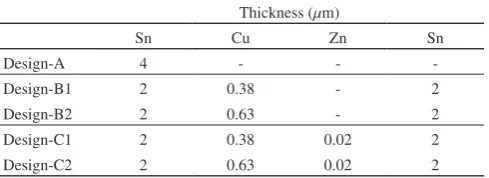
The copper was bonded to itself using a mono-Sn film, that is, the Design-A faying surface, at 573 K. The cross sections Fig. 2 Growth of IMC bond layers using deposited Sn coating (Design-A) at bonding times of (a) 300, (b) 600, and (c)1800 s. Bonding temperature is 573 K.
Fig. 1 (a1)–(a3) Designed faying surfaces prepared by vapor deposition coating and (b) set-up of solid–liquid diffusion bonding of copper. Details of the layered structures are shown in Table 1.
[image:2.595.48.296.63.647.2] [image:2.595.322.531.69.546.2]of the bonded layers are shown in Fig. 2. When the tempera-ture reaches 505 K, Sn melts, which improves the adhesion between the two materials. Once a liquid phase formed, Cu dissolved into the liquid Sn, resulting in the formation of Cu6Sn5. Subsequently, Cu3Sn formed at the interface between Cu6Sn5 and Cu due to reaction diffusion during the heating process up to 573 K (Fig. 2a). Because the amount of liquid Sn was quite small, it was consumed completely to form Cu– Sn IMCs immediately. The thickness of the Cu3Sn layer in-creased with decreasing Cu6Sn5 thickness during the holding process at 573 K, until the whole bond layer was occupied by Cu3Sn (Fig. 2c). It is worth noting that many voids appeared in the bond layer and at the interface of Cu3Sn/Cu as the thickness of the Cu3Sn layer increased. In a Cu3Sn phase, dif-fusion rate of Cu is faster than that of Sn as a result of the
so-called ordered Cu3Au rule. In general, in compounds of the form AmBn, where m/n is greater than 2, the atoms of species A diffuse considerably faster than those of species B. d Heurle et al. explained the phenomenon by the fact that, in general, the majority atoms constitute a continuous network in which a vacancy can easily migrate. On the other hand, the motion of minority atoms requires either the coexistence of two vacancies (minority and majority) or a local destruction of the crystalline lattice.17,18) Therefore, the majority atoms of Cu are more mobile than the minority atoms of Sn in Cu3Sn. In the present study, Cu3Sn grew between Cu and Cu6Sn5 due to solid-phase reaction diffusion. Thus, most of these voids are believed to be Kirkendall voids.
[image:3.595.84.517.68.554.2]3.2 Bonding using Cu/Sn films
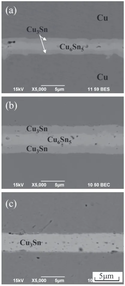
In the case of a mono-Sn film, Cu atoms were supplied from only Cu base metals to form Cu3Sn. Then, a Cu thin film was supplied between the two Sn thin films of the faying sur-face (Fig. 1, Design-B) to shorten the apparent reaction time to form a Cu3Sn layer. These Cu films are expected to work as another source of Cu to form Cu3Sn. Figure 3 shows the cross sections of the bond interfaces of Cu bonded using Design-B1 and Design-B2 faying surfaces at 573 K with bond times of 300, 600, and 1800 s. Cu6Sn5 disappeared at the bond time of 600 s when using both Design-B1 and Design-B2 faying sur-faces. Even at 300 s of bond time, most of the bond layer was composed of Cu3Sn as a result of the increasing thickness of the intermediate Cu film (Fig. 3d). By locating a thin Cu film in the deposited layer as an intermediate supply source, the transformation from Cu6Sn5 to Cu3Sn was completed in a
shorter time than in the case of bonding using only the mo-no-Sn film as the faying surface. However, the unbalanced diffusion flux between Sn and Cu in the Cu3Sn phase has not been solved, and the addition of a Cu film into the Sn films increased the number of Cu/Sn interfaces. As a result, many more Kirkendall voids formed in the resulting bond layer than occurred using the mono-Sn film.
3.3 Effect of zinc
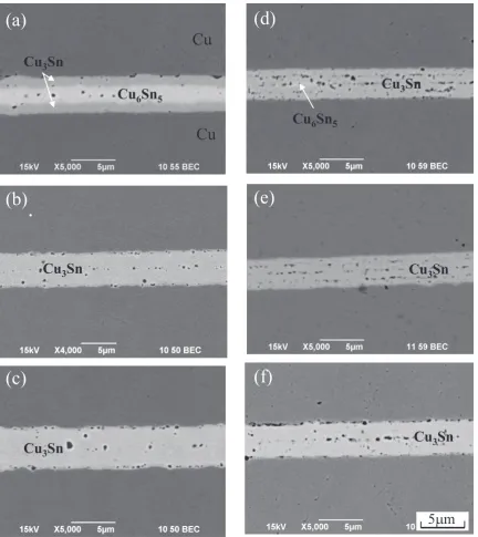
The addition of a deposited Cu film into the deposited Sn film shortened the apparent bond time; however, it increased the number of Kirkendall voids. Zn was therefore deposited between the deposited Cu/Sn films. Figure 4 shows the cross sections of the bond interfaces of Cu bonded using the De-sign-C1 and Design-C2 faying surfaces at 573 K with bond times of 300, 600, and 1800 s. The microstructure of the bond Fig. 4 Effect of Zn addition on IMC growth as a function of bond times of (a) 300, (b) 600, and (c) 1800 s for the Design-C1 faying surface and of (d) 300,
(e) 600, and (f) 1800 s for the Design-C2 faying surface. Bonding temperature is 573 K.
[image:4.595.85.513.65.546.2]layer composed of Cu3Sn and Cu6Sn5 was similar to that of the bond layer without Zn. However, the number of Kirkend-all voids drasticKirkend-ally decreased by the addition of Zn. On the other hand, it took longer for the whole bond layer to show only a Cu3Sn phase than was the case with bonding without Zn. When Zn was added in the faying surface of Design-B1, Cu6Sn5 remained in the bond layer even at the bond time of 600 s (see Fig. 4b). In a similar fashion, Cu6Sn5 layers were obviously observed in the bond layer for the bond time of 300 s when Zn was added in the faying surface of Design-B2 (see Fig. 4d).
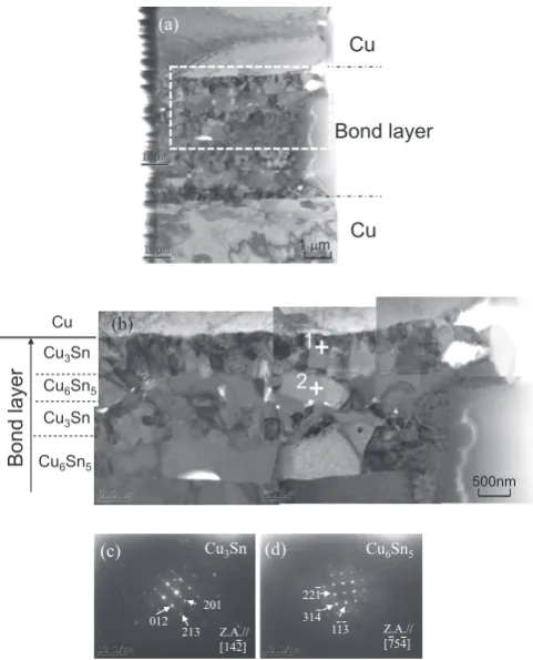
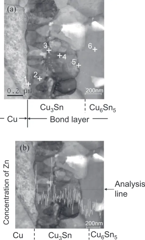
The distribution of Zn was investigated by SEM with EDX analysis. Figure 5 shows the Zn distribution in the bond layer using the faying surface with the addition of Zn. Zn was mainly segregated at the interface between the bond layer and the base metal, and some Zn remained around the voids locat-ed at the center of the bond layer. These voids were not Kirkendall voids since they were relatively-large compared with the voids that were formed at the Cu/bond layer inter-face. They were probably formed when the final liquid phase were solidified isothermally at the center of bond layer. The detailed microstructures of the bond layers with a bond time of 300 s were observed using TEM with EDX analyses (Fig. 6 and Fig. 7). Table 2 shows the results of quantitative EDX
analysis at each point shown in Fig. 7a. The beam diameter used for EDX analysis was ~2 nm. TEM observation revealed that the bond layer was composed of a Cu6Sn5/Cu3Sn layered microstructure, and the grain size of Cu3Sn was finer than that of Cu6Sn5. Such obvious layered structure were not observed by SEM as shown in Fig. 4a. Because the layered structure is transition state, and the thickness of vapor deposition coating was not controlled perfectly. Therefore, some degree of vari-ability on microstructures could occur even at the same bond-ing condition. Analysis points Nos. 1–5 in Fig. 7 correspond to Cu3Sn and No. 6 corresponds to Cu6Sn5. The EDX points and line analyses revealed that Zn was segregated at the inter-face between Cu3Sn and the Cu base metal and at the grain boundary of Cu3Sn.
Figure 8 shows the TEM bright-field images and selected area diffraction patterns (SADPs) of the IMC layer bonded for 1800 s. When the bond time reached 1800 s, most of the bond layer was composed of coarse grains, and there were fine grains near the interface between the bond layer and the Cu base metal. Cu6Sn5 completely disappeared in the bond layer. It is particularly worth noting that Cu3Sn with fine grains formed next to the interface between the bond layer and the Cu base metal. As shown in Fig. 5, the fine grain area corresponds to where Zn was segregated. The grain boundary segregation of the solute inhibits the mobility of the grain boundary, that is to say, solute drag, which delays the grain growth of Cu3Sn next to the Cu base metal. The interfacial and grain boundary segregation of Zn also inhibits diffusion of Cu in Cu3Sn. The atoms of Sn are also affected by the seg-Fig. 5 (a) SEM image and (b) Zn mapping of the distribution of Zn in the
bond interface bonded for 1800 s using the Design-C1 faying surface. Bonding temperature is 573 K.
Fig. 6 TEM observation of IMC layer bonded for 300 s with the Design-C1 faying surface. (a) Bright-field image of IMC layer, (b) highlighted area in (a), (c) SADP from point 1, and (d) SADP from point 2. Bonding tem-perature is 573 K.
[image:5.595.307.548.68.366.2] [image:5.595.77.259.68.432.2]regation of Zn. However, because Sn is the minor atom for diffusion, as mentioned above, the effect of Zn segregation on the mobility of Sn in the Cu3Sn phase might be limited. As a result, the formation of Kirkendall voids is inhibited by the addition of Zn.
4. Conclusions
Copper was bonded to itself by using a deposited Sn film
including Cu and/or Zn. The effect of Zn addition on the growth rate of the intermetallic compounds and the formation of Kirkendall voids was investigated. The following results were obtained:
(1) When Cu was bonded at 573 K using the faying surface of the deposited Sn film, liquid Sn immediately reacted with Cu to form Cu6Sn5. Cu3Sn formed successively between Cu6Sn5 and Cu, and the thickness of the Cu3Sn layer in-creased with increasing bond time. Many voids formed near the interface between Cu3Sn and the Cu base metal with in-creasing thickness of the Cu3Sn phase. Finally, the bond layer consisted of only single-phase Cu3Sn.
(2) The time needed to form single-phase Cu3Sn in the bond layer was shortened by using Sn/Cu/Sn multilayered films. A thin Cu layer on the faying surface worked as an in-termediate supply source to form Cu3Sn. On the other hand, the number of Kirkendall voids increased at the Cu/Cu3Sn interface in the bond layer.
(3) The number of Kirkendall voids decreased by the addi-tion of a small amount of Zn in the faying surface. The segre-gation of Zn at the Cu3Sn/Cu interface and Cu3Sn grain boundaries inhibited the mobility of Cu. On the other hand, the addition of Zn reduced the growth rate of the Cu3Sn layer.
Acknowledgements
The authors gratefully thank Dr. Makoto Takahashi for his experimental support. This work was partially supported by JSPS KAKENHI Grand Numbers 24560883, 25289242, and the New Energy and Industrial Technology Development Or-ganization (NEDO).
REFERENCES
1) T. Fujimoto, S. Fukumoto, T. Miyazaki, Y. Kashiba, K. Shiotani and K. Fujimoto: J. Phys. Conf. Ser. 379 (2012) 012026.
2) J.F. Li, P.A. Agyakwa and C.M. Johnson: Acta Mater. 59 (2011) 1198– 1211.
3) S. Bader, W. Gust and H. Hieber: Acta Metall. Mater. 43 (1995) 329– 337.
[image:6.595.309.547.72.241.2]4) C.C. Lee and Y.-C. Chen: Thin Solid Films 286 (1996) 213–218. 5) S. Fukumoto, K. Miyake, S. Tatara, M. Matsushima and K. Fujimoto: Table 2 Results of quantitative EDX analysis at each point shown in Fig. 7.
Point Composition (at%)
Cu Sn Zn
1 92.9 5.2 1.9
2 75.7 24.0 0.3
3 72.2 23.4 4.4
4 74.5 35.4 0.1
5 69.5 30.1 0.4
6 54.7 45.1 0.2
Fig. 8 TEM observation of IMC layer bonded for 1800 s with the De-sign-C1 faying surface. (a) Bright-field image, (b) SADP from point 1, and (c) SADP from point 2. Bonding temperature is 573 K.
Fig. 7 (a) TEM bright-field image and (b) EDX analysis of Zn near Cu/ Cu3Sn bond interface. The bonding was carried out for 300 s using the Design-C1 faying surface. The compositions at each point in (a) are shown in Table 2. Bonding temperature is 573 K.
[image:6.595.51.289.73.466.2] [image:6.595.46.291.551.653.2]Mater. Trans. 56 (2015) 1019–1024.
6) P.J. Wang, J.S. Kim and C.C. Lee: J. Electron. Mater. 38 (2009) 2106– 2111.
7) W. Yang, R.W. Messler, Jr. and L.E. Felton: J. Electron. Mater. 23 (1994) 765–772.
8) J.Y. Kim and Jin Yu: Appl. Phys. Lett. 92 (2008) 092109.
9) T.S. Huang, H.W. Tseng, Y.H. Hsiao, C.H. Cheng, C.T. Lu and C.Y. Liu: Electrochem. Solid-State Lett. 14 (2011) H393–H396.
10) M.Y. Tsai, S.C. Yang, Y.W. Wang and C.R. Kao: J. Alloy. Compd. 494 (2010) 123–127.
11) T. Laurila, J. Hurtig, V. Vuorine and J.K. Kivilahti: Microelectron.
Re-liab. 49 (2009) 242–247.
12) V. Vuorinen, T. Laurila, T. Mattila, E. Heikinheimo and J.K. Kivilahti: J. Electron. Mater. 36 (2007) 1355–1362.
13) X. Ma, Y. Qian and F. Yoshida: J. Alloy. Compd. 334 (2002) 224–227. 14) C.-Y. Yu and J.-G. Duh: Scr. Mater. 65 (2011) 783–786.
15) J.Y. Kim, J. Yu and S.H. Kim: Acta Mater. 57 (2009) 5001–5012. 16) H.F. Zou, Q.K. Zhang and Z.F. Zhang: J. Electron. Mater. 40 (2011)
1542–1548.
17) F.M. d Heurle and P. Gas: J. Mater. Res. 1 (1986) 205–221.
18) F.M. d Heurle, P. Gas, C. Lavoie and J. Philibert: Z. Metallk. 95 (2004) 852–859.