Flip Chip Bump Formation of Sn–1.8Bi–0.8Cu–0.6In Solder by Stencil Printing
Jaesik Lee
1, Jae-Pil Jung
2, Chu-Seon Cheon
3, Yunhong Zhou
1and Michael Mayer
1 1Dept. of Mechanical Engineering, University of Waterloo, Waterloo, Ontario, N2L 3G1, Canada2Dept. of Materials Science and Engineering, University of Seoul, Seoul, 130-743, Korea 3
Danyang Soltec Co. Ltd., Hwaseong-si, Gyeonggi-do, 445-861, Korea
Flip chip bumping by stencil printing method using a new composition of solder paste, Sn–1.8%Bi–0.8%Cu–0.6%In, all in mass%, was investigated. Sn–3.5%Ag, Sn–37%Pb and Sn–36%Pb–2%Ag were selected as references for the experiment. The solder pastes were printed on the under bump metallization (UBM) of a Si-wafer using a stencil, where diameter and thickness of the stencil opening were 400 and 150mm, respectively. The UBM deposit comprised 0.4mmeach of Al, Ni and Cu, and 20 nm of Au from bottom to top of the metallization, sequentially. The printed paste bumps were reflow soldered in air, and the peak soldering temperature of Sn–1.7Bi–0.8Cu–0.6In and Sn–3.5Ag was 523 K and of Sn–37Pb and Sn–36Pb–2Ag was 503 K. From the experimental results the solder bumps of Sn–1.8Bi–0.8Cu–0.6In alloys were well-formed with a mean height of 260mm. The shear strength of Sn–1.8Bi–0.8Cu–0.6In at 523 K (as-reflowed) showed the highest value of 6.5N followed by those of Sn–3.5Ag, Sn–37Pb and Sn–36Pb–2Ag solders. After 1000 h aging, while the shear strength of the Sn–1.8Bi–0.8Cu–0.6In showed 27% decrease compared to as-reflowed conditions, it was still 15–30% higher than those of Sn–37Pb, Sn–36Pb–2Ag and Sn–3.5Ag solders. Intermetallic compounds (IMCs) formed on the interface between solder and UBM were (Cu,Ni)6Sn5. As aging time went on up to 1000 h, the
content of Ni in the IMC changed from 6.6% at initial stage (as-reflowed) to 13.5% at final stage (1000 h aging).
(Received May 19, 2005; Accepted August 30, 2005; Published November 15, 2005)
Keywords: tin–1.8 bismuth–0.8 copper–0.6 indium solder, lead-free solder, shear strength, solder paste and microstructure
1. Introduction
Flip chip packaging technology1,2)which was developed at IBM in 1960s was aimed at reducing package size and increasing the electric characteristics of microelectronic devices. Fabrication of metal bumps on the chip is important for the flip chip because it affects the number of I/O counts in a fine pitched device and the reliability of the device. Several methods of bumping technology have been introduced such as vapor deposition, solder ball, electro-deposition and stencil printing. Among them, vapor-deposition method was employed at IBM in 1960. But this technology had several disadvantages. It was hard to bump on a big sized wafer, too expensive, and difficult to apply because it needed to be deposited in vacuum.3)Due to those disadvantages, the stencil printing and electroplating methods have been mainly used in wafer level packaging up to the present. As the stencil printing method has the benefit of reducing the price of the big pitched-devices, it has been the subject of many researches.4) Other advantages of employing a stencil printing method for wafer level packaging are its compati-bility with the conventional reflow machine and new solder materials, the composition of which can vary in a wide range. Recently, the demands for replacing the Sn–37 mass%Pb (hereafter mass% will be omitted) with Pb-free solders has sharply increased in Europe, Japan and the United States due to the toxicity of Lead (Pb) to environment and human body.5,6)Although many Pb-free solders have been proposed, there are no obvious replacements for the Sn–37Pb which is most common in electronics. Many Pb-free solders such as Sn–Ag–Cu, Sn–Ag, and Sn–Ag–Bi have been in use for years. Among them, the Sn–(3.0–4.0)Ag–(0.5–0.75)Cu sol-ders and Sn–0.7Cu solder have been considered as the most popular candidates for reflow soldering and for wave soldering, respectively. However, none of those Pb-free solders can perfectly replace the Sn–37Pb in all applications. Furthermore, taking costs of raw material into consideration,
most of the Pb-free solders are three times more expensive than Pb solder. Therefore a new solder which is relatively cheap and overcomes the shortcommings of those solders needs to be developed.
It has been known that adding a small amount of Bi into the solder improves the wettability while decreasing the solidus temperature.7) Shohji et al.8) also reported that the tensile strength of Sn–3Ag–2Bi solder was higher than that of other lead-free solders, Sn–3.5Ag and Sn–3.5Ag–0.75Cu, and was higher by approximately 1.4 times than that of Sn–37Pb, over the temperature range from 233 to 393 K. Many studies have been conducted to optimize the amount of Bi, which affectes the solder joint reliability. The recent result by Hwang and Suganuma9)showed that solders including Bi up to 3% were not detrimental to the solder joint. Another effort, adding In into the solder, was made to reduce the brittleness of Bi.
In this work, Sn–1.8Bi–0.8Cu–0.6In solder, which is based on relatively inexpensive Sn–Cu solder, was developed to bypass some disadvantages of the Sn–(3.0–4.0)Ag–(0.5–0.7) Cu solders and Sn–0.7Cu solder. These new solders might have many benefits for electronic applications. However, not enough reliable data has been reported compared to the conventional solders.10)
The purposes of this study are to evaluate the bump formation and reliability of this new solder paste composed of Sn–1.8Bi–0.8Cu–0.6In. The powder particle size, printing accuracy, and bump formed after soldering at 523 K were observed by scanning electron microscopy (SEM). Exper-imental shear strengths and the microstructures of the Sn– 1.8Bi–0.8Cu–0.6In solder were compared to those of Sn– 37Pb, Sn–36Pb–2Ag, and Sn–3.5Ag solders after various aging times to investigate the solder joint reliability.
2. Experimental Procedure
each of Al, Ni and Cu, and 20 nm of Au from bottom to top of the metallization, sequentially (Fig. 1). Al, Ni and Cu layers were deposited by thermal evaporation, and then Au was deposited as a wetting layer by E-gun evaporation. Finally, a Ti layer with thickness of 50 nm for use as a solder dam against spreading of the molten solder was deposited over the Au-layer by E-gun evaporation.
Sn–1.8Bi–0.8Cu–0.6In solder was stencil printed on the UBM by a semi-automatic paste printer. The diameter and thickness of the stencil opening were 400 and 150mm, respectively. After stencil printing, reflow soldering in air was employed. The preheating temperature was 423 K. The peak soldering temperature of Sn–1.7Bi–0.8Cu–0.6In and Sn–3.5Ag was 523 K, and that of Sn–37Pb and Sn–36Pb– 2Ag was set to 503 K. The reflow soldering profile is as shown in Fig. 2.
Bump shapes after reflow soldering were observed. To investigate the reliability of the bumping procedure, the microstructure and the shear strength of the solder bumps were evaluated after various aging times. The soldered bumps were aged by isothermal treatment at 423 K for 0, 300, 500, and 1000 h. The shear strength of the solder bumps was measured by a PTR-1000 shear test machine. A total of 20 bumps under the same conditions were sheared, the measured strength values were averaged, and the result is given as shear strength in this work. The moving rate of the shearing tip was 200mm/s, and the clearance between the shearing tip and the Si-substrate was 10mm.
To observe the IMC along the bonded interface, the samples polished up to 0.04mm were etched and the bulk solder was removed. A scanning electron microscope con-nected to an energy dispersive spectrometor (EDS) was employed to examine the IMC layers on the solder/UBM interface of cross-sectioned samples and the fracture surfaces after shear test.
3. Results and Discussion
3.1 The bump formation of Sn–1.8Bi–0.8Cu–0.6In paste solder
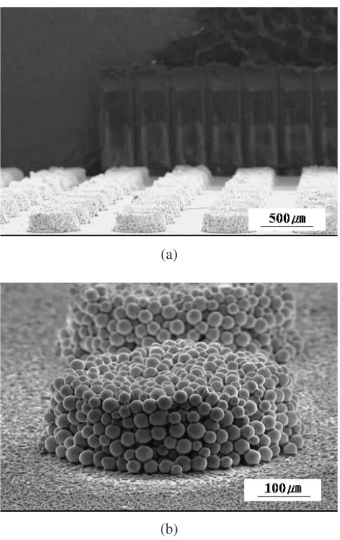
Prior to evaluating the mechanical characteristics of Sn– Bi–Cu–In solder, the shape of paste powder and bumps formed after soldering at 523 K was observed by SEM. Figures 3(a) and (b) show parts of the specimen printed with Si–1.8Bi–0.8Cu–0.6In solder paste. It was heated at 373 K for 1 h to allow evaporation of the flux and to be suitable for SEM observation. The paste solder was relatively uniformly stencil-printed on the UBM and exhibited good rolling behavior, filling efficiency, and printing results. The powder particle size ranged from 19 to 36mm, and the height of stencil printed powder was 144mm.
The bump shapes of Sn–1.7Bi–0.8Cu–0.6In paste solder after one reflow cycle at 523 K are shown in Fig. 4(a). Crater-shaped holes were observed at the top and side of the bump. Generally, the solder pastes include flux or solvent ranging from 35 to 60 vol%, and gas is formed by flux evaporation during heating the paste solder.11) This gas went out of the paste solder by buoyancy in the process of heating and melting.12)Chanet al.13)suggested that the buoyancy force Solder bump
substrate
N UBM
Solder dam Solder bump
substrate
Ti(50nm) Au(20nm) Cu(400nm) Ni(400nm) Al(400nm)
Fig. 1 Schematic of solder bump on UBM of Si-wafer.
200 400 600
0 100 200 300 400
Time, t/s
T
emperatur
e,
T
/
K Preheating zone Reflow zone
Fig. 2 Schematic diagram of reflow profile.
(a)
(b)
[image:2.595.306.548.68.452.2] [image:2.595.54.284.75.138.2] [image:2.595.55.282.192.325.2]might be greater than the adhesion between pore and inclusions in solder if both the pore radius and the amount of gas increase. Then the gas pore may float up and escape from the solder, and it may be one of the reasons for producing the crater as a trace. As measured from Fig. 4(a), the average size and height of the bumps without craters are 347 and 260mm, respectively. A second reflow cycle was employed on the air-reflow machine at 523 K. The shapes of the bumps are shown in Fig. 4(b). Apparently, there occurred no flux evaporation during the second cycle. The bumps were reshaped and the craters disappeared, leaving uniform bumps.
3.2 Shear strength of Sn–1.8Bi–0.8Cu–0.6In solder joints on the Au/Cu/Ni/Al UBM
Figure 5 shows the shear strength changes of Sn–1.8Bi– 0.8Cu–0.6In, Sn–3.5Ag, Sn–37Pb, and Sn–36Pb–2Ag solder bumps with aging time up to 1000 h at 423 K. The shear strengths tend to decrease as the aging time increases regardless of the solders. In as reflowed condition, the Sn– 1.8Bi–0.8Cu–0.6In solder had the highest value of shear strength, 6.5N, followed by those of the Sn–3.5Ag, Sn–37Pb and Sn–36Pb–2Ag solders which were 6, 30, and 23% smaller, respectively. Even after aging up to 1000 h, the shear
strength of the Sn–1.8Bi–0.8Cu–0.6In solder was still 4.8N, higher than those of Sn–3.5Ag, Sn–37Pb and Sn–36Pb–2Ag which were 4.51N, 4.13N and 3.61N, respectively. The shear strengths after 1000 h aging decreased about 26, 26, 2, and 37%, for the Sn–1.8Bi–0.8Cu–0.6In, Sn–3.5Ag, Sn–37Pb, and Sn–36Pb–2Ag solders, respectively, compared to those as reflowed.
Huanget al.reported in his study that Bi and Ag3Sn phase
in the solder cause the higher strength of the Sn–Bi–Ag–Cu solder joint during thermal cycles.14) Ultimate tensile strength with 1Bi containing solder showed 2 times higher than Sn–Pb eutectic solder at 25C due to the Bi precipitation again with a fine morphology in cooling after aging.15) Furthermore, The coarsening of Bi phase, which is respon-sible for the decrease in strength of the joints is reduced by adding Cu in the solder.16)Thus, It is obvious that the Sn– 1.8Bi–0.8Cu–0.6In solder is superior to Sn–37Pb, and Sn– 36Pb–2Ag solders in high temperature aging and could be reliable as Sn–3.5Ag solder.
A few small voids were observed on the fracture surface as shown in Figs. 6(a) and (b). These cavities formed in the solder joints by out-gassing flux that is entrapped in the solder during reflow. The voids could be one of the critical factors governing the reliability of the solder joints. Voids may degrade the mechanical robustness of the chip level interconnection and consequently affect the reliability and the conducting performance of the solder joint. Numerous studies have been conducted about the effect of voids. Among them, Yunus et al.17) showed that there is no significant difference in reliability between the solder joints with no voids and those with small voids (1–15% of the cross sectional area of the solder joint). Void diameters observed in this study ranged from 5 to 20mmand were below 15% of the cross sectional area of the solder joint. It is thought that voids in this study did not affect the reliability of the solder joint.
The fracture surfaces as shown in Figs. 6(a)–(f) were examined to investigate why the shear strength decreased as the aging time increased. Figures 6(b), (d), and (f) are enlarged pictures of the segments of Figs. 6(a), (c), and (e) outlined by squares, respectively. As seen on the micrographs in Figs. 6(a) and (b) and schematically in Fig. 7(a) both showing the as-reflowed condition, the fracture mostly (a)
(b)
Fig. 4 SEM images showing the stencil printed Sn–1.8Bi–0.8Cu–0.6In bumps after air-reflow at 523 K. (a) one reflow cycle, (b) two reflow cycles.
0 1 2 3 4 5 6 7
0 200 400 600 800 1000 1200
Time, t/h
Shear f
o
rce,
F
/
N
Sn-37Pb Sn-37Pb-2Ag Sn-3.5Ag Sn-1.8Bi-0.8Cu-0.6In
[image:3.595.49.291.70.438.2] [image:3.595.312.540.73.235.2]occurred in the solder bump as confirmed by the EDS result demonstrating only solder components. This result indicates that the joint between the solder and the UBM was sound.
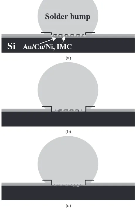
After 500 h aging of the Sn–1.8Bi–0.8Cu–0.6In bumps, 44.0% of Cu, and 9.8% of Ni were detected at the location ‘‘A’’ of the fracture surface shown in Fig. 6(d), indicating that the fracture took place between the solder and the IMC. At the location of ‘‘B’’ in Fig. 6(d), 25.8% of Al was detected, indicating that the fracture occurred between the Al-UBM and the IMC. Thus, it is concluded that the fracture at the interface periphery occurred mostly between the IMC and the Al, and in the center mostly between solder and IMC as shown schematically in Fig. 7(b).
The fracture mode after 1,000 h aging of the Sn–1.8Bi– 0.8Cu–0.6In bumps as shown in Figs. 6(e) and (f) was similar to that at 500 h aged bumps. From Figs. 6(a)–(f) it is found that the amount of exposed Al increased with aging time. This is because the Cu and Ni of the UBM diffuse into the
solder as the aging time increases, and react with Sn.18,19) Since the Cu and Ni layers used in this study are as thin as 0.4mm they were exhausted during aging by forming the IMC. It is thought that the characteristic of the IMC not to react with the Al-layer is the cause of the fracture between the Al-layer and the IMC. Thus, it is believed that the change of the fracture surface material from Ni and Cu to Al is the main factor to decrease the bond strength. Similarly, the complete exhaustion of a thin UBM with 0.3mmof Cu and 0.4mmof Ni, was observed earlier,20) and resulted in bond strength decrease. In plasma soldering21) the bond strength was improved by increasing UBM thickness, and hence in this study also thicker UBM is expected to reduce the strength decrease.
The schematics in Figs. 7(a)–(c) illustrate how the fracture mode changes with aging time. The Al layer (UBM) exposure starts at the pad edges and propagates into the center as the aging proceeds. In other words, the UBM
(a)
(b)
A
B
(c)
(d)
(e)
(f)
[image:4.595.112.486.70.522.2]completely is being consumed as aging time proceeds. The consumption starts first at the edge of the pads. A possible explanation is that during reflow the outer solder reaches melting temperature earlier than the inner solder so that IMC formation and UBM consumption starts earlier at the interface periphery.
3.3 Interfacial microstructure of Sn–1.8Bi–0.8Cu–0.6In solder on the Au/Cu/Ni/Al UBM
To characterize how the IMC formed between Sn–1.8Bi– 0.8Cu–0.6 solder and Au/Cu/Ni/Al UBM, samples were produced with 0, 500, and 1000 h aging time. To observe the IMC, the samples were cross-sectioned, polished up to 0.04mmand etched for 80 s in a solution of 5% HCl and 95% C2H5OH. The SEM picture of the as-reflowed sample is
shown in Fig. 8(a). Some Cu–Sn IMCs were observed into the solder. Cu–Ni–Sn IMCs along the interface were observed. EDS results are given in Table 1 and showed that the IMCs were composed of 48.6%Sn, 44.3%Cu, 6.7%Ni and 0.4%In. This composition is close to (Cu,Ni)6Sn5 based on
the Cu6Sn5 structure. With increasing aging time, dendritic
(Cu,Ni)6Sn5 changes into a round shape and its amount
decreases as seen in Figs. 8(a), (b), and (c) for samples aged 0, 500, and 1000 h, respectively.
The microstructure changes of the solder joints between Sn–1.8Bi–0.8Cu–0.6In solder and the UBM with increasing aging time are discussed in the following using Figs. 8(a)–
Solder bump
Si
Au/Cu/Ni, IMC
(a)
(b)
(c)
Fig. 7 Schematic diagrams showing fracture mechanism for aging times (a) as-reflowed, (b) 500 h, (c) 1000 h.
Cu6Sn5
(a)
(b)
(c)
[image:5.595.315.539.67.607.2]Fig. 8 SEM images of cross-sections showing the microstructure changes of the solder joints between the Sn–1.8Bi–0.7Cu–0.6In solder and the Si-wafer with aging time, (a) one cycle as-reflowed, (b) 500 h, and (c) 1000 h.
Table 1 EDS results showing IMC composition in mass% for as-reflowed and 1000 h aging time.
Sn Cu Ni In IMC
As-reflowed 48.6 44.3 6.7 0.4 (Cu,Ni)6Sn5
[image:5.595.52.284.94.453.2] [image:5.595.304.549.689.730.2]other words, the IMCs were flattened as aging time increased. Berry and Ames22)have reported that the IMCs spalled into the solder when Cu was consumed. Liu et al.23) reported similar results and suggested that the IMC changed to circle-type in shape when spalling began. The spalling in this study started before 500 h aging. Due to spalling the IMC thickness decreased about 58% from 2.9mmat 500 h aging to 1.2mm
after 1,000 h aging. Spalling of Cu6Sn5 occurs for thin-film
Cu-UBM but does not occur in bulk Cu.24) Liu et al.25)
reported that the shape change of the Cu–Sn compounds into spheres implies a high-energy interface. This shape change can results in nonwetting contact angle26)to the Al surface. Therefore their interfacial bonding is weak. Thus, the spalling could cause a decrease in the strength of solder joints.
Dendritic Cu6Sn5 was reported to be formed during
solidification due to the reaction of dissolved Cu with Sn.27) It is also known that in the Sn–3.5Ag/Cu bonding joint, Cu6Sn5 can form in the bulk solder by high Cu dissolution
into the molten solder and by Cu6Sn5broken from the bonded
interface.28)As seen in Fig. 8(a), Cu
6Sn5and (Cu,Ni)6Sn5in
the solder and at the interface between solder and UBM. Cu6Sn5 in the solder appears to be formed by the reaction
between Cu and Sn in the solder during melting and solidification. On the other hand, The dendritic (Cu,Ni)6Sn5
at the interface seems to be produced by dissolved Cu and Ni from the UBM during the reflow process. During aging, the (Cu,Ni)6Sn5 particles in the solder bulk as shown in
Figs. 8(b) and (c) broke away IMC in the bonded interface as it contains.
Cu3Sn IMC was not detected in either as-reflowed or the
1000 h aged condition. The reason why the Cu3Sn IMC was
not detected could be explained as follows. Generally, it is known that the activation energy to form Cu6Sn5between Cu
pads and Sn based solder is smaller than that of Cu3Sn.29)
Cu3Sn IMC grows with the consumption of Cu6Sn5 by the
diffusion of Cu from the UBM.30)Sharifet al.31)reported that the dissolution of Cu during reflow at 483 K was about 0.4 um in 500mmSn–Pb BGA balls. Kimet al.24)also concluded that the thickness of Cu consumed in Sn–Pb after 1 min reflow was about 0.36, 0.47 and 0.69mmat 473, 493, and 513 K respectively. Furthermore, the reaction rate of Cu with Pb-free solder is much faster than with Sn–Pb solder because of the high content of Sn in the solder and a channel effect in the Pb-free solders. Cu thickness deposited on the UBM in this study was very thin at 0.4mm. The reflow time above the melting temperature of 487 K in this reflow process was about 45.6 s and the peak temperature was set to 523 K. Therefore, it is thought that the 0.4mm Cu layer was completely consumed in the first reflow process and Ni participated in the reaction. So there is no Cu remaining to take part in the reaction with Cu6Sn5 to form Cu3Sn in the
UBM. To confirm the participation of Ni, EDS analysis was employed and the result as seen in Table 1 showed that 6.7% of Ni was present in the IMCs. From this analysis, it was confirmed that Cu was completely consumed in the first reflow process and was not available to form Cu3Sn on the
interface between the solder and UBM.
The bump formation of a solder paste using the new solder alloy, 1.8Bi–0.8Cu–0.6In, the morphology of the IMCs, and the shear strength of the bumps were studied. Sn–37Pb, Sn– 3.5Ag and Sn–36Pb–2Ag were used as reference materials for comparison. To make a bump on the UBM, the stencil printed pastes were reflow soldered in air at 523 K for Sn– 1.7Bi–0.8Cu–0.6In and Sn–3.5Ag and at 503 K for Sn–37Pb and Sn–36Pb–2Ag. The stencil-printed 1.8Bi–0.8Cu–0.6In paste formed bumps on the UBM after soldering and their average height was 260mm. However, craters were observed at the top or side of the bump, which can originate from gas escape from the molten solder. After a second reflow, the craters disappeared and the bumps were uniformly reshaped. The bond shear strengths of the bumps was highest for the Sn–1.8Bi–0.8Cu–0.6In bumps, 6.5N, followed by the strengths of the Sn–3.5Ag, Sn–37Pb and Sn–36Pb–2Ag bumps. The strength after aging 1000 h at 423 K decreased about 26, 26, and 37% for the Sn–1.8Bi–0.8Cu–0.6In, Sn– 3.5Ag, and Sn–36Pb–2Ag bumps, respectively. The aged strength of the new alloy showed the highest value. The fracture mode changed from solder- to UBM-fracture. The interfacial IMCs formed by the Sn–1.8Bi–0.8Cu–0.6In represented dendritic (Cu,Ni)6Sn5 in as-reflowed state, and
changed into the round shape with aging. Spalling of the interfacial IMCs into the solder started before 500 h aging, and the number of spalled particles was highest after 1000 h of aging. Consequently, the new solder alloy, Sn–1.7Bi– 0.8Cu–0.6In, revealed its feasibility for the application for solder bumping in terms of bond strength, interface structure, and reliability.
Acknowledgement
This work was supported by Korea Science and Engineer-ing Foundation (R01-2004-000-10572-0).
REFERENCES
1) D. J. Xie: Microelectron. Reliab.40(2000) 1191–1198.
2) J. H. Lau:Flip Chip Technology.(McGraw-Hill, 1996) xvii–xviii. 3) H. Ezawa, M. Miyata, S. Honma, H. Inoue, T. Tokuoka, J. Yoshioka
and M. Tsujimura: IEEE Trans. Electron. Packag. Manufact.34(2001) 275–281.
4) D. Manessis, R. Patzelt, A. Ostmann, R. Aschenbrenner and H. Reichl: Microelecton. Reliab.44(2004) 797–803.
5) E. Jung, K. Heinricht, J. Kloeser, R. Aschenbrenner and H. Reichl: Proc. ‘‘22nd IEEE/CPMT Berlin Int’l Electron., Manufact. Technol.
Symp.’’ (IEEE, 1998) pp. 90–98.
6) C. Kanchanomai, Y. Miyashita, Y. Mutoh and S. L. Mannan: Mater. Sci. Eng. A345(2003) 90–98.
7) Q. Lin, Z. Jie, W. Lai and H. Shuanggi: Proc. ‘‘ICEPT 5thint’l Conf.
Electron., Packag., Technol.’’ (2003) pp. 265–269.
8) I. Shohji, T. Yoshida, T. Takahashi and S. Hioki: Mater. Sci. Eng. A 366(2004) 50–55.
9) C.-W. Hwang and K. Suganuma: Mater. Sci. Eng. A373(2004) 187– 194.
10) M. Amagai, M. Watanabe, M. Omiya, K. Kishimoto and T. Shibuya: Microelectron. Reliab.42(2002) 951–966.
11) M.-I. Kim, B.-Y. Ahn and J.-P. Jung: J. Microelectr. Packg. Soc.8 (2001) 5–11.
61.
14) L. Huang, C. M. L. Wu, J. K. L. Lai and Y. C. Chan: J. Electron. Mater. 29(2000) 1021–1026.
15) S. W. Yoon, J. R. Soh, H. M. Lee and B. J. Lee: Acta Mater.45(1997) 951–960.
16) H. W. Miao and J. G. Duh: Mater. Chem. Phys.71(2001) 255–271. 17) M. Yunus, K. Srihari, J. M. Pitarresi and A. Primavera: Microelectron.
Reliab.43(2003) 2077–2086.
18) X. Ma, F. Wang, Y. Qian and F. Yoshida: Mater. Lett.57(2003) 3361– 3365.
19) M. He, Z. Chen and G. Qi: Acta Materialia.52(2004) 2047–2056. 20) J. K. Moon, J. P. Jung and Y. Zhou: Soldering Surf. Mount. Technol.17
(2005) 3–9.
21) J. W. Moon, K. I. Kang, J. Lee, J. P. Jung and Y. Zhou: J. Kor. Inst. Surf. Eng.36(2003) 373–378 (in Korean).
22) B. S. Berry and I. Ames: IBM, J. Res. Dev.13(1969) 286–296.
2780.
24) H. K. Kim and K. N. Tu: Appl. Phys. Lett.67(1995) 2002–2004. 25) C. Y. Liu, Chih Chen, A. K. Mal and K. N. Tu: J. Appl. Phys.85(1999)
3382–3386.
26) H. K. Kim, K. N. Tu and P. A. Totta: Appl. Phys. Lett.68(1996) 2204– 2206.
27) W. Yang, L. E. Felton and R. W. Messler, Jr.: J. Electron. Mater.24 (1995) 1465–1472.
28) W. Yang, R. W. Messler, Jr. and L. E. Felton: J. Electron. Mater.23 (1994) 765–772.
29) W. K. Choi and H. M. Lee: Scr. Mater.46(2002) 777–781. 30) Y. C. Chan, Alex C. K. So and J. K. L. Lai: Mater. Sci. Eng. B55
(1998) 5–13.