warwick.ac.uk/lib-publications
Original citation:
Morrison, C., Casteleiro, Catarina, Leadley, D. R. (David R.) and Myronov, Maksym. (2016) Complex quantum transport in a modulation doped strained Ge quantum well
heterostructure with a high mobility 2D hole gas. Applied Physics Letters, 109 (10). 102103.
Permanent WRAP URL:
http://wrap.warwick.ac.uk/81465
Copyright and reuse:
The Warwick Research Archive Portal (WRAP) makes this work by researchers of the University of Warwick available open access under the following conditions. Copyright © and all moral rights to the version of the paper presented here belong to the individual author(s) and/or other copyright owners. To the extent reasonable and practicable the material made available in WRAP has been checked for eligibility before being made available.
Copies of full items can be used for personal research or study, educational, or not-for-profit purposes without prior permission or charge. Provided that the authors, title and full bibliographic details are credited, a hyperlink and/or URL is given for the original metadata page and the content is not changed in any way.
Publisher’s statement:
This article may be downloaded for personal use only. Any other use requires prior permission of the author and AIP Publishing.
The following article appeared in Morrison, C., Casteleiro, Catarina, Leadley, D. R. (David R.) and Myronov, Maksym. (2016) Complex quantum transport in a modulation doped strained Ge quantum well heterostructure with a high mobility 2D hole gas. Applied Physics Letters, 109 (10). 102103. and may be found at http://dx.doi.org/10.1063/1.4962432
A note on versions:
The version presented in WRAP is the published version or, version of record, and may be cited as it appears here.
Complex quantum transport in a modulation doped strained Ge quantum
well heterostructure with a high mobility 2D hole gas
C.Morrison,a)C.Casteleiro,D. R.Leadley,and M.Myronov
Department of Physics, University of Warwick, Coventry CV4 7AL, United Kingdom
(Received 27 May 2016; accepted 26 August 2016; published online 7 September 2016)
The complex quantum transport of a strained Ge quantum well (QW) modulation doped heterostructure with two types of mobile carriers has been observed. The two dimensional hole gas (2DHG) in the Ge QW exhibits an exceptionally high mobility of 780 000 cm2/Vs at temperatures below 10 K. Through analysis of Shubnikov de-Haas oscillations in the magnetoresistance of this 2DHG below 2 K, the hole effective mass is found to be 0.065 m0. Anomalous conductance peaks
are observed at higher fields which deviate from standard Shubnikov de-Haas and quantum Hall effect behaviour due to conduction via multiple carrier types. Despite this complex behaviour, anal-ysis using a transport model with two conductive channels explains this behaviour and allows key physical parameters such as the carrier effective mass, transport, and quantum lifetimes and con-ductivity of the electrically active layers to be extracted. This finding is important for electronic device applications, since inclusion of highly doped interlayers which are electrically active, for enhancement of, for example, room temperature carrier mobility, does not prevent analysis of quantum transport in a QW.Published by AIP Publishing.[http://dx.doi.org/10.1063/1.4962432]
Epitaxially grown Ge is of great interest for device appli-cations, primarily due to its high hole mobility1,2and compati-bility with epitaxial Si technology. Recently, epitaxially grown layers of Ge grown on SiGe on a standard Si(001) sub-strate have been shown to have extremely high room tempera-ture hole mobility of up to 4500 cm2/Vs due to formation of a two dimensional hole gas (2DHG).2,3 Compressive strain of the Ge epilayer induced by epitaxial growth results in 2DHG formation and the holes have enhanced mobility due to their lower effective mass and reduced scattering factors. Low tem-perature 2DHG mobility in excess of 1.3106cm2/Vs has been achieved.1,4–6The study of quantum transport behaviour in these 2DHGs at low temperatures, in particular, the Shubnikov de-Haas (SdH) oscillations that arise from Landau levels created under an applied magnetic field, allows us to determine the key parameters such as effective mass, as well as the carrier densities and diffusive and quantum transport scattering parameters.
Previously, low temperature magnetotransport has been studied for Ge quantum wells (QWs) but primarily on struc-tures with comparatively low 2DHG mobility and much higher carrier densities.7–10For example, Miuraet al.studied quantum transport in a compressively strained Ge QW with a 2DHG mobility of 23 800 cm2/Vs and a carrier density of 2.41012cm2.11Prior to the recent report of hole mobility in excess of 1106cm2/Vs at a carrier density of 2.91011cm2 in a Ge QW,1the record value of mobility was 120 000 cm2/Vs with a carrier density of 8.51011cm2.12The study of quan-tum transport in high mobility Ge 2DHGs since this discovery has primarily focussed on the spin-orbit interaction in hetero-structures of this type13–15and on the composite fermions and the fractional quantum Hall effect in high magnetic fields.4–6 Here, we study low temperature quantum transport in a Ge QW
heterostructure, modulation doped with 21018cm3of boron (B) and a delta layer of B. This doped heterostructure has a low temperature hole mobility of 780 000 cm2/Vs, approaching the record value.
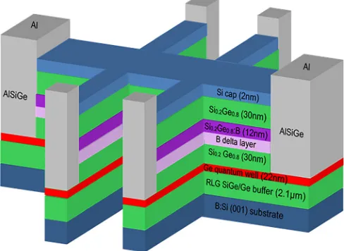
The heterostructure studied here was grown by reduced pressure chemical vapor deposition onto a 100 mm n-type Si (001) substrate. The structure is shown schematically in Figure 1, and the corresponding band structure simulated using a Poisson-Schr€odinger method may be found in the study by Forondaet al., Figure 3.14A reverse linearly graded (RLG) buffer layer was first grown onto the substrate, fol-lowed by the active region. A doping concentration of 21018cm3B was created in the supply layer and a delta layer of B directly below this layer. The delta layer was inserted to maximise the room temperature 2DHG mobility to 4500 cm2V1s1in this Ge QW.2However, because the
FIG. 1. (a) Schematic of the Ge quantum well heterostructure studied here, showing the Hall bar geometry used for the magnetotransport measurements. The primary active transport layer (location of the 2DHG) is indicated in red.
a)Author to whom correspondence should be addressed. Electronic mail:
[image:2.612.316.560.530.708.2]boron doping level in the delta layer is above the metal-insulator transition it will be conductive even at very low temperatures and cause deviations from the norm in quantum phenomena like Shubnikov de-Haas oscillations in the mag-netoresistance and the quantum Hall resistance plateaus at low temperatures. The density of Boron in the delta doped region was determined to be 51018cm3using Secondary Ion Mass Spectrometry (SIMS). The thicknesses of the layers were confirmed by cross-sectional transmission elec-tron microscopy. A detailed study of the material properties of this heterostructure has been published elsewhere.3
Magnetotransport, Hall effect, and resistivity measure-ments were performed using a Hall bar geometry produced using photo-lithography. Thermally evaporated Al was used as a contact material, post-annealed to form a contact with the QW. The Ge QW mesa was defined by reactive ion etch-ing in an SF6:O2mixture down to the Si substrate. All
con-tacts were found to exhibit Ohmic behaviour at 20 K and below, with typical contact resistances between 400X and 1000X at 20 K. All magnetotransport measurements were performed using an ac current excitation of 100 nA at a fre-quency of 19.77 Hz. The magnetic field was applied perpen-dicular to the plane of the device. Sheet resistance and Hall coefficient were measured from room temperature down to 0.3 K, from which the sheet carrier density and Hall mobility were calculated. Carrier freeze-out does not occur at low temperatures, and the Ge QW demonstrates good, metallic transport behaviour indicative of the presence of 2D confine-ment. Mobility at the lowest temperatures is very high (780 000 cm2/Vs), approaching the record value in this class of heterostructures.1The carrier density is 21011cm2 at 0.3 K, indicating a relatively high transferal of carriers from the doping layer into the QW region.
Magnetotransport and Hall effect measurements were made under an applied magnetic fieldBof up to 12 T perpen-dicular to the Hall bar, for temperaturesTfrom 300 mK up to 10 K. The results at 338 mK are shown in Figure 2; the data shown in the figure represent the average of the magne-toresistance and Hall resistance magnitudes across both mag-netic field polarities. Clear SdH oscillations are observed; however, the oscillatory behavior is unusually complex due to the presence of two parallel conducting layers: at the low-est temperatures, there are SdH minima corresponding to the even integer filling factor at lowB; above 0.3 T, odd integer SdH minima also appear due to Zeeman splitting; however, above about 0.6 T, sharp peaks at all integer filling factors start to dominate the resistivity. As the temperature is increased, the transition from minima to maxima at the inte-ger filling factor moves to higherBand the amplitude of the peaks decreases. These peaks cannot be explained by con-ventional Shubnikov de-Haas theory of a single carrier type. The Hall resistance is also complex, with no observable quantum Hall plateaus and instead sharp minima occurring in the Hall resistance at the integer filling factor, with tem-perature dependent amplitude. By plotting the magnetocon-ductance of the structure instead it is possible to isolate the conductance due to parallel conduction in the heterostruc-ture. This quantity is plotted in Figure3for the lowest tem-perature studied (338 mK), again averaged across both polarities of magnetic field. The dashed orange line indicates
[image:3.612.338.535.55.349.2]the base conductance (30lS) of the layers conducting in par-allel to the 2DHG, which may be compared to the much larger conductance of 24 900lS in the QW. This corre-sponds to only 0.1% electrical conductance via the B delta layer. Most of the layers in the heterostructure are intention-ally undoped and therefore are unlikely to form a parallel conduction channel at low temperatures due to carrier freeze-out. We therefore suggest that the main source of con-duction parallel to the 2DHG is in the B modulation doping
FIG. 3. Magnetoconductance at 338 mK, averaged across both magnetic field polarities. The dashed blue line shows background conductance as a result of parallel conduction in the region of the doping layer. The conduc-tance of the parallel conduction layer is 30lS and therefore the conductance in the 2DHG only may be calculated as 24 900lS. The parallel conductance is only 0.1% of the total conductance of the heterostructure.
FIG. 2. (a) Magnetoresistance and (b) Hall effect measurement at 338 mK for the B modulation doped 2DHG for an applied magnetic field up to 12 T, showing the magnitude of the magnetoresistance and Hall resistance aver-aged across both magnetic field polarities. Insets: resistance data at low fields. Red arrows indicate the position of anomalous resistance peaks. Red dashed lines indicate the expected position of integer quantum Hall plateaus. 102103-2 Morrisonet al. Appl. Phys. Lett.109, 102103 (2016)
[image:3.612.340.535.556.705.2]delta layer. Due to the high carrier occupation remaining in this region, we may conclude that we have achieved the limit of 2DHG carrier density in the QW achievable by modula-tion doping for a given amount of biaxial compressive strain and consequently the valence band offset of the Ge QW. Increasing the strain present in the QW region by, for exam-ple, reducing the percentage of Ge in the buffer layer is expected to increase the carrier density limit in the 2DHG. This has the additional advantage of increasing the energy gap between the heavy and light hole bands and conse-quently reducing interband scattering, which would result in a further increase of hole mobility in the 2DHG.
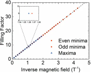
By plotting the inverse field position of the minima/ maxima in the magnetoresistance as a function of quantum Hall filling factor, it is possible to extract the sheet carrier density of the 2DHG producing the oscillations. This plot is shown in Figure4for the lowest temperature (338 mK). The gradient of this curve is equal tohpe, wherepis the sheet hole density of the 2DHG. Performing a linear fit to the data in Figure4gives a sheet hole density of 2.01011cm2. This value agrees with the sheet carrier density calculated using the low field Hall resistance as previously shown. This analy-sis shows that, despite the apparently complex oscillatory behaviour observed, all the oscillations arise due to the exis-tence of Landau levels created from a single, fundamental energy level in the QW.
The peaks in magnetoresistance as a function of mag-netic field in the low field regime may be used to calculate the effective mass of carriers in the conduction region(s) by an iterative process. The analytical equation that describes Shubnikov-de Haas oscillations is as follows:16,17
Dqxxð ÞB
qxxð Þ0
¼4 cos 2pEFm
heB
exp pm
a
eBst
w
sinhð Þw ; (1)
whereEFis the Fermi energy,ais the Dingle ratio (sqst, where stis the transport scattering time andsqis the quantum
scat-tering time), andw¼2p2kBTm
heB .
Plots of two simultaneous equations derived from this equation that may be used to iteratively solve for the effec-tive mass and Dingle ratio are shown in Figure5.18 These plots represent the final iteration of the solution using an
iterative step of 0.005 m0. Two clear strata of points are
observed, corresponding to carriers with differing quantum lifetimes. We find that a solution is obtained, for both strata analysed individually, for an effective mass m*¼0.065 m0.
However, the Dingle ratio varies considerably. For the main stratum, illustrated by a black dashed line, the Dingle ratio is found to be 18, increasing to 33 for the second stratum (red dashed line).
The transport scattering time for holes in the 2DHG may be calculated using the expressionst¼m
l
H
e , wherelHis the
Hall mobility. Inserting the Hall mobility at 338 mK (780 000 cm2/Vs) and the effective mass yields a value of
st¼29 ps, corresponding to a transport scattering length of
5.7lm. Using this value for st and the calculated Dingle
ratios gives quantum scattering timessq¼1.6 ps, and 0.87 ps
for the two carrier lifetimes revealed through the effective mass analysis.
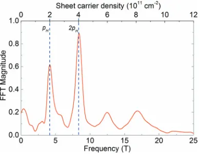
[image:4.612.339.536.50.385.2]The carrier density of the occupied energy levels in the QW may be calculated from the Shubnikov-de Haas oscilla-tions, by a fast Fourier transform method. First, the oscillatory magnetoresistance behaviour is isolated by subtraction of a quadratic resistance background due to ordinary (geometric) magnetoresistance. These data are then plotted as a function of inverse magnetic field and a fast Fourier transform is per-formed. The resulting spectrum exhibits peaks at given fre-quencies (units of T) which correspond to carrier densities in the QW via the relation p¼pf eh, wheref is the frequency of FIG. 4. Plot of inverse field positions of minima/maxima in the
magnetoresis-tance against filling factor, at a temperature of 338 mK. The carrier density extracted from a linear fit to the data is 2.01011cm2. The inset resolves
the separation of maxima and minima in inverse magnetic field space.
[image:4.612.78.272.570.725.2]oscillation. The spectrum resulting from transformation of the 338 mK magnetoresistance data, below the first anomalous conductance peak, is shown in Figure 6. Clear peaks are observed at the Hall carrier density (21011cm2) and at twice the Hall carrier density (41011cm2). The second peak may either be a harmonic or be indicative of quantum transport in another layer, for example, the highly B doped SiGe region. However, as shown in Figure4, all Shubnikov de-Haas maxima/minima can be attributed to Landau levels generated from the Fermi energy for carriers at the Hall carrier density (21011cm2). We can therefore attribute the second peak to harmonic generation due to the onset of Zeeman split peaks. The two additional, lower amplitude peaks at higher carrier densities are further harmonics corresponding to three and four times the first sub-band density, respectively.
Assuming a carrier density of 11012cm2 for the delta doped B layer, based on the SIMS-determined dopant density and a typical activation approximately 50%, the background conductivity extracted from Figure 3 gives an approximate value for the mobility of 200 cm2/Vs at 338 mK. The mobility in this region is primarily limited by the high degree of ionised impurity scattering from acceptor ions, and this value agrees well with the expected value for mobility for Ge at this doping level. For most applications, one does not wish to have a parallel layer as this will compli-cate device designs and hinder performance. For applica-tions, it is desirable to instead achieve higher carrier density (and mobility) through the use of an electrostatic gate, avoid-ing the use of dopant layers altogether. In such a structure, a doping layer would in fact hinder gate performance due to screening of the gate potential and is so further undesirable. The findings in this study help in the design of device param-eters without requiring a complex gate optimisation process.
In summary, a high mobility (780 000 cm2/Vs) 2DHG has been created in a strained Ge QW structure, through B modulation doping. The mobility and carrier density were measured through Hall effect measurements at temperatures
between 0.3 K and 300 K, revealing a low temperature car-rier density of 21011cm2. Low temperature magnetore-sistance measurements show a complex Shubnikov de-Haas oscillatory behavior. Analysis of the oscillation amplitudes yields an effective mass m*¼0.065 m0. Fast Fourier
trans-form analysis shows peaks at two frequencies, corresponding to carriers at carrier densities of 21011cm2 and 41011cm2, respectively. The first peak agrees with the carrier density extracted via Hall effect analysis, and the sec-ond peak is a harmonic of the fundamental peak due to Zeeman splitting. The lack of quantum transport in the paral-lel conduction layer is consistent with the B doping region being too narrow for 2D confinement to occur. A two chan-nel model allows us to extract key electrical parameters including the conductivity of the channels and their respec-tive mobilities. The Hall mobility of the heterostructure cor-responds closely to that of the QW alone, due to the large difference in mobilities and conduction being primarily through the QW region. The parallel, low mobility transport channel is consistent with electronic transport by carriers in the highly B doped region of the heterostructure.
This work was supported by the EPSRC funded “Spintronic device physics in Si/Ge Heterostructures” EP/J003263/1 and “Platform Grant” No. EP/J001074/1 Projects.
1A. Dobbie, M. Myronov, R. J. H. Morris, A. H. A. Hassan, M. J. Prest, V.
A. Shah, E. H. C. Parker, T. E. Whall, and D. R. Leadley, Appl. Phys. Lett.101, 172108 (2012).
2
M. Myronov, C. Morrison, J. Halpin, S. Rhead, J. Foronda, and D. Leadley,Solid-State Electron.110, 35 (2015).
3
M. Myronov, C. Morrison, J. Halpin, S. Rhead, C. Casteleiro, J. Foronda, V. A. Shah, and D. Leadley,Jpn. J. Appl. Phys.53, 04EH02 (2014).
4
Q. Shi, M. A. Zudov, C. Morrison, and M. Myronov,Phys. Rev. B91, 201301 (2015).
5
Q. Shi, M. A. Zudov, C. Morrison, and M. Myronov,Phys. Rev. B91, 241303 (2015).
6
Q. Shi, M. A. Zudov, C. Morrison, and M. Myronov,Phys. Rev. B92, 161405 (2015).
7T. Irisawa, M. Myronov, O. A. Mironov, E. H. C. Parker, K. Nakagawa,
M. Murata, S. Koh, and Y. Shiraki,Appl. Phys. Lett.82, 1425 (2003).
8B. R€oßner, G. Isella, and H. V. K€anel,Appl. Phys. Lett.
82, 754 (2003).
9
K. Sawano, Y. Kunishi, Y. Shiraki, K. Toyama, T. Okamoto, N. Usami, and K. Nakagawa,Appl. Phys. Lett.89, 162103 (2006).
10
Y. F. Komnik,Low Temp. Phys.32, 82 (2006).
11
N. Miura, N. V. Kozlova, K. D€orr, J. Freudenberger, L. Schultz, O. Drachenko, K. Sawano, and Y. Shiraki, J. Low Temp. Phys.159, 222 (2010).
12
B. R€ossner, D. Chrastina, G. Isella, and H. von K€anel,Appl. Phys. Lett.
84, 3058 (2004).
13C. Morrison, P. Wisniewski, S. D. Rhead, J. Foronda, D. R. Leadley, and
M. Myronov,Appl. Phys. Lett.105, 182401 (2014).
14J. Foronda, C. Morrison, J. E. Halpin, S. D. Rhead, and M. Myronov,
J. Phys.: Condens. Matter27, 022201 (2014).
15C. Morrison, J. Foronda, P. Wisniewski, S. D. Rhead, D. R. Leadley, and
M. Myronov,Thin Solid Films602, 84 (2016).
16A. Isihara and L. Smrcka,J. Phys. C: Solid State Phys.19, 6777 (1986). 17P. Coleridge, R. Stoner, and R. Fletcher,Phys. Rev. B
39, 1120 (1989).
18
[image:5.612.78.273.54.204.2]Y. F. Komnik, V. V. Andrievskii, I. B. Berkutov, S. S. Kryachko, M. Myronov, and T. E. Whall,Low Temp. Phys.26, 609 (2000).
FIG. 6. Fast Fourier transform of the low field (<0.8 T) magnetoresistance at 338 mK as a function of inverse field. The upper x-axis shows the fre-quency of oscillation transformed into sheet carrier density.
102103-4 Morrisonet al. Appl. Phys. Lett.109, 102103 (2016)