Motorola reserves the right to make changes without further notice to any products herein. Motorola makes no warranty, representation or guarantee regarding the suitability of its products for any particular purpose, nor does Motorola assume any liability arising out of the application or use of any product or circuit, and specifically disclaims any and all liability, including without limitation consequential or incidental damages. “Typical” parameters which may be provided in Motorola data sheets and/or specifications can and do vary in different applications and actual performance may vary over time. All operating parameters, including “Typicals” must be validated for each customer application by customer’s technical experts. Motorola does not convey any license under its patent rights nor the rights of others. Motorola products are not designed, intended, or authorized for use as components in systems intended for surgical implant into the body, or other applications intended to support or sustain life, or for any other application in which the failure of the Motorola product could create a situation where personal injury or death may occur. Should Buyer purchase or use Motorola products for any such unintended or unauthorized application, Buyer shall indemnify and hold Motorola and its officers, employees, subsidiaries, affiliates, and distributors harmless against all claims, costs, damages, and expenses, and reasonable attorney fees arising out of, directly or indirectly, any claim of personal injury or death associated with such unintended or unauthorized use, even if such claim alleges that Motorola was negligent regarding the design or manufacture of the part. Motorola and are registered trademarks of Motorola, Inc. Motorola, Inc. is an Equal Opportunity/Affirmative Action Employer.
©Motorola, Inc., 2001
HCS12 Serial Communications Interface
(SCI)
Block Guide
V02.08
Original Release Date: 29 Oct 2001 Revised: 16 Apr 2004
Revision History
Version Number
Revision Date
Effective
Date Author Description of Changes
00.10 06/04/1999 Original draft. Distributed only within Motorola 00.10 06/04/1999 Original draft. Distributed only within Motorola
00.20 09/01/1999 Specifications modified for Barracuda SCI. Changes based on change request.
00.30 09/20/1999 Specification updated after review at Munich
00.40 10/22/1999 Specification updated after changes in the number of inter-rupt signals from SCI
00.50 01/25/2000 Specification document updated after internal Design data-base review.
00.60 02/01/2000 TXDIR bit shifted from register SCIDRH (bit 0) to register SCISR2 (bit 1).
02.00 10/19/2000 BRK13 bit included in the SCISR2 (bit 3)
02.01 04/02/2001 Updated according to feedback concerning SRS v2 andadditional rules compliance
02.02 07/19/2001 Document names have been added
Names and Variable definitions have been hidden 02.03 10/10/2001 Correct the RWU definition in the SCI CR2 register andreplace the STAR12 by HCS12.
02.04 03/07/2002 New document numbering. Corrected typos.
Removed document order number except from Cover Sheet 02.05 06/24/2002 Correct the statement about the source of baud rategeneration error in section 4.3.
02.06 11/15/2002 Update Table 4-3 to use more general module clock frequency 25 MHz instead of 10.2 MHz
02.07 07/05/2003 Updated according to SRS3.0
Table of Contents
Section 1 Introduction
1.1 Overview. . . .11
1.2 Features . . . .11
1.3 Modes of Operation . . . .12
Section 2 External Signal Description
2.1 Overview. . . .132.2 Detailed Signal Descriptions. . . .13
2.2.1 TXD- SCI Transmit Pin. . . .13
2.2.2 RXD-SCI Receive Pin . . . .13
Section 3 Memory Map/Register Definition
3.1 Overview. . . .133.2 Module Memory Map . . . .13
3.3 Register Descriptions . . . .14
3.3.1 SCI Baud Rate Registers . . . .14
3.3.2 SCI Control Register 1 . . . .15
3.3.3 SCI Control Register 2 . . . .17
3.3.4 SCI Status Register 1. . . .18
3.3.5 SCI Status Register 2. . . .21
3.3.6 SCI Data Registers . . . .21
Section 4 Functional Description
4.1 General. . . .224.2 Data Format . . . .23
4.3 Baud Rate Generation . . . .24
4.4 Transmitter . . . .26
4.4.1 Transmitter Character Length . . . .26
4.4.2 Character Transmission . . . .26
4.4.3 Break Characters . . . .28
4.4.4 Idle Characters. . . .28
4.5 Receiver . . . .29
4.5.2 Character Reception . . . .30
4.5.3 Data Sampling . . . .30
4.5.4 Framing Errors . . . .34
4.5.5 Baud Rate Tolerance . . . .34
4.5.5.1 Slow Data Tolerance . . . 35
4.5.5.2 Fast Data Tolerance . . . 36
4.5.6 Receiver Wakeup. . . .36
4.5.6.1 Idle input line wakeup (WAKE = 0) . . . 37
4.5.6.2 Address mark wakeup (WAKE = 1) . . . 37
4.6 Single-Wire Operation . . . .37
4.7 Loop Operation. . . .38
Section 5 Initialization/Application Information
5.1 Reset Initialization . . . .395.2 Modes of Operation . . . .39
5.2.1 Run Mode. . . .39
5.2.2 Wait Mode . . . .39
5.2.3 Stop Mode . . . .39
5.3 Interrupt Operation . . . .39
5.3.1 System Level Interrupt Sources . . . .39
5.3.2 Interrupt Descriptions . . . .40
5.3.3 TDRE Description . . . .40
5.3.4 TC Description . . . .40
5.3.5 RDRF Description . . . .40
5.3.6 OR Description. . . .40
5.3.7 IDLE Description . . . .41
List of Figures
Figure 1-1 SCI Block Diagram . . . .11
Figure 3-1 SCI Register Quick Reference. . . .14
Figure 3-2 SCI Baud Rate Registers (SCI BDH/L) . . . .15
Figure 3-3 SCI Control Register 1 (SCICR1) . . . .15
Figure 3-4 SCI Control Register 2 (SCICR2) . . . .17
Figure 3-5 SCI Status Register 1 (SCISR1) . . . .18
Figure 3-6 SCI Status Register 2 (SCISR2) . . . .21
Figure 3-7 SCI Data Registers (SCIDRH/L) . . . .22
Figure 4-1 SCI Block Diagram . . . .23
Figure 4-2 SCI Data Formats . . . .24
Figure 4-3 Transmitter Block Diagram . . . .26
Figure 4-4 SCI Receiver Block Diagram . . . .29
Figure 4-5 Receiver Data Sampling . . . .30
Figure 4-6 Start Bit Search Example 1 . . . .32
Figure 4-7 Start Bit Search Example 2 . . . .32
Figure 4-8 Start Bit Search Example 3 . . . .33
Figure 4-9 Start Bit Search Example 4 . . . .33
Figure 4-10 Start Bit Search Example 5 . . . .34
Figure 4-11 Start Bit Search Example 6 . . . .34
Figure 4-12 Slow Data . . . .35
List of Tables
Table 3-1 Module Memory Map . . . .13
Table 3-2 Loop Functions . . . .16
Table 4-2 Example of 9-Bit Data Formats . . . .24
Table 4-1 Example of 8-bit Data Formats . . . .24
Table 4-3 Baud Rates (Example: Module Clock = 25MHz) . . . .25
Table 4-4 Start Bit Verification . . . .31
Table 4-5 Data Bit Recovery . . . .31
Table 4-6 Stop Bit Recovery . . . .31
Preface
The SCI allows full duplex, asynchronous, serial communication between the CPU and remote devices, including other CPUs. The SCI transmitter and receiver operate independently, although they use the same baud rate generator. The CPU monitors the status of the SCI, writes the data to be transmitted, and processes received data.
Terminology
IRQ: Interrupt Request
LSB: Least Significant Bit
MSB: Most Significant Bit
NRZ: Non-Return-to-Zero
RZI: Return-to-Zero-Inverted
RXD: Receive Pin
SCI : Serial Communication Interface
Section 1 Introduction
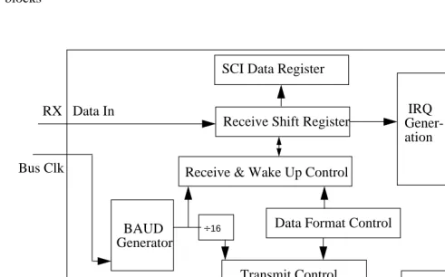
[image:11.792.65.556.176.482.2]This block guide provide an overview of Serial Communication Interface (SCI) module.
Figure 1-1 is a high level block diagram of the SCI module, showing the interaction of various function blocks
Figure 1-1 SCI Block Diagram
1.1 Overview
The SCI allows asynchronous serial communications with peripheral devices and other CPUs.
1.2 Features
The SCI includes these distinctive features:
• Full-duplex operation
• Standard mark/space non-return-to-zero (NRZ) format SCI Data Register
Receive Shift Register
Receive & Wake Up Control
Data Format Control
Transmit Control
Transmit Shift Register
SCI Data Register BAUD Generator IRQ IRQ IDLE RDRF/OR TDRE TC RX Data In
÷16 IRQ IRQ IRQ Bus Clk ation ration TXData Out IRQ O
IRQ To CPU
• 13-bit baud rate selection
• Programmable 8-bit or 9-bit data format
• Separately enabled transmitter and receiver
• Programmable transmitter output parity
• Two receiver wake up methods:
– Idle line walk-up
– Address mark walk-up
• Interrupt-driven operation with eight flags:
– Transmitter empty
– Transmission complete
– Receiver full
– Idle receiver input
– Receiver overrun
– Noise error
– Framing error
– Parity error
• Receiver framing error detection
• Hardware parity checking
• 1/16 bit-time noise detection
1.3 Modes of Operation
The SCI functions the same in normal, special, and emulation modes. It has two low power modes, wait ant stop modes.
• Run Mode
• Wait Mode
• Stop Mode
2.1 Overview
The SCI module has a total of 2 external pins:
2.2 Detailed Signal Descriptions
2.2.1 TXD- SCI Transmit Pin
This pin serves as transmit data output of SCI.
2.2.2 RXD-SCI Receive Pin
This pin serves as receive data input of the SCI.
Section 3 Memory Map/Register Definition
3.1 Overview
This section provides a detailed description of all memory and registers.
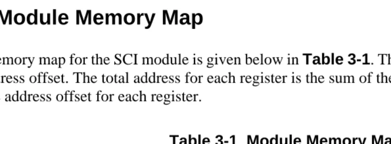
3.2 Module Memory Map
[image:13.792.115.500.475.617.2]The memory map for the SCI module is given below inTable 3-1. The Address listed for each register is the address offset. The total address for each register is the sum of the base address for the SCI module and the address offset for each register.
Table 3-1 Module Memory Map
Offset Use Access
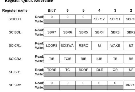
Register Quick Reference
Figure 3-1 SCI Register Quick Reference
3.3 Register Descriptions
This section consists of register descriptions in address order. Each description includes a standard register diagram with an associated figure number. Writes to a reserved register location do not have any effect and reads of these locations return a zero. Details of register bit and field function follow the register diagrams, in bit order.
3.3.1 SCI Baud Rate Registers
Register name Bit 7 6 5 4 3 2 1 Bit 0 Addr.
offset
SCIBDH Read: 0 0 0 SBR12 SBR11 SBR10 SBR9 SBR8 $_0
Write:
SCIBDL Read: SBR7 SBR6 SBR5 SBR4 SBR3 SBR2 SBR1 SBR0 $_1 Write:
SCICR1 Read: LOOPS SCISWAI RSRC M WAKE ILT PE PT $_2 Write:
SCICR2 Read: TIE TCIE RIE ILIE TE RE RWU SBK $_3
Write:
SCISR1 Read: TDRE TC RDRF IDLE OR NF FE PF $_4
Write:
SCISR2 Read: 0 0 0 0 0 BRK13 TXDIR RAF $_5
Write:
SCIDRH Read: R8 T8 0 0 0 0 0 0 $_6
Write:
SCIDRL Read: R7 R6 R5 R4 R3 R2 R1 R0 $_7
Write: T7 T6 T5 T4 T3 T2 T1 T0
= Reserved or unimplemented
Register address: $_0
7 6 5 4 3 2 1 0
R 0 0 0
SBR12 SBR11 SBR10 SBR9 SBR8 W
RESET: 0 0 0 0 0 0 0 0
Figure 3-2 SCI Baud Rate Registers (SCI BDH/L)
The SCI Baud Rate Register is used by the counter to determine the baud rate of the SCI. The formula for calculating the baud rate is:
SCI baud rate = SCI module clock / (16 x BR),
where BR is the content of the SCI baud rate registers, bits SBR12 through SBR0. The baud rate registers can contain a value from 1 to 8191.
Read: anytime. If only SCIBDH is written to, a read will not return the correct data until SCIBDL is written to as well, following a write to SCIBDH.
Write: anytime
SBR12 - SBR0 - SCI Baud Rate Bits
The baud rate for the SCI is determined by these 13 bits.
NOTE: The baud rate generator is disabled until the TE bit or the RE bit is set for the first time after reset. The baud rate generator is disabled when BR = 0.
NOTE: Writing to SCIBDH has no effect without writing to SCIBDL, since writing to SCIBDH puts the data in a temporary location until SCIBDL is written to.
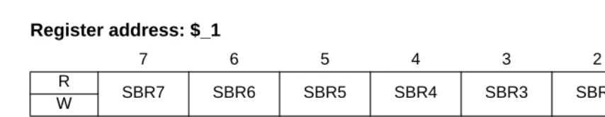
[image:15.792.95.522.69.151.2]3.3.2 SCI Control Register 1
Figure 3-3 SCI Control Register 1 (SCICR1)
Read: anytime
Register address: $_1
7 6 5 4 3 2 1 0
R
SBR7 SBR6 SBR5 SBR4 SBR3 SBR2 SBR1 SBR0
W
RESET: 0 0 0 0 0 1 0 0
= Unimplemented or Reserved
Register address: $_2
7 6 5 4 3 2 1 0
R
LOOPS SCISWAI RSRC M WAKE ILT PE PT
W
RESET: 0 0 0 0 0 0 0 0
Write: anytime
LOOPS - Loop Select Bit
LOOPS enables loop operation. In loop operation, the RXD pin is disconnected from the SCI and the transmitter output is internally connected to the receiver input. Both the transmitter and the receiver must be enabled to use the loop function.
1 = Loop operation enabled 0 = Normal operation enabled
The receiver input is determined by the RSRC bit.
SCISWAI — SCI Stop in Wait Mode Bit SCISWAI disables the SCI in wait mode.
1 = SCI disabled in wait mode 0 = SCI enabled in wait mode
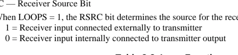
RSRC — Receiver Source Bit
When LOOPS = 1, the RSRC bit determines the source for the receiver shift register input. 1 = Receiver input connected externally to transmitter
0 = Receiver input internally connected to transmitter output
M — Data Format Mode Bit
MODE determines whether data characters are eight or nine bits long. 1 = One start bit, nine data bits, one stop bit
0 = One start bit, eight data bits, one stop bit
WAKE — Wakeup Condition Bit
WAKE determines which condition wakes up the SCI: a logic 1 (address mark) in the most significant bit position of a received data character or an idle condition on the RXD.
1 = Address mark wakeup 0 = Idle line wakeup
ILT — Idle Line Type Bit
ILT determines when the receiver starts counting logic 1s as idle character bits. The counting begins either after the start bit or after the stop bit. If the count begins after the start bit, then a string of logic 1s preceding the stop bit may cause false recognition of an idle character. Beginning the count after the stop bit avoids false idle character recognition, but requires properly synchronized transmissions.
[image:16.792.103.509.341.436.2]1 = Idle character bit count begins after stop bit 0 = Idle character bit count begins after start bit
Table 3-2 Loop Functions
LOOPS RSRC Function
0 x Normal operation
PE — Parity Enable Bit
PE enables the parity function. When enabled, the parity function inserts a parity bit in the most significant bit position.
1 = Parity function enabled 0 = Parity function disabled
PT — Parity Type Bit
PT determines whether the SCI generates and checks for even parity or odd parity. With even parity, an even number of 1s clears the parity bit and an odd number of 1s sets the parity bit. With odd parity, an odd number of 1s clears the parity bit and an even number of 1s sets the parity bit.
1 = Odd parity 0 = Even parity
[image:17.792.96.525.286.370.2]3.3.3 SCI Control Register 2
Figure 3-4 SCI Control Register 2 (SCICR2)
Read: anytime
Write: anytime
TIE — Transmitter Interrupt Enable Bit
TIE enables the transmit data register empty flag, TDRE, to generate interrupt requests. 1 = TDRE interrupt requests enabled
0 = TDRE interrupt requests disabled
TCIE — Transmission Complete Interrupt Enable Bit
TCIE enables the transmission complete flag, TC, to generate interrupt requests. 1 = TC interrupt requests enabled
0 = TC interrupt requests disabled
RIE — Receiver Full Interrupt Enable Bit
RIE enables the receive data register full flag, RDRF, or the overrun flag, OR, to generate interrupt requests.
1 = RDRF and OR interrupt requests enabled 0 = RDRF and OR interrupt requests disabled
ILIE — Idle Line Interrupt Enable Bit
Register address: $_3
7 6 5 4 3 2 1 0
R
TIE TCIE RIE ILIE TE RE RWU SBK
W
RESET: 0 0 0 0 0 0 0 0
ILIE enables the idle line flag, IDLE, to generate interrupt requests. 1 = IDLE interrupt requests enabled
0 = IDLE interrupt requests disabled
TE — Transmitter Enable Bit
TE enables the SCI transmitter and configures the TXD pin as being controlled by the SCI. The TE bit can be used to queue an idle preamble.
1 = Transmitter enabled 0 = Transmitter disabled
RE — Receiver Enable Bit RE enables the SCI receiver.
1 = Receiver enabled 0 = Receiver disabled
RWU — Receiver Wakeup Bit Standby state
1 = RWU enables the wakeup function and inhibits further receiver interrupt requests. Normally, hardware wakes the receiver by automatically clearing RWU.
0 = Normal operation.
SBK — Send Break Bit
Toggling SBK sends one break character (10 or 11 logic 0s, respectively 13 or 14 logics 0s if BRK13 is set). Toggling implies clearing the SBK bit before the break character has finished transmitting. As long as SBK is set, the transmitter continues to send complete break characters (10 or 11 bits,
respectively 13 or 14 bits). 1 = Transmit break characters 0 = No break characters
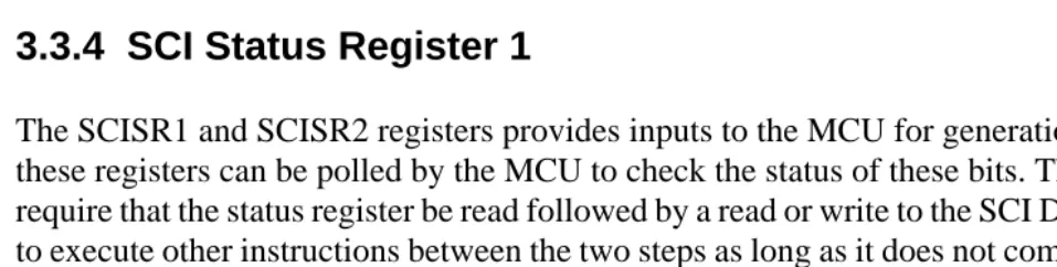
3.3.4 SCI Status Register 1
[image:18.792.63.542.581.702.2]The SCISR1 and SCISR2 registers provides inputs to the MCU for generation of SCI interrupts. Also, these registers can be polled by the MCU to check the status of these bits. The flag-clearing procedures require that the status register be read followed by a read or write to the SCI Data Register.It is permissible to execute other instructions between the two steps as long as it does not compromise the handling of I/O, but the order of operations is important for flag clearing.
Figure 3-5 SCI Status Register 1 (SCISR1)
Register address: $_4
7 6 5 4 3 2 1 0
R TDRE TC RDRF IDLE OR NF FE PF
W
RESET: 1 1 0 0 0 0 0 0
Read: anytime
Write: has no meaning or effect
TDRE — Transmit Data Register Empty Flag
TDRE is set when the transmit shift register receives a byte from the SCI data register. When TDRE is 1, the transmit data register (SCIDRH/L) is empty and can receive a new value to transmit.Clear TDRE by reading SCI status register 1 (SCISR1), with TDRE set and then writing to SCI data register low (SCIDRL).
1 = Byte transferred to transmit shift register; transmit data register empty 0 = No byte transferred to transmit shift register
TC — Transmit Complete Flag
TC is set low when there is a transmission in progress or when a preamble or break character is loaded. TC is set high when the TDRE flag is set and no data, preamble, or break character is being
transmitted.When TC is set, the TXD out signal becomes idle (logic 1). Clear TC by reading SCI status register 1 (SCISR1) with TC set and then writing to SCI data register low (SCIDRL). TC is cleared automatically when data, preamble, or break is queued and ready to be sent. TC is cleared in the event of a simultaneous set and clear of the TC flag (transmission not complete).
1 = No transmission in progress 0 = Transmission in progress
RDRF — Receive Data Register Full Flag
RDRF is set when the data in the receive shift register transfers to the SCI data register. Clear RDRF by reading SCI status register 1 (SCISR1) with RDRF set and then reading SCI data register low (SCIDRL).
1 = Received data available in SCI data register 0 = Data not available in SCI data register
IDLE — Idle Line Flag
IDLE is set when 10 consecutive logic 1s (if M=0) or 11 consecutive logic 1s (if M=1) appear on the receiver input. Once the IDLE flag is cleared, a valid frame must again set the RDRF flag before an idle condition can set the IDLE flag.Clear IDLE by reading SCI status register 1 (SCISR1) with IDLE set and then reading SCI data register low (SCIDRL).
1 = Receiver input has become idle
0 = Receiver input is either active now or has never become active since the IDLE flag was last cleared
NOTE: When the receiver wakeup bit (RWU) is set, an idle line condition does not set the IDLE flag.
OR is set when software fails to read the SCI data register before the receive shift register receives the next frame. The OR bit is set immediately after the stop bit has been completely received for the second frame. The data in the shift register is lost, but the data already in the SCI data registers is not affected. Clear OR by reading SCI status register 1 (SCISR1) with OR set and then reading SCI data register low (SCIDRL).
1 = Overrun 0 = No overrun
NOTE: OR flag may read back as set when RDRF flag is clear. This may happen if the following sequence of events occurs:
1. After the first frame is received, read status register SCISR1 (returns RDRF set and OR flag clear);
2. Receive second frame without reading the first frame in the data register (the second frame is not received and OR flag is set);
3. Read data register SCIDRL(returns first frame and clears RDRF flag in the status register);
4. read status register SCISR1 (returns RDRF clear and OR set).
Event 3 may be at exactly the same time as event 2 or any time after. When this happens, a dummy SCIDRL read following event 4 will be required to clear the OR flag if further frames are to be received.
NF — Noise Flag
NF is set when the SCI detects noise on the receiver input. NF bit is set during the same cycle as the RDRF flag but does not get set in the case of an overrun. Clear NF by reading SCI status register 1(SCISR1), and then reading SCI data register low (SCIDRL).
1 = Noise 0 = No noise
FE — Framing Error Flag
FE is set when a logic 0 is accepted as the stop bit. FE bit is set during the same cycle as the RDRF flag but does not get set in the case of an overrun. FE inhibits further data reception until it is cleared. Clear FE by reading SCI status register 1 (SCISR1) with FE set and then reading the SCI data register low (SCIDRL).
1 = Framing error 0 = No framing error
PF — Parity Error Flag
PF is set when the parity enable bit (PE) is set and the parity of the received data does not match the parity type bit(PT). PF bit is set during the same cycle as the RDRF flag but does not get set in the case of an overrun. Clear PF by reading SCI status register 1 (SCISR1), and then reading SCI data register low (SCIDRL).
0 = No parity error
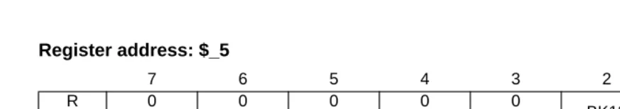
[image:21.792.89.526.130.207.2]3.3.5 SCI Status Register 2
Figure 3-6 SCI Status Register 2 (SCISR2)
Read: anytime
Write: anytime; writing accesses SCI status register 2; writing to any bits except TXDIR and BRK13 (SCISR2[1] & [2]) has no effect
BRK13 — Break Transmit character length
This bit determines whether the transmit break character is 10 or 11 bit respectively 13 or 14 bits long. The detection of a framing error is not affected by this bit.
1 = Break character is 13 or 14 bit long 0 = Break Character is 10 or 11 bit long
TXDIR — Transmitter pin data direction in Single-Wire mode.
This bit determines whether the TXD pin is going to be used as an input or output, in the Single-Wire mode of operation. This bit is only relevant in the Single-Wire mode of operation.
1 = TXD pin to be used as an output in Single-Wire mode 0 = TXD pin to be used as an input in Single-Wire mode
RAF — Receiver Active Flag
RAF is set when the receiver detects a logic 0 during the RT1 time period of the start bit search. RAF is cleared when the receiver detects an idle character.
1 = Reception in progress 0 = No reception in progress
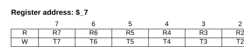
3.3.6 SCI Data Registers
Register address: $_5
7 6 5 4 3 2 1 0
R 0 0 0 0 0
BK13 TXDIR RAF W
RESET: 0 0 0 0 0 0 0 0
= Unimplemented or Reserved
Register address: $_6
7 6 5 4 3 2 1 0
R R8
T8 0 0 0 0 0 0
W
RESET: 0 0 0 0 0 0 0 0
Figure 3-7 SCI Data Registers (SCIDRH/L)
Read: anytime; reading accesses SCI receive data register
Write: anytime; writing accesses SCI transmit data register; writing to R8 has no effect
R8 — Received Bit 8
R8 is the ninth data bit received when the SCI is configured for 9-bit data format (M = 1).
T8 — Transmit Bit 8
T8 is the ninth data bit transmitted when the SCI is configured for 9-bit data format (M = 1).
R7-R0 — Received bits seven through zero for 9-bit or 8-bit data formats
T7-T0 — Transmit bits seven through zero for 9-bit or 8-bit formats
NOTE: If the value of T8 is the same as in the previous transmission, T8 does not have to be rewritten.The same value is transmitted until T8 is rewritten
NOTE: In 8-bit data format, only SCI data register low (SCIDRL) needs to be accessed.
NOTE: When transmitting in 9-bit data format and using 8-bit write instructions, write first to SCI data register high (SCIDRH), then SCIDRL.
Section 4 Functional Description
4.1 General
This section provides a complete functional description of the SCI block, detailing the operation of the design from the end user perspective in a number of subsections.
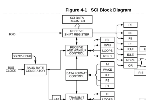
Figure 4-1 shows the structure of the SCI module. The SCI allows full duplex, asynchronous, NRZ serial communication between the CPU and remote devices, including other CPUs. The SCI transmitter and receiver operate independently, although they use the same baud rate generator. The CPU monitors the status of the SCI, writes the data to be transmitted, and processes received data.
Register address: $_7
7 6 5 4 3 2 1 0
R R7 R6 R5 R4 R3 R2 R1 R0
W T7 T6 T5 T4 T3 T2 T1 T0
RESET: 0 0 0 0 0 0 0 0
Figure 4-1 SCI Block Diagram
4.2 Data Format
The SCI uses the standard NRZ mark/space data format illustrated inFigure 4-2
below. SCI DATA RECEIVE SHIFT REGISTER SCI DATA REGISTER TRANSMIT SHIFT REGISTER REGISTER BAUD RATE GENERATOR SBR12–SBR0 BUS TRANSMIT CONTROL ÷16 RECEIVE AND WAKEUP DATA FORMAT CONTROL CONTROL T8 PF FE NF RDRF IDLE TIE OR TCIE TDRE TC R8 RAF LOOPS RWU RE PE ILT PT WAKE M CLOCK ILIE RIE RXD RSRC SBK LOOPS TE RSRC TXD RDRF/OR IRQ TDRE IRQ IDLE IRQ TC IRQ IRQ TO CPU BIT 5 START
BIT BIT 0 BIT 1
NEXT STOP
BIT
START BIT
9-BIT DATA FORMAT
BIT 2 BIT 3 BIT 4 BIT 6 BIT 7
PARITY OR DATA BIT PARITY OR DATA BIT
BIT M IN SCICR1 SET 8-BIT DATA FORMAT BIT M IN SCICR1 CLEAR
BIT 5
Figure 4-2 SCI Data Formats
Each data character is contained in a frame that includes a start bit, eight or nine data bits, and a stop bit. Clearing the M bit in SCI control register 1 configures the SCI for 8-bit data characters.A frame with eight data bits has a total of 10 bits. Setting the M bit configures the SCI for nine-bit data characters. A frame with nine data bits has a total of 11 bits
[image:24.792.187.428.285.395.2]When the SCI is configured for 9-bit data characters, the ninth data bit is the T8 bit in SCI data register high (SCIDRH). It remains unchanged after transmission and can be used repeatedly without rewriting it. A frame with nine data bits has a total of 11 bits.
Table 4-2 Example of 9-Bit Data Formats
4.3 Baud Rate Generation
A 13-bit modulus counter in the baud rate generator derives the baud rate for both the receiver and the transmitter. The value from 0 to 8191 written to the SBR12–SBR0 bits determines the module clock divisor. The SBR bits are in the SCI baud rate registers (SCIBDH and SCIBDL). The baud rate clock is synchronized with the bus clock and drives the receiver. The baud rate clock divided by 16 drives the transmitter. The receiver has an acquisition rate of 16 samples per bit time.
Table 4-1 Example of 8-bit Data Formats
Start Bit Data Bits Address Bits Parity Bits Stop Bit
1 8 0 0 1
1 7 0 1 1
1 7 11
NOTES:
1. The address bit identifies the frame as an address character. See section on Receiver Wakeup
0 1 Start Bit Data Bits Address Bits Parity Bits Stop Bit
1 9 0 0 1
1 8 0 1 1
1 8 11
NOTES:
1. The address bit identifies the frame as an address character. See section on Receiver Wakeup
[image:24.792.187.427.456.559.2]Baud rate generation is subject to one source of error:
[image:25.792.160.455.156.326.2]• Integer division of the module clock may not give the exact target frequency.
Table 4-3 lists some examples of achieving target baud rates with a module clock frequency of 25MHz
SCI baud rate = SCI module clock / (16 * SCIBR[12:0]
Table 4-3 Baud Rates (Example: Module Clock = 25MHz)
Bits SBR[12-0]
Receiver Clock (Hz)
Transmitter Clock (Hz)
Target Baud Rate
Error (%) 41 609,756.1 38,109.8 38,400 .76 81 308,642.0 19,290.1 19,200 .47 163 153,374.2 9585.9 9600 .16 326 76,687.1 4792.9 4800 .15 651 38,402.5 2400.2 2400 .01 1302 19,201.2 1200.1 1200 .01
2604 9600.6 600.0 600 .00
5208 4800.0 300.0 300 .00
10417 2400.0 150.0 150 .00
4.4 Transmitter
Figure 4-3 Transmitter Block Diagram
4.4.1 Transmitter Character Length
The SCI transmitter can accommodate either 8-bit or 9-bit data characters. The state of the M bit in SCI control register 1 (SCICR1) determines the length of data characters. When transmitting 9-bit data, bit T8 in SCI data register high (SCIDRH) is the ninth bit (bit 8).
4.4.2 Character Transmission
To transmit data, the MCU writes the data bits to the SCI data registers (SCIDRH/SCIDRL), which in turn are transferred to the transmitter shift register. The transmit shift register then shifts a frame out through the Tx output signal, after it has prefaced them with a start bit and appended them with a stop bit. The SCI
PE PT
H 8 7 6 5 4 3 2 1 0 L 11-BIT TRANSMIT SHIFT REGISTER
STOP START
T8
TDRE TIE
TCIE
SBK
TC PARITY
GENERATION
MSB
SCI DATA REGISTERS
LOAD FROM SCIDR SHIFT ENABLE PREAMBLE (ALL ONES) BREAK (ALL 0s)
TRANSMITTER CONTROL M
INTERNAL BUS
SBR12–SBR0
BAUD DIVIDER ÷16
TDRE INTERRUPT REQUEST
TC INTERRUPT REQUEST BUS
LOOP
RSRC CLOCK
TE
TO
CONTROL RXD
data registers (SCIDRH and SCIDRL) are the write-only buffers between the internal data bus and the transmit shift register.
The SCI also sets a flag, the transmit data register empty flag (TDRE), every time it transfers data from the buffer (SCIDRH/L) to the transmitter shift register.The transmit driver routine may respond to this flag by writing another byte to the Transmitter buffer (SCIDRH/SCIDRL), while the shift register is still shifting out the first byte.
To initiate an SCI transmission:
1. Configure the SCI:
a. Select a baud rate. Write this value to the SCI baud registers (SCIBDH/L) to begin the baud rate generator. Remember that the baud rate generator is disabled when the baud rate is zero. Writing to the SCIBDH has no effect without also writing to SCIBDL.
b. Write to SCICR1 to configure word length, parity, and other configuration bits (LOOPS,RSRC,M,WAKE,ILT,PE,PT).
c. Enable the transmitter, interrupts, receive, and wake up as required, by writing to the SCICR2 register bits (TIE,TCIE,RIE,ILIE,TE,RE,RWU,SBK). A preamble or idle character will now be shifted out of the transmitter shift register.
2. Transmit Procedure for Each Byte:
a. Poll the TDRE flag by reading the SCISR1 or responding to the TDRE interrupt. Keep in mind that the TDRE bit resets to one.
b. If the TDRE flag is set, write the data to be transmitted to SCIDRH/L, where the ninth bit is written to the T8 bit in SCIDRH if the SCI is in 9-bit data format. A new transmission will not result until the TDRE flag has been cleared.
3. Repeat step 2 for each subsequent transmission.
NOTE: The TDRE flag is set when the shift register is loaded with the next data to be transmitted from SCIDRH/L, which happens, generally speaking, a little over half-way through the stop bit of the previous frame. Specifically, this transfer occurs 9/16ths of a bit time AFTER the start of the stop bit of the previous frame.
Writing the TE bit from 0 to a 1 automatically loads the transmit shift register with a preamble of 10 logic 1s (if M = 0) or 11 logic 1s (if M = 1). After the preamble shifts out, control logic transfers the data from the SCI data register into the transmit shift register. A logic 0 start bit automatically goes into the least significant bit position of the transmit shift register. A logic 1 stop bit goes into the most significant bit position.
Hardware supports odd or even parity. When parity is enabled, the most significant bit (msb) of the data character is the parity bit.
When the transmit shift register is not transmitting a frame, the Tx output signal goes to the idle condition, logic 1. If at any time software clears the TE bit in SCI control register 2 (SCICR2), the transmitter enable signal goes low and the transmit signal goes idle.
If software clears TE while a transmission is in progress (TC = 0), the frame in the transmit shift register continues to shift out. To avoid accidentally cutting off the last frame in a message, always wait for TDRE to go high after the last frame before clearing TE.
To separate messages with preambles with minimum idle line time, use this sequence between messages:
1. Write the last byte of the first message to SCIDRH/L.
2. Wait for the TDRE flag to go high, indicating the transfer of the last frame to the transmit shift register.
3. Queue a preamble by clearing and then setting the TE bit.
4. Write the first byte of the second message to SCIDRH/L.
4.4.3 Break Characters
Writing a logic 1 to the send break bit, SBK, in SCI control register 2 (SCICR2) loads the transmit shift register with a break character. A break character contains all logic 0s and has no start, stop, or parity bit. Break character length depends on the M bit in SCI control register 1 (SCICR1). As long as SBK is at logic 1, transmitter logic continuously loads break characters into the transmit shift register. After software clears the SBK bit, the shift register finishes transmitting the last break character and then transmits at least one logic 1. The automatic logic 1 at the end of a break character guarantees the recognition of the start bit of the next frame.
The SCI recognizes a break character when a start bit is followed by eight or nine logic 0 data bits and a logic 0 where the stop bit should be. Receiving a break character has these effects on SCI registers:
• Sets the framing error flag, FE
• Sets the receive data register full flag, RDRF
• Clears the SCI data registers (SCIDRH/L)
• May set the overrun flag, OR, noise flag, NF, parity error flag, PE, or the receiver active flag, RAF (see 3.4.4 and 3.4.5 SCI Status Register 1 and 2)
4.4.4 Idle Characters
An idle character contains all logic 1s and has no start, stop, or parity bit. Idle character length depends on the M bit in SCI control register 1 (SCICR1). The preamble is a synchronizing idle character that begins the first transmission initiated after writing the TE bit from 0 to 1.
NOTE: When queueing an idle character, return the TE bit to logic 1 before the stop bit of the current frame shifts out through the Tx output signal. Setting TE after the stop bit appears on Tx output signal causes data previously written to the SCI data register to be lost. Toggle the TE bit for a queued idle character while the TDRE flag is set and immediately before writing the next byte to the SCI data register.
NOTE: If the TE bit is clear and the transmission is complete, the SCI is not the master of the TXD pin
[image:29.792.70.554.242.572.2]4.5 Receiver
Figure 4-4 SCI Receiver Block Diagram
ALL ONES M WAKE ILT PE PT RE
H 8 7 6 5 4 3 2 1 0 L 11-BIT RECEIVE SHIFT REGISTER
STOP START DATA WAKEUP PARITY CHECKING MSB
SCI DATA REGISTER
R8 RIE ILIE RWU RDRF OR NF FE PE INTERNAL BUS BUS
IDLE INTERRUPT REQUEST
4.5.1 Receiver Character Length
The SCI receiver can accommodate either 8-bit or 9-bit data characters. The state of the M bit in SCI control register 1 (SCICR1) determines the length of data characters. When receiving 9-bit data, bit R8 in SCI data register high (SCIDRH) is the ninth bit (bit 8).
4.5.2 Character Reception
During an SCI reception, the receive shift register shifts a frame in from the Rx input signal. The SCI data register is the read-only buffer between the internal data bus and the receive shift register.
After a complete frame shifts into the receive shift register, the data portion of the frame transfers to the SCI data register. The receive data register full flag, RDRF, in SCI status register 1 (SCISR1) becomes set, indicating that the received byte can be read. If the receive interrupt enable bit, RIE, in SCI control register 2 (SCICR2) is also set, the RDRF flag generates an RDRF interrupt request.
4.5.3 Data Sampling
The receiver samples the Rx input signal at the RT clock rate. The RT clock is an internal signal with a frequency 16 times the baud rate. To adjust for baud rate mismatch, the RT clock (seeFigure 4-5) is re-synchronized:
• After every start bit
• After the receiver detects a data bit change from logic 1 to logic 0 (after the majority of data bit samples at RT8, RT9, and RT10 returns a valid logic 1 and the majority of the next RT8, RT9, and RT10 samples returns a valid logic 0)
[image:30.792.57.552.482.689.2]To locate the start bit, data recovery logic does an asynchronous search for a logic 0 preceded by three logic 1s.When the falling edge of a possible start bit occurs, the RT clock begins to count to 16.
Figure 4-5 Receiver Data Sampling
RESET RT CLOCK
RT1 RT1 RT1 RT1 RT1 RT1 RT1 RT1 RT1 RT2 RT3 RT4 RT5 RT6 RT7 RT8
RT11
RT10
RT9
RT15
RT14
RT13
RT12 RT16 RT1 RT2 RT3 RT4
SAMPLES
RT CLOCK
RT CLOCK COUNT
START BIT Rx Input Signal
START BIT QUALIFICATION
START BIT DATA SAMPLING 1 1 1 1 1 1 1 1 0 0 0 0 0 0 0
LSB
To verify the start bit and to detect noise, data recovery logic takes samples at RT3, RT5, and RT7.Table 4-4 summarizes the results of the start bit verification samples.
Table 4-4 Start Bit Verification
If start bit verification is not successful, the RT clock is reset and a new search for a start bit begins.
[image:31.792.132.480.326.467.2]To determine the value of a data bit and to detect noise, recovery logic takes samples at RT8, RT9, and RT10.Table 4-5 summarizes the results of the data bit samples.
Table 4-5 Data Bit Recovery
NOTE: The RT8, RT9, and RT10 samples do not affect start bit verification. If any or all of the RT8, RT9, and RT10 start bit samples are logic 1s following a successful start bit verification, the noise flag (NF) is set and the receiver assumes that the bit is a start bit (logic 0).
To verify a stop bit and to detect noise, recovery logic takes samples at RT8, RT9, and RT10.Table 4-6
[image:31.792.129.523.580.698.2]summarizes the results of the stop bit samples.
Table 4-6 Stop Bit Recovery
RT3, RT5, and RT7 Samples Start Bit Verification Noise Flag
000 Yes 0
001 Yes 1
010 Yes 1
011 No 0
100 Yes 1
101 No 0
110 No 0
111 No 0
RT8, RT9, and RT10 Samples Data Bit Determination Noise Flag
000 0 0
001 0 1
010 0 1
011 1 1
100 0 1
101 1 1
110 1 1
111 1 0
RT8, RT9, and RT10 Samples Framing Error Flag Noise Flag
000 1 0
001 1 1
010 1 1
011 0 1
100 1 1
InFigure 4-6the verification samples RT3 and RT5 determine that the first low detected was noise and not the beginning of a start bit. The RT clock is reset and the start bit search begins again. The noise flag is not set because the noise occurred before the start bit was found.
Figure 4-6 Start Bit Search Example 1
[image:32.792.68.551.431.617.2]InFigure 4-7, verification sample at RT3 is high. The RT3 sample sets the noise flag. Although the perceived bit time is misaligned, the data samples RT8, RT9, and RT10 are within the bit time and data recovery is successful.
Figure 4-7 Start Bit Search Example 2
InFigure 4-8, a large burst of noise is perceived as the beginning of a start bit, although the test sample at RT5 is high. The RT5 sample sets the noise flag. Although this is a worst-case misalignment of
110 0 1
111 0 0
RT8, RT9, and RT10 Samples Framing Error Flag Noise Flag
RESET RT CLOCK
RT1 RT1 RT1 RT1 RT2 RT3 RT4 RT5 RT1 RT1 RT2 RT3 RT4 RT5 RT6 RT7
RT10 RT9 RT8 RT14 RT13 RT12
RT11 RT15 RT16 RT1 RT2 RT3
SAMPLES
RT CLOCK RT CLOCK COUNT
START BIT Rx Input Signal
1 1 1 0 1 1 1 0 0 0 0 0
LSB
0 0
RESET RT CLOCK
RT1 RT1 RT1 RT1 RT1 RT1 RT2 RT3 RT4 RT5 RT6 RT7 RT8
RT11
RT10
RT9
RT14
RT13
RT12 RT15 RT16 RT1 RT2 RT3 RT4 RT5 RT6 RT7
SAMPLES
RT CLOCK
RT CLOCK COUNT
ACTUAL START BIT Rx Input Signal
1 1 1 1 1 1 0 0 0 0
LSB
0 0
perceived bit time, the data samples RT8, RT9, and RT10 are within the bit time and data recovery is successful.
[image:33.792.62.554.336.522.2]Figure 4-8 Start Bit Search Example 3
Figure 4-9shows the effect of noise early in the start bit time. Although this noise does not affect proper synchronization with the start bit time, it does set the noise flag.
Figure 4-9 Start Bit Search Example 4
Figure 4-10shows a burst of noise near the beginning of the start bit that resets the RT clock. The sample after the reset is low but is not preceded by three high samples that would qualify as a falling edge.
RESET RT CLOCK
RT1 RT1 RT1 RT1 RT2 RT3 RT4 RT5 RT6 RT7 RT8 RT9 RT10 RT11 RT12 RT13 RT14 RT15 RT16 RT1 RT2 RT3 RT4 RT5 RT6 RT7 RT8 RT9
SAMPLES
RT CLOCK
RT CLOCK COUNT
ACTUAL START BIT Rx input Signal
1 1 1 0 1 0 0 0 0
LSB
0
PERCEIVED START BIT
RESET RT CLOCK
RT1 RT1 RT1 RT1 RT1 RT1 RT1 RT1 RT1 RT1 RT2 RT3 RT4 RT5 RT6 RT7 RT8 RT9 RT10 RT11 RT12 RT13 RT14 RT15 RT16 RT1 RT2 RT3
SAMPLES
RT CLOCK
RT CLOCK COUNT
PERCEIVED AND ACTUAL START BIT Rx Input Signal
1 1 1 1 1 0 1 0
LSB
1
Depending on the timing of the start bit search and on the data, the frame may be missed entirely or it may set the framing error flag.
Figure 4-10 Start Bit Search Example 5
InFigure 4-11, a noise burst makes the majority of data samples RT8, RT9, and RT10 high. This sets the noise flag but does not reset the RT clock. In start bits only, the RT8, RT9, and RT10 data samples are ignored.
Figure 4-11 Start Bit Search Example 6
4.5.4 Framing Errors
If the data recovery logic does not detect a logic 1 where the stop bit should be in an incoming frame, it sets the framing error flag, FE, in SCI status register 1 (SCISR1). A break character also sets the FE flag because a break character has no stop bit. The FE flag is set at the same time that the RDRF flag is set.
4.5.5 Baud Rate Tolerance
A transmitting device may be operating at a baud rate below or above the receiver baud rate. Accumulated bit time misalignment can cause one of the three stop bit data samples (RT8, RT9, and RT10) to fall
RESET RT CLOCK
RT1 RT1 RT1 RT1 RT1 RT1 RT1 RT1 RT1 RT1 RT2 RT3 RT4 RT5 RT6 RT7 RT1 RT1 RT1 RT1 RT1 RT1 RT1 RT1 RT1 RT1 RT1 RT1
SAMPLES
RT CLOCK RT CLOCK COUNT
START BIT Rx Input Signal
1 1 1 1 1 0 0 1
LSB
1
1 1 1 1 0 0 0 0 0 0 0 0 NO START BIT FOUND
RESET RT CLOCK
RT1 RT1 RT1 RT1 RT1 RT1 RT1 RT1 RT1 RT1 RT2 RT3 RT4 RT5 RT6 RT7
RT10 RT9 RT8 RT14 RT13 RT12
RT11 RT15 RT16 RT1 RT2 RT3
SAMPLES
RT CLOCK
RT CLOCK COUNT
START BIT Rx Input Signal
1 1 1 1 1 0 0 0
LSB
1
[image:34.792.66.553.344.510.2]outside the actual stop bit.A noise error will occur if the RT8, RT9, and RT10 samples are not all the same logical values. A framing error will occur if the receiver clock is misaligned in such a way that the majority of the RT8, RT9, and RT10 stopbit samples are a logic zero.
As the receiver samples an incoming frame, it re-synchronizes the RT clock on any valid falling edge within the frame. Re synchronization within frames will correct a misalignment between transmitter bit times and receiver bit times.
[image:35.792.139.481.235.366.2]4.5.5.1 Slow Data Tolerance
Figure 4-12shows how much a slow received frame can be misaligned without causing a noise error or a framing error. The slow stop bit begins at RT8 instead of RT1 but arrives in time for the stop bit data samples at RT8, RT9, and RT10.
Figure 4-12 Slow Data
Let’s take RTr as receiver RT clock and RTt as transmitter RT clock.
For an 8-bit data character, it takes the receiver 9 bit times x 16 RTr cycles +7 RTr cycles =151 RTr cycles to start data sampling of the stop bit .
With the misaligned character shown inFigure 4-12, the receiver counts 151 RTr cycles at the point when the count of the transmitting device is 9 bit times x 16 RTt cycles = 144 RTt cycles.
The maximum percent difference between the receiver count and the transmitter count of a slow 8-bit data character with no errors is:
((151 - 144) / 151) x 100 = 4.63%
For a 9-bit data character, it takes the receiver 10 bit times x 16 RTr cycles + 7 RTr cycles = 167 RTr cycles to start data sampling of the stop bit.
With the misaligned character shown inFigure 4-12, the receiver counts 167 RTr cycles at the point when the count of the transmitting device is 10 bit times x 16 RTt cycles = 160 RTt cycles.
The maximum percent difference between the receiver count and the transmitter count of a slow 9-bit character with no errors is:
((167 - 160) / 167) X 100 = 4.19%
MSB STOP
RT1 RT2 RT3 RT4 RT5 RT6 RT7 RT8 RT9 RT10 RT11 RT12 RT13 RT14 RT15 RT16
DATA SAMPLES RECEIVER
4.5.5.2 Fast Data Tolerance
Figure 4-13 shows how much a fast received frame can be misaligned. The fast stop bit ends at RT10 instead of RT16 but is still sampled at RT8, RT9, and RT10.
Figure 4-13 Fast Data
For an 8-bit data character, it takes the receiver 9 bit times x 16 RTr cycles + 10 RTr cycles = 154 RTr cycles to finish data sampling of the stop bit.
With the misaligned character shown inFigure 4-13, the receiver counts 154 RTr cycles at the point when the count of the transmitting device is 10 bit times x 16 RTt cycles = 160 RTt cycles.
The maximum percent difference between the receiver count and the transmitter count of a fast 8-bit character with no errors is:
((160 - 154) / 160) x 100 = 3.75%
For a 9-bit data character, it takes the receiver 10 bit times x 16 RTr cycles + 10 RTr cycles = 170 RTr cycles to finish data sampling of the stop bit.
With the misaligned character shown inFigure 4-13 , the receiver counts 170 RTr cycles at the point when the count of the transmitting device is 11 bit times x 16 RTt cycles = 176 RTt cycles.
The maximum percent difference between the receiver count and the transmitter count of a fast 9-bit character with no errors is:
((176 - 170) / 176) x 100 = 3.40%
4.5.6 Receiver Wakeup
To enable the SCI to ignore transmissions intended only for other receivers in multiple-receiver systems, the receiver can be put into a standby state. Setting the receiver wakeup bit, RWU, in SCI control register 2 (SCICR2) puts the receiver into standby state during which receiver interrupts are disabled.The SCI will still load the receive data into the SCIDRH/L registers, but it will not set the RDRF flag.
The transmitting device can address messages to selected receivers by including addressing information in the initial frame or frames of each message.
The WAKE bit in SCI control register 1 (SCICR1) determines how the SCI is brought out of the standby state to process an incoming message. The WAKE bit enables either idle line wakeup or address mark wakeup.
IDLE OR NEXT FRAME STOP
RT1 RT2 RT3 RT4 RT5 RT6 RT7 RT8 RT9 RT10 RT11 RT12 RT13 RT14 RT15 RT16
DATA SAMPLES RECEIVER
4.5.6.1 Idle input line wakeup (WAKE = 0)
In this wakeup method, an idle condition on the Rx Input signal clears the RWU bit and wakes up the SCI. The initial frame or frames of every message contain addressing information. All receivers evaluate the addressing information, and receivers for which the message is addressed process the frames that follow. Any receiver for which a message is not addressed can set its RWU bit and return to the standby state. The RWU bit remains set and the receiver remains on standby until another idle character appears on the Rx
Input signal.
Idle line wakeup requires that messages be separated by at least one idle character and that no message contains idle characters.
The idle character that wakes a receiver does not set the receiver idle bit, IDLE, or the receive data register full flag, RDRF.
The idle line type bit, ILT, determines whether the receiver begins counting logic 1s as idle character bits after the start bit or after the stop bit. ILT is in SCI control register 1 (SCICR1).
4.5.6.2 Address mark wakeup (WAKE = 1)
In this wakeup method, a logic 1 in the most significant bit (msb) position of a frame clears the RWU bit and wakes up the SCI. The logic 1 in the msb position marks a frame as an address frame that contains addressing information. All receivers evaluate the addressing information, and the receivers for which the message is addressed process the frames that follow.Any receiver for which a message is not addressed can set its RWU bit and return to the standby state. The RWU bit remains set and the receiver remains on standby until another address frame appears on the Rx Input signal.
The logic 1 msb of an address frame clears the receiver’s RWU bit before the stop bit is received and sets the RDRF flag.
Address mark wakeup allows messages to contain idle characters but requires that the msb be reserved for use in address frames.{sci_wake}
NOTE: With the WAKE bit clear, setting the RWU bit after the Rx Input signal has been idle can cause the receiver to wake up immediately.
4.6 Single-Wire Operation
Figure 4-14 Single-Wire Operation (LOOPS = 1, RSRC = 1)
Enable single-wire operation by setting the LOOPS bit and the receiver source bit, RSRC, in SCI control register 1 (SCICR1). {sci_single}Setting the LOOPS bit disables the path from the Rx Input signal to the receiver. Setting the RSRC bit connects the receiver input to the output of the TXD pin driver.{sci_single} Both the transmitter and receiver must be enabled (TE=1 and RE=1).The TXDIR bit (SCISR2[1]) determines whether the TXD pin is going to be used as an input (TXDIR = 0) or an output (TXDIR = 1) in this mode of operation.
4.7 Loop Operation
In loop operation the transmitter output goes to the receiver input. The Rx Input signal is disconnected from the SCI
.
Figure 4-15 Loop Operation (LOOPS = 1, RSRC = 0)
Enable loop operation by setting the LOOPS bit and clearing the RSRC bit in SCI control register 1 (SCICR1). Setting the LOOPS bit disables the path from the Rx Input signal to the receiver. Clearing the RSRC bit connects the transmitter output to the receiver input. Both the transmitter and receiver must be enabled (TE = 1 and RE = 1).
Section 5 Initialization/Application Information
RXD TRANSMITTER
RECEIVER
Tx Output Signal Tx Input Signal
RXD TRANSMITTER
RECEIVER
[image:38.792.185.437.413.485.2]5.1 Reset Initialization
The reset state of each individual bit is listed within the Register Description section (see Section 3
Memory Map and Register Definition) which details the registers and their bit-fields. All special
functions or modes which are initialized during or just following reset are described within this section.
5.2 Modes of Operation
5.2.1 Run Mode
Normal mode of operation.
5.2.2 Wait Mode
SCI operation in wait mode depends on the state of the SCISWAI bit in the SCI control register 1 (SCICR1).
• If SCISWAI is clear, the SCI operates normally when the CPU is in wait mode.
• If SCISWAI is set, SCI clock generation ceases and the SCI module enters a power-conservation state when the CPU is in wait mode. Setting SCISWAI does not affect the state of the receiver enable bit, RE, or the transmitter enable bit, TE.
If SCISWAI is set, any transmission or reception in progress stops at wait mode entry. The transmission or reception resumes when either an internal or external interrupt brings the CPU out of wait mode. Exiting wait mode by reset aborts any transmission or reception in progress and resets the SCI.
5.2.3 Stop Mode
The SCI is inactive during stop mode for reduced power consumption. The STOP instruction does not affect the SCI register states, but the SCI module clock will be disabled. The SCI operation resumes from where it left off after an external interrupt brings the CPU out of stop mode. Exiting stop mode by reset aborts any transmission or reception in progress and resets the SCI.
5.3 Interrupt Operation
5.3.1 System Level Interrupt Sources
There are five interrupt sources that can generate an SCI interrupt in to the CPU. They are listed inTable 5-1.
Table 5-1 SCI Interrupt Source
Interrupt
Source Flag
5.3.2 Interrupt Descriptions
The SCI only originates interrupt requests. The following is a description of how the SCI makes a request and how the MCU should acknowledge that request. The interrupt vector offset and interrupt number are chip dependent. The SCI only has a single interrupt line (SCI Interrupt Signal, active high operation) and all the following interrupts, when generated, are ORed together and issued through that port.
5.3.3 TDRE Description
The TDRE interrupt is set high by the SCI when the transmit shift register receives a byte from the SCI data register. A TDRE interrupt indicates that the transmit data register (SCIDRH/L) is empty and that a new byte can be written to the SCIDRH/L for transmission.Clear TDRE by reading SCI status register 1 with TDRE set and then writing to SCI data register low (SCIDRL).
5.3.4 TC Description
The TC interrupt is set by the SCI when a transmission has been completed.A TC interrupt indicates that there is no transmission in progress. TC is set high when the TDRE flag is set and no data, preamble, or break character is being transmitted. When TC is set, the TXD pin becomes idle (logic 1). Clear TC by reading SCI status register 1 (SCISR1) with TC set and then writing to SCI data register low (SCIDRL).TC is cleared automatically when data, preamble, or break is queued and ready to be sent.
5.3.5 RDRF Description
The RDRF interrupt is set when the data in the receive shift register transfers to the SCI data register. A RDRF interrupt indicates that the received data has been transferred to the SCI data register and that the byte can now be read by the MCU. The RDRF interrupt is cleared by reading the SCI status register one (SCISR1) and then reading SCI data register low (SCIDRL).
5.3.6 OR Description
The OR interrupt is set when software fails to read the SCI data register before the receive shift register receives the next frame. The newly acquired data in the shift register will be lost in this case, but the data already in the SCI data registers is not affected. The OR interrupt is cleared by reading the SCI status register one (SCISR1) and then reading SCI data register low (SCIDRL).
Transmitter TC TCIE Receiver RDRF RIE
OR
[image:40.792.222.390.70.155.2]Receiver IDLE ILIE
Table 5-1 SCI Interrupt Source
Interrupt
Source Flag
5.3.7 IDLE Description
The IDLE interrupt is set when 10 consecutive logic 1s (if M=0) or 11 consecutive logic 1s (if M=1) appear on the receiver input. Once the IDLE is cleared, a valid frame must again set the RDRF flag before an idle condition can set the IDLE flag. Clear IDLE by reading SCI status register 1 (SCISR1) with IDLE set and then reading SCI data register low (SCIDRL).
5.3.8 Recovery from Wait Mode
FINAL PAGE OF
45