Rutile TiO2 films as electron transport layer in inverted
organic solar cell
AL-HASHIMI, Mohammed K., KADEM, Burak Y. and HASSAN, Aseel K. <http://orcid.org/0000-0002-7891-8087>
Available from Sheffield Hallam University Research Archive (SHURA) at:
http://shura.shu.ac.uk/18582/
This document is the author deposited version. You are advised to consult the publisher's version if you wish to cite from it.
Published version
AL-HASHIMI, Mohammed K., KADEM, Burak Y. and HASSAN, Aseel K. (2018). Rutile TiO2 films as electron transport layer in inverted organic solar cell. Journal of Materials Science: Materials in Electronics, 29 (9), 7152-7160.
Copyright and re-use policy
See http://shura.shu.ac.uk/information.html
Sheffield Hallam University Research Archive
Rutile TiO
2films as electron transport layer in inverted organic solar cell
Mohammed K.Al-hashimia and Burak Y. Kadem*b and Aseel K. Hassanc
a
Mathematics department, Missan University, Iraq.
b
Physics department, College of Science, University of Babylon, Iraq.
c
Material and Engineering research institute , Sheffield Hallam University, UK
Abstract
Titanium dioxide (TiO2) thin films were prepared by sol–gel spin coating method and
deposited on ITO-coated glass substrates. The effects of different heat treatment annealing temperatures on the phase composition of TiO2 films and its effect on the optical band gap,
morphological, structural as well as using these layers in P3HT:PCBM-based organic solar cell were examined. The results show the presence of rutile phases in the TiO2 films which
were heat-treated for 2h at different temperatures (200oC, 300oC, 400oC, 500oC and 600oC). The optical properties of the TiO2 films have altered by temperature with a slight
decrease in the transmittance intensity in the visible region with increasing the temperature. The optical band gap values were found to be in the range of 3.28-3.59eV for the forbidden direct electronic transition and 3.40-3.79eV for the allowed direct transition. TiO2 layers were used as electron transport layer in inverted organic solar cells and
resulted in a power conversion efficiency of 1.59% with short circuit current density of 6.64mA.cm-2 for TiO2 layer heat-treated at 600oC.
1. Introduction
In the recent years, significant attention has been paid to the organic solar cells (OSCs) based on bulk-heterojunction (BHJ) materials, due to their low manufacturing cost and potential applications in the field of flexible and large-area solar cells [1]. It could be said that poly(3-hexylthiophene) (P3HT) and (6,6)-phenyl-C61 butyric acid methyl ester (PCBM) are considered as the most investigated materials for OSCs [2]. The inverted organic solar cells (IOSCs) exhibit competitive performance and offer better stability compared with the traditional OSCs [3]. The nature of the contacts on both sides of the active layer is considered as an essential feature to determine the OSCs parameters, hence the final power conversion efficiency (PCE) [4]. Titanium dioxide (TiO2) films are used in
phase is the most stable phase, however, the solution-based preparation methods for TiO2
generally shows the anatase phase [6]. Moreover, large anatase particles are difficult to synthesize, because of the transformation from anatase to rutile by increasing treatment times and/or temperature [7]. In an IOSC, a thin film of N-type metal oxide, such as titanium oxide (TiO2) is used as a cathode buffer layer in order to lower the work function
of the indium tin oxide (ITO) substrate. TiO2 is an attractive material due to its
non-toxicity, low cost, excellent stability, high electron mobility, and high transparency in the visible wavelength range [8]. Chen [9] have reviewed the basic synthetic methods of TiO2
nanomaterials and films such as sol-gel, hydrothermal, solvothermal and microwave methods. They have demonstrated that the sol-gel method is a versatile method which can produce even amorphous or low crystalline TiO2 films at low temperatures. Nevertheless,
the latter TiO2 structures could result in low electron mobility when using in the solar cells
applications and consequently result in poor device performance [10], thus, the use of heat treatment combined with sol-gel method is desired. There are several techniques that can be used to prepare TiO2 films such as sol–gel method which is believed to hold the greatest
potential for large-scale commercial [11]. PV performance is well-defined by its PCE which is determined by on several factors such as light harvesting and the exciton diffusion length, separation, transportation and collection by the selective electrodes in the solar cell [12]. Though, the adjustment of both contacts has shown to play significant role in the improvement of charge collection [13]. The heat treatment of TiO2 thin films is known as
one of the key factors to adjust the morphology; various TiO2 nanostructures films have
prepared by solution processing methods to acquire efficient charge transport layer [8, 14] as well as changing the structural and optical properties of the thin films [15, 16]. Mainly, Rutile Structure TiO2 is used in dye syntheses and perovskite solar cells [17-21]. In the
current study, the effects of heat treatment on the TiO2 thin film properties and employing
these films as electron transport layer in P3HT:PCBM-based inverted organic solar cells have been investigated. To the best of the authors’ knowledge, this is the first attempt to use rutile TiO2 structure with inverted OSC.
2. Samples preparation
2.1. Preparation of TiO2 films
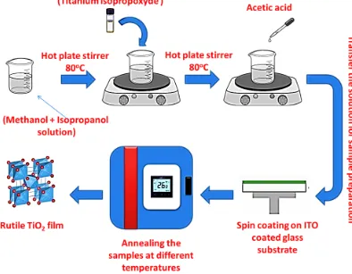
mixed together and used as solvents; Titanium isopropoxyde (TIP) with a purity of 97 % (Aldrich) (titanium precursor) was added to the solvents mixture under stirrer and temperature of 80oC. Afterward, acetic acid (which is act as catalyst, cathode buffer layer to modify the work function of ITO and as the electron transport layer (ETL) on ITO bottom electrode) was dropped wisely to the mixture under stirring. Fig.1 illustrates the steps of preparing Rutile TiO2. The latter layer was prepared by using sol-gel and spin
coating methods; the TiO2 thin films were spun with the spin speed of 2000rpm for 30sec,
(where the film thickness was estimated by ellipsometry is about 190nm), followed by heat treatment in a programmable furnace at 200 oC, 300 OC, 400 OC, 500 OC and 600 OC.
2.2. Preparation of OSCs
Chlorobenzene solution of poly (3- hexylthiophene) (P3HT) (Sigma-Aldrich) and [6,6]-phenyl C61-butyric acid methylester (PCBM) (Sigma-Aldrich) with a mixture ratio of 1:1 [22] was employed to prepare the active layer. This active layer was deposited by spin coating method onto the TiO2 layer (which was previously prepared onto ITO coated glass
substrates), followed by annealing at hot plate inside the nitrogen filled glove box at 120oC for 10min [23]. Hole transport layer consist of Poly(3,4ethylenedioxythiophene): poly(styrenesulfonate) (PEDOT:PSS) (Sigma-Aldrich) (conductive grade) is used; this layer was spun coated onto the active layer. Further heat treatment in the nitrogen-filled glove box at 110 OC was carried out for 10 min. A top contact of gold (Au) was then thermally evaporated with a thickness of 100 nm under vacuum of about10-6 mbar, at the deposition rate of 0.1-0.2nm.sec-1 (with the process monitored by a quartz crystal thickness monitor) onto the PEDOT:PSS layer surface. The schematic diagram of device under study is shown in Fig. 2.
2.3. Characterization
(SCS) and the photocurrent was generated under AM 1.5 solar simulator source of 100 mW.cm-2. The Fill factor (FF) and the PCE of the solar cells were evaluated using the following equations [24]:
PCE =JmaxVmax
Pin (1)
FF =JmaxVmax
JscVoc (2)
where Jsc is the short circuit current density (mA.cm-2 ), Voc is the open-circuit voltage (V),
Pin is the incident light power and Jmax (mA.cm-2 ) and Vmax (V) are the current density and
voltage at the point of maximum power output in the J-V curves [25].
3. Results and discussions:
3.1. Optical characteristics
The transmittance spectra of the studied TiO2 films under different heat-treatment
temperature are illustrated in Fig.3. Generally, TiO2 thin film is highly transparent in the
visible range 310–700nm. TiO2 film which was heat treated at 200oC has shown high
transmittance spectra in the range of wavelength from 750-400nm, which is useful for the solar cell applications; transmittance spectra shows a slight decrease by increasing of heat treatment. TiO2 thin film is well-known as a direct band gap transition semiconductor,
plots of the hυ2 vs the energy of the absorbed light affords the TiO2 band gap [26]. The
absorption coefficient (α) of TiO2 thin films were calculated from the optical transmittance
measurements using the following equation [27]:
α =2.303d × log (T1) (3)
where, T is the transmittance and d is the thickness of the TiO2 films. The absorption
coefficient can also be described as a function of incident photon energy (eV) to calculate the energy band gap (Eg) for the studied films using the following relation:
αhν = A(hν − Eg)n (4)
where, h is the Planck’s constant, υ is frequency, A is constant and n is a value depends on the nature of transition. Generally, the rutile TiO2 belongs to direct band gap
semiconductor category [28]. Therefore, when n= 1/2 the band gap transition is allowed direct and the extrapolation of the linear region of (αhυ)2
vs. hυ curve at α = 0 provides the direct energy band gap of TiO2 thin film [27]; whereas n= 3/2 the band gap transition is
the absorption of the P3HT main polymer while the band D is related to the absorption in the PCBM domains [29]. Fig.4 shows Tauc plot to determine the energy band gap for the studied TiO2 films. The energy gap values depend in general on the films crystal structure,
and the arrangement and distribution of the atoms in the crystal lattice. Also it is affected by crystal regularity [7]. The allowed direct band gap (Fig.4A) was found to be increase with increasing the temperature from 3.4eV (200oC) to 3.79eV (600oC). On the other hand, the forbidden direct band gap (Fig.4B) has increased from 3.28eV (200oC) to 3.59eV (600oC); the results are shown in table 1. Usually rutile phase has a band gap higher than
3eV, however the differences in our results have been correlated to the structure properties which lead to different electronic configuration; where the Ti-Ti and Ti-O distances in
TiO2 structure are different between anatase and rutile phase [30].
3.2. Structural properties
The structural properties of the TiO2 film were analyzed by X-ray diffraction as shown in
Fig.5. All the TiO2 films have exhibited polycrystalline structure; the TiO2 structure shows
no anatase phases, whereas clear peaks of Rutile phases have been observed at around 27o (110), 34o (101), 38o (200), 51o (211), 61o (002) and 66o (310) [31, 32]. The fine variation in the temperature has shown a slight increase in the intensity of XRD peaks and better crystallinity take place at higher temperature (600oC). In the XRD patterns, the (110) reflection appears anomalously intense indicating that the material is preferentially oriented [7]. Other diffraction peaks were observed at different phases, these are, (101, 200, 211, 002 and 310) which were attributed to the rutile phases of the TiO2 structure [7].
To determine the structure parameters, the main XRD peaks at 2Theta were fitted with one Gaussian to obtain the peaks’ width and the lattice constants as illustrated in Table 2. Moreover, the grain sizes (D) of the nanocrystalline structure for the studied TiO2 layers
were calculated using Scherer equation [29]:
D =β cos (θ)kλ (5)
where D is the grain size, λ is the wavelength of the radiation, k is called Scherrer’s constant which is equal to 0.94, β is the peak width at half-maximum intensity and θ is the peak position. From table 2, it is obvious that the crystal size of the TiO2 has increase upon
3.3. Morphological properties
The morphological properties of the studied TiO2 layer treated at different temperatures
were analyzed using SEM and AFM techniques. Fig.6 shows the SEM images for the TiO2
films with different heat-treatment temperatures. TiO2 surface morphology has exhibited a
clear porous nature; this morphology has changed upon increasing the heat-treatment temperature to 500oC and 600oC to become bigger grain size and more homogeneous surface morphology. The film heat treatment at 300, 400 and 500 oC showed some granular structures with irregular sizes. At 600oC heat treatment, the films exhibit irregular and grainier structure with no clear pinholes, which is in good agreement with XRD results for increasing the grain size with increasing temperature. The presence of pin holes usually decreases the efficiency of solar cells by shorting the back contact to the front Transparent Conducting Oxide (TCO) layer. These results confirm that heat treatment enhances the recrystallization and the grains became denser to fill the gaps and form a uniform thin layer of TiO2. Similar results have been observed from the AFM images as shown in Fig.7. The
topographic images have demonstrated that the grain size increases with the increasing of heat treatment temperature; the surface roughness (RMS) of the TiO2 films was estimated
for the studied films as (0.129nm ,0.273nm, 0.512nm, 0.610nm and 0.920nm) for the heat treatment temperatures 200oC, 300 oC, 400 oC, 500 oC and 600 oC, respectively.
3.4. Photovoltaic characteristics
The photovoltaic properties of the inverted organic solar cells based on P3HT:PCBM active layer using TiO2 as electron transport layer was investigated. Fig.8 and table 3 show
J-V characteristics of the (ITO/TiO2/P3HT:PCBM/PEDOT:PSS/Au) solar cells with
different heat treatment of TiO2 from (200-600 oC). Devices with TiO2 treated at higher
temperature have exhibited an increase in the short circuit density current (Jsc) from 1.06
mA.cm-2 to 6.64 mA.cm-2 and a slight increase in the open circuit voltage (Voc) from 0.59V
to 0.60V. The corresponding results show that the obtained solar cell with the TiO2 thin
film heat treatment of 600 oC has exhibited better photovoltaic properties, indicating that more electrons can be extracted and transported to ITO [33]. Moreover, PCE of the studied devices have revealed a clear increase in PCE from 0.35% in the device with TiO2 treated
at 200oC to 1.6% in the device with TiO2 treated at 600oC. However, the FF has shown a
This may be attributed to the increase in the series resistance [23]. The series resistance of the studied devices has shown an increase from 9.6(Ω.cm-2) in the device with TiO2 treated
with temperature at 200oC to 48.9(Ω.cm-2) in the device treated at 600oC. However, PCE for devices with an active area less than 0.1cm2 show slight sensitivity to the cathode conductivity [34]. Generally, two basic processes are controlled the J-V characteristics of OSCs: carrier injection in the bulk material by the electrodes and charge transport in the bulk material [35]. The carriers’ injection process is also governed by different processes: Schottky emission (thermionic emission), Poole–Frenkel emission (field-enhanced thermal excitation of trapped charges) and charge tunneling (Fowle–Nordheim tunneling from the metal contact into the HOMO and LUMO levels of the polymer) [36]. The injected carriers by the electrode have to overcome Schottky barrier or tunnel through it. After the carriers’ injection, the conduction properties of the active layer play the main role in transportation toward the opposite electrode. Mainly, Ohmic conduction is dominated in the charge carriers’ transportation in a bulk materials such as P3HT:PCBM at low voltages [37]. This could be attributed to the thermally excited carriers’ hopping between the isolated states and the space-charge-limited current (SCLC) is mostly due to carriers’ injection from the electrode to the active layer [38]. In the case of P3HT:PCBM-based organic solar cells, an interpenetrated percolation pathways is form to transport the charge carrier where the holes are transported through P3HT domains and electrons through the PCBM domains, which is limited by the charge carriers’ mobility [39]. Low charge carrier mobility in organic materials is mostly a function of ‘‘mobility gaps’’ due to the structural disorder [40]. Therefore, recombination is very likely to occur during the transport process, the total resistance will increase exponentially, which is due to the recombination effect [33], which in turn affects the FF.
Conclusion:
Titanium dioxide thin films were prepared using sol-gel process. XRD peaks were observed at different phases, these are, (101, 200, 211, 002 and 310) which were attributed to the rutile phases of the TiO2 structure. The latter structure belongs to direct band gap
semiconductor category. Using Tauc equation, the allowed direct band gap was found to be increase with increasing the temperature from 3.4eV (200oC) to 3.79eV (600oC) and the forbidden direct band gap has increased from 3.28eV (200oC) to 3.59eV (600oC). TiO2
and more homogeneous surface morphology. The PV properties have shown an increase after the thermal treatment of TiO2, FF has shown a clear reduction from 55.5% to 42.3% which could be due to the increase in the series resistance. PCE of 1.59% with high photo current density of 6.64mA.cm-2 using TiO2 layer heat-treated at 600oC has been achieved.
References
[1] Huang, H. L., Lee, C. T., & Lee, H. Y., Performance improvement mechanisms of P3HT: PCBM inverted polymer solar cells using extra PCBM and extra P3HT interfacial layers. Organic Electronics, 21(2015):126-131.
[2] Xu, Z. X., Roy, V. A. L., Low, K. H., & Che, C. M., Bulk heterojunction photovoltaic cells based on tetra-methyl substituted copper (II) phthalocyanine:P3HT:PCBM composite. Chemical communications, 47(2011), 9654-9656.
[3] Wang, J.C., Weng, W.T., Tsai, M.Y., Lee, M.K., Horng, S.F., Perng, T.P., Kei, C.C., Yu, C.C. and Meng, H.F., Highly efficient flexible inverted organic solar cells using atomic layer deposited ZnO as electron selective layer. Journal of Materials Chemistry, 20(2010):862-866.
[4] Kadem, B., Cranton, W., and Hassan, A., Metal salt modified PEDOT: PSS as anode buffer layer and its effect on power conversion efficiency of organic solar cells. Organic Electronics, 24 (2015):73-79.
[5] Chen, X. and Mao, S. S., Titanium dioxide nanomaterials: synthesis, properties, modifications, and applications. Chem. Rev, 107(2007):2891-2959.
[6] Zaban, A., Aruna, S. T., Tirosh, S., Gregg, B. A. and Mastai, Y., The effect of the preparation condition of TiO2 colloids on their surface structures. The Journal of Physical Chemistry B, 104(2000):4130-4133.
[7] Reyes-Coronado, D., Rodríguez-Gattorno, G., Espinosa-Pesqueira, M. E., Cab, C., de Coss, R. D. and Oskam, G., Phase-pure TiO2 nanoparticles: anatase, brookite and rutile. Nanotechnology, 19(2008):145605.
[8] Lin, Z., Jiang, C., Zhu, C. and Zhang, J., Development of inverted organic solar cells with TiO2 interface layer by using low-temperature atomic layer deposition. ACS applied materials & interfaces, 5(2013):713-718.
[9] Chen, X., & Mao, S. S., Titanium dioxide nanomaterials: synthesis, properties, modifications, and applications. Chem. Rev, 107(2007), 2891-2959.
[10] Hadipour, A., Cheyns, D., Heremans, P., & Rand, B. P., Electrode considerations for the optical enhancement of organic bulk heterojunction solar cells. Advanced energy materials, 1(2011), 930-935.
[11] Hau, S. K., Yip, H. L., Acton, O., Baek, N. S., Ma, H. and Jen, A. K. Y., Interfacial modification to improve inverted polymer solar cells. Journal of Materials Chemistry, 18(2008):5113-5119.
[12] Hsieh-Cheng Han, Chi-Ang Tseng, Chan-Yi Du, Abhijit Ganguly, Cheong-Wei Chong, Sheng-Bo Wang, Chi-Feng Lin, Sheng-Hsiung Chang, Chao-Chin Su, Jiun-Haw Lee, Kuei-Hsien Chen and Li-Chyong Chen, Enhancing efficiency with fluorinated interlayers in small molecule organic solar cells, J. Mater. Chem., 22 (2012):22899.
[13] R. Steim, F. R. Kogler and C. J. Brabec, Interface materials for organic solar cells, J. Mater. Chem., 20 (2010):2499.
Low-temperature processed electron collection layers of graphene/TiO2 nanocomposites in
thin film perovskite solar cells. Nano letters, 14(2013):724-730.
[15] Mor, G. K., Shankar, K., Paulose, M., Varghese, O. K., & Grimes, C. A., Use of highly-ordered TiO2 nanotube arrays in dye-sensitized solar cells. Nano
letters, 6(2006):215-218.
[16] Zhang, D., Xie, F., Lin, P. and Choy, W. C., Al-TiO2 composite-modified
single-layer graphene as an efficient transparent cathode for organic solar cells. ACS nano, 7(2013):1740-1747.
[17] Sommeling, P.M., O'regan, B.C., Haswell, R.R., Smit, H.J.P., Bakker, N.J., Smits, J.J.T., Kroon, J.M. and Van Roosmalen, J.A.M, Influence of a TiCl4 post-treatment on nanocrystalline TiO2 films in dye-sensitized solar cells. The Journal of Physical Chemistry B, 110(2006):19191-19197.
[18] Chen, Q., Zhou, H., Hong, Z., Luo, S., Duan, H.S., Wang, H.H., Liu, Y., Li, G. and Yang, Planar heterojunction perovskite solar cells via vapor-assisted solution process. Journal of the American Chemical Society, 136(2013):622-625.
[19] Van de Lagemaat, J. and Frank, A. J., Effect of the surface-state distribution on electron transport in dye-sensitized TiO2 solar cells: Nonlinear electron-transport
kinetics. The Journal of Physical Chemistry B, 104(2000):4292-4294.
[20] Ekar, S.U., Shekhar, G., Khollam, Y.B., Wani, P.N., Jadkar, S.R., Naushad, M., Chaskar, M.G., Jadhav, S.S., Fadel, A., Jadhav, V.V. and Shendkar, J.H, Green synthesis and dye-sensitized solar cell application of rutile and anatase TiO2
nanorods. Journal of Solid State Electrochemistry, 21(2017):2713-2718.
[21] Hu, J., Liu, P., Chen, M., Li, S. and Yang, Y., Synthesis and First-principle Calculation of TiO2 Rutile Nanowire Electrodes for Dye-sensitized Solar Cells. Int. J. Electrochem. Sci, 12(2017):9725-9735.
[22] Kadem, B. Y., Hassan, A. K. and Cranton, W., Enhancement of power conversion efficiency of P3HT: PCBM solar cell using solution processed Alq3 film as electron transport layer. Journal of Materials Science: Materials in Electronics, 26(2015):3976-3983.
[23] Kadem, B., Hassan, A. and Cranton, W., Efficient P3HT: PCBM bulk heterojunction organic solar cells; effect of post deposition thermal treatment. Journal of Materials Science: Materials in Electronics, 27(2016):7038-7048.
[24] G.T. Yue, J.H. Wu, Y.M. Xiao, H.F. Ye, J.M. Lin and M.L. Huang, Flexible dye-sensitized solar cell based on PCBM/P3HT hetrojunction. Chin. Sci. Bull. 56(2011):325–330.
[25] Kadem, B. and Hassan, A., The effect of fullerene derivatives ratio on P3HT-based organic solar cells. Energy Procedia, 74(2015):439-445.
[26] Wang, Y., Zhang, L., Deng, K., Chen, X. and Zou, Z., Low temperature synthesis and photocatalytic activity of rutile TiO2 nanorod superstructures. The Journal of Physical Chemistry C, 111(2007):2709-2714.
[28] Zhang, J., Zhou, P., Liu, J. and Yu, J., New understanding of the difference of photocatalytic activity among anatase, rutile and brookite TiO2. Physical Chemistry
Chemical Physics, 16(2014):20382-20386.
[29] Kadem, B. Y., Al-hashimi, M. K. and Hassan, A. K., The effect of solution processing on the power conversion efficiency of P3HT-based organic solar cells. Energy Procedia, 50(2014):237-245.
[30] Landmann, M., Rauls, E. and Schmidt, W.G., The electronic structure and optical response of rutile, anatase and brookite TiO2. Journal of physics: condensed
matter, 24(2012):195503.
[31] Thamaphat, K., Limsuwan, P. and Ngotawornchai, B., Phase characterization of TiO2 powder by XRD and TEM. Kasetsart J.(Nat. Sci.), 42(2008):357-361.
[32] Kumar, A., Madaria, A. R. and Zhou, C., Growth of aligned single-crystalline rutile TiO2 nanowires on arbitrary substrates and their application in dye-sensitized solar cells. The Journal of Physical Chemistry C, 114(2010):7787-7792.
[33] Zhu, L., Lu, Q., Lv, L., Wang, Y., Hu, Y., Deng, Z., Lou, Z., Hou, Y. and Teng, F. (2017), Ligand-free rutile and anatase TiO 2 nanocrystals as electron extraction layers for high performance inverted polymer solar cells. RSC Advances, 7(33), 20084-20092.
[34] Servaites, J. D., Ratner, M. A. and Marks, T. J., Organic solar cells: a new look at traditional models. Energy & Environmental Science, 4(2011):4410-4422.
[35] S.M. Sze, Semiconductor Devices Physics and Technology, 2nd ed., Wiley, New York, 2001.
[36] Shen, Y., Li, K., Majumdar, N., Campbell, J. C. and Gupta, M. C., Bulk and contact resistance in P3HT: PCBM heterojunction solar cells. Solar Energy Materials and Solar Cells, 95(2011):2314-2317.
[37] Kadem, B., Hassan, A., Göksel, M., Basova, T., Şenocak, A., Demirbaş, E. and Durmuş, M., High performance ternary solar cells based on P3HT: PCBM and ZnPc-hybrids. RSC Advances, 6(2016):93453-93462.
[38] Kapoor, A. K., Annapoorni, S. and Kumar, V., Conduction mechanisms in poly (3-hexylthiophene) thin-film sandwiched structures. Semiconductor Science and Technology, 23(2008):035008.
[39] Hassan, A., Kadem, B. and Cranton, W., Organic solar cells: study of combined effects of active layer nanostructure and electron and hole transport layers. Thin Solid Films, 636(2017):760-764.
Table.1: The obtained band gap values are given in Table.
TiO2 heat treatment
(oC)
Allowed direct transition Eg(A) (eV)
Forbidden direct transition Eg(F) (eV)
200 3.40 3.28
300 3.57 3.33
400 3.60 3.40
500 3.69 3.44
[image:13.595.112.502.379.637.2]600 3.79 3.59
Table 2: XRD parameters for TiO2 films fitted for two peaks (110 and 200).
Temp. (oC) Phase θ (o) d-space (nm)
FWHM
(2θ) D (nm)
200 110 26.6 3.24 0.2788 39.9
200 37.9 2.36 0.3134 26.5
300 110 26.6 3.22 0.2764 39.5
200 37.8 2.37 0.2564 32.4
400 110 26.6 3.23 0.2623 41.9
200 37.9 2.37 0.2289 36.3
500 110 26.6 3.22 0.258 42.5
200 37.8 2.37 0.2677 31.0
600
Table 3: The PV parameters for the devices with TiO2 treated at different temperatures
TiO2 heat
treatment (oC)
Voc
(volt)
Jsc
(mA.cm-2)
FF
(%) PCE
RS
(Ω.cm-2
)
200 0.59 1.06 55.5 0.35 9.6
300 0.58 2.06 55.5 0.66 20.6
400 0.58 2.43 55.1 0.78 38.9
500 0.59 3.75 51.2 1.15 41.1
600 0.60 6.64 42.3 1.6 48.9
[image:14.595.105.499.399.706.2]Fig.2: The schematic diagram of devices under study (ITO\TiO2\P3HT:PCBM\PEDOT:PSS\Au)
Fig.3: Transmission spectra of TiO2 films with different heat treatment temperatures; the
inset represents the absorption spectra of the P3HT:PCBM active layer.
300 400 500 600 700 800 900 1000
0 20 40 60 80 100
300 400 500 600 700 800
0.00 0.05 0.10 0.15 0.20 0.25 0.30 0.35 0.40 D C B A A b s o rp ti o n Wavelength (nm) P3HT:PCBM
TiO
2(200
oC)
TiO
2(300
oC)
TiO
2(400
oC)
TiO
2(500
oC)
TiO
2(600
oC)
Fig.4: (A) Tauc plot for the TiO2 films treated at different temperatures (A) direct allowed
Fig.5: XRD patterns of TiO2 films grown on ITO- glass substrates at heat treatment temperature 600°C.
10 20 30 40 50 60 70
R(310)
R(110)
R(101)
R(200)
R(211)
600oC
500oC
400oC
300oC
200oC
R(002)
In
te
n
si
ty
Fig.6: SEM image of TiO2 films grown on ITOcoated glass substrates at different heat
-treatment temperature (200-600°C).
Fig.8: The J–V characteristics of the fabricated inverted solar cells with different heat treatment TiO2.
0.0 0.1 0.2 0.3 0.4 0.5 0.6 0.7
0 1 2 3 4 5 6
7 TiO
2 (200 o
C) TiO2 (300oC) TiO
2 (400 o
C) TiO2 (500oC) TiO
2 (600 o
C)
J sc
(
m
A.c
m
-2 )