UK
2)School of Science, Jiangnan University, 1800 Lihu Avenue, Wuxi, Jiangsu, 214122, China.
(Dated: 25 June 2019)
In this work, we demonstrate, in simulation and experiment, reflection metasurface holograms operating in the millime-ter wavelength range. Flexible holographic metasurface patches are the ideal platform to retrofit existing millimemillime-ter wavelength equipment to enhance and extend their functionality, e.g. for antennas and electromagnetic shielding. We present both a rigid and flexible implementation of the holographic metasurfaces, where the meta-atom is based on a three-layered structure with a gold c-ring as the polarization conversion element.
Holographic metasurfaces (HMSs) are the ideal plat-form for controlling light, enabling efficient scatter-ing engineering1–6, multiplexing7–15, three-dimensional holography16. The underpinning principle of HMSs is the use of meta-atoms to determine the properties of the scattered light. The meta-atom is the building block of the HMS and through its shape and/or orientation allows controlling point-by-point both the phase and the amplitude of scattered light. Typically, HMSs have been realized in the visible wavelength range, with other notable results in the near infrared17and ultraviolet ranges18,19. At longer wavelengths, in the gigahertz and terahertz wavelength ranges, there have also been significant proposals and experimental results for applications of metasurfaces in lensing20–22, sensing23,24, tunable response25–29, cloaking30–32, controlling phase and amplitude33,34, absorbers35, and polarization conversion devices36. Progress has also already been made on rigid HMS designs with the creation of a frequency multiplexed trans-mission HMS37, a broadband transmission vortex generation HMS38.
To create a HMS we first need to recover the phase dis-tribution of the required holographic image. Typically, this step is performed using an iterative phase reconstruction al-gorithm, such as the Gerchberg-Saxton algorithm (GSA)39. The GSA requires propagating light backward and forward between the HMS and holographic image planes. The stan-dard Fourier transform is the most commonly used propaga-tor, which is well suited to deal with flat metasurfaces and imaging planes40, whereas for arbitrarily shaped holographic and imaging planes, it is necessary to use a more sophis-ticated propagator, e.g. based on the Rayleigh-Sommerfeld equation41–43.
The millimeter wavelength range is vital for applications in broadband telecommunications (e.g. 5G), radar (e.g. weapons systems, terrain monitoring, cloud radar and security screen-ing), radiometry (e.g. earth resource studies, cosmic back-ground), and magnetic resonance (e.g. fusion heating and di-agnostics, electron spin resonance and dynamic nuclear po-larization). It offers a compromise between the microwave and the visible/infrared wavelength ranges exhibiting com-paratively low atmospheric attenuation, relative to microwave
a)Electronic mail: adf10@st-andrews.ac.uk; https://synthopt.wp.st-andrews.ac.uk
systems, but maintaining a higher imaging resolution and of-fering higher bandwidths. As a result, millimeter wavelength range equipment is commonplace. Traditionally, when the functionality of this equipment requires enhancing or extend-ing, e.g. to modify a 4G base station antenna, it must be re-placed which is expensive and wasteful. As a result, the ability to modify or enhance the electromagnetic properties of a de-vice by retrofitting it with a patch is an extremely attractive idea.
HMS patches are the ideal way to retrofit these millime-ter wavelength systems because they are essentially two-dimensional due to having a sub-wavelength thickness. This makes HMSs comparatively easy to fabricate and limits their losses compared to three-dimensional metamaterials. Further-more, two-dimensional HMSs are ideally exploited in flex-ible implementations which offer a further opportunity for post-fabrication tunability9,10 and enable large scale fabrica-tion routes44. Most importantly, flexible HMSs can be applied to non-flat substrates42,43,45, and can be used to transfer an en-gineered photonic skin to any device that can not be directly micro-fabricated and/or made of material without a suitable photonic response.
Here, we demonstrate the experimental realization of rigid and flexible HMS, which could be retrofitted to existing mil-limeter wavelength equipment, operating at a wavelength of λ=3.19 mm (94 GHz).
For the HMS we chose a three-layer design, where the meta-atoms are separated from a back-reflection plane by a dielectric spacer. This is a well accepted solution that guaran-tees a high phase conversion efficiency between the incident and reflected beam.1,7,11,42,43
We designed the meta-atoms with the CST Microwave Stu-dio simulation package, by sweeping through the relevant pa-rameters for a standard c-ring design20. In figure 1 we show a typical meta-atom, with the relevant geometrical parameters. From these simulations, we created a parameter look-up table, which maps a specific shape to the desired de-phasing.
FIG. 1. (a) A diagram of the unit cell structure of a c-ring. The spacing between the c-ring and the backplane is denoted ast. (b) The same unit cell as seen from the top. The pitch is defined asp, the c-ring is centered, the parameters L, d, and W are defined as in the diagram. This meta-atom is left-handed, which means that the cutout is on the left side. Simulated de-phasing and normalized amplitude for each meta-atom atλ=3.19 mm, where the dielectric spacer is (c) rigid silicon with a pitch of 650µand (d) flexible PMMA with a pitch of 800µm. The de-phasing between the illustrated meta-atoms is 30 degrees. The drawn meta-atoms are for illustration and do not necessarily represent the actual meta-atoms.
As such, we required only 12 unique meta-atoms to cover the 0→360 degree range. This quantization level is stan-dard in HMSs1,7,11,42,43. However, we can reduce this require-ment further to a 6 meta-atoms library through a symmetry argument, as the corresponding meta-atom parameters for the phase range of 180→360 degrees are identical to those for 0→180 degrees but flipped through thexaxis. This is shown in figure 1.
For the CST simulations, we used unit cell boundary con-ditions for thexandyaxes and open boundary conditions for thezaxis. The input electric field was linearly polarized along thexaxis and traveling in the−zdirection. The output elec-tric field was linearly polarized along they axis and travel-ing in thezdirection. The electrical conductivity of the gold was taken as 45.61 MS/m, and the permeability was taken as µ=1, from the standard CST material properties library. With this in mind, we designed suitable meta-atoms for two implementations, with silicon and PMMA as spacing layers, for the rigid and flexible case, respectively. In both cases the gold thickness of both the c-rings and of the reflecting back-planes were set at 200 nm. Ideally the thickness of the dielectric spacer should be chosen with an optical thickness approachingλ/4. However, due to experimental constraints, we designed the meta-atoms for a low-loss silicon sample of thicknesst=115 µm and a commercially available sheet of PMMA with thicknesst=400µm. For the silicon we used ε=11.670+0.004j(from CST material properties library). The permittivity for the PMMA was taken asε=2.200 (as ex-trapolated from the PMMA datasheet from Microchem). For these two implementations we obtain the meta-atom
[image:2.612.98.523.52.284.2] [image:2.612.332.542.432.506.2]parame-ters displayed in tables I and II.
TABLE I.Meta-atom parameters for gold c-rings with a pitch of 650µm on silicon
De-phasing (deg) L (µm) d (µm) W (µm) Cutout side
0 350.0 128.3 60.0 right
30 350.0 134.6 60.0 right
60 450.0 102.0 120.0 left
90 450.0 159.9 150.0 left
120 450.0 177.2 150.0 left
150 350.0 124.9 60.0 left
TABLE II.Meta-atom parameters for gold c-rings with a pitch of 800µm on PMMA
De-phasing (deg) L (µm) d (µm) W (µm) Cutout side
0 550.0 60.0 60.0 left
30 550.0 60.5 60.0 left
60 550.0 79.0 80.0 left
90 550.0 83.5 100.0 left
120 550.0 94.2 100.0 left
150 550.0 206.2 40.0 right
[image:2.612.337.536.559.633.2]The fabrication process for the rigid and flexible implemen-tation are displayed in figure 2(a-c) and figure 2(d-g). For the rigid implementation, we deposited via e-beam evapora-tion 200 nm of gold onto both sides of a loss silicon dielec-tric spacer. Next, we spin-coated the sample with a 500 nm thick layer of SU-8 2000.5 (Microchem), followed by a pre-exposure baking at 90◦C for 4 min and a standard electron beam lithographic step with a RAITH eLine Plus at 30 keV. After post-exposure baking at 90◦C for 2 min, the resist was developed with Ethyl Lactate (EC, Microchem) for 45 s and the pattern transferred onto the gold layer with an Ar based reactive ion dry etching step.
[image:3.612.364.514.52.257.2]The fabrication of the flexible samples was completed in two steps. First, we evaporated 200 nm of gold onto one side of thet =400 µm thick PMMA dielectric spacer. We then spin-coated on a rigid carrier a≈20 nm thick sacrifi-cial layer of Omnicoat (Microchem), followed by a 6.5µm thick layer of SU-8, which was crosslinked with a long UV flood exposure and standard post-exposure bake. The defini-tion of the gold meta-atoms followed a similar procedure used for the rigid case. Finally, we lifted-off the SU8 membrane by dissolving the Omnicoat in a tetramethylammonium hydrox-ide based solution (MF319, Microchem) and placed it on the PMMA substrate.
FIG. 2. Fabrication steps for the rigid (a-c) and flexible (d-g) imple-mentations of our HMS. (a) Gold is evaporated onto both sides of the silicon (b) c-rings are lithography defined in resist (c) a dry etch defines the c-rings in the gold. (d) Glass is coated in a lift-off layer, then a polymer layer, then gold (e) c-rings are lithography defined in resist (f) a dry etch defines the c-rings in the gold, lift-off layer is dis-solved (g) the lifted-off sample is combined with a PMMA substrate. The PMMA substrate has had gold evaporated onto the bottom side of it.
The fabricated samples for both the rigid and flexible im-plementations are displayed in figure 3.
[image:3.612.54.305.347.503.2]To demonstrate the operation of the HMSs, we designed the hologram to produce a focussed spot reflected at a pre-determined angle, when excited at normal incidence. For the GSA we set the distance alongz between the hologram and the holographic image at 125 mm, the hologram reso-lution was 30×30 pixels, the holographic image size was 100×100 mm2, sampled with a 0.5 mm pitch. In the design,
FIG. 3. Photographs, with expanded inserts, displaying the fabri-cated (a) rigid and (b) flexible implementations of our millimeter wavelength range flexible HMS. The pitch between meta-atoms is (a) 650µm and (a) 800µm respectively.
for the incident beam we used a Gaussian intensity distribu-tion, with FWHM equal to 12.5 mm, with a flat phase front, in accordance with the experimental source. The recovered phase distribution were eventually mapped onto a distribution of meta-atoms, with p=650 µm and p=800 µm for the rigid and flexible cases respectively, taking into account the amplitude of each unique quantized meta-atom.
To verify our fabricated samples in an experiment we used the setup described in figure 4.
FIG. 4. A schematic of the experimental setup used to collect our holographic images.
[image:3.612.320.572.445.576.2]the horizontal polarization and remove any unwanted radia-tion by dumping it into two blocks of radar absorbing material (RAM 1 and RAM 2). The beam was then sent on to a polar-izing beam-splitter, which directed horizontally linearly po-larized light onto the HMS at normal incidence, and dumped unconverted radiation into RAM3. The HMS created an holo-graphic image with rotated polarization (vertical direction), which reached the detector unimpeded by the wire grid polar-izer. The detector was a short section of single mode waveg-uide mounted on a motorized stage and coupled to a hetero-dyne receiver. The intermediate frequency (IF) signal from the receiver was measured with a spectrum analyzer. The beam scanner recorded the power as a function of the spatial posi-tion over an area of 100×100 mm2at a distance of 125 mm from the HMS
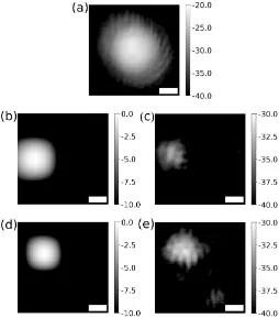
The results are displayed in figure 5. In figure 5(a), we show the image from a simple polarization rotation mirror to find the size and quality of the collimated beam. In figure 5(b-e), we show our deflected and focussed holographic image in simulation and experiment, which are in good agreement. The small differences are due to coupling between meta-atoms, fabrication errors (e.g. variation and scratches in the PMMA spacer), and residual interference from stray reflections from the experimental setup.
Major recent advances in high frequency electronics, and receiver and transmit system integration have now reached a price-point where it is commercially viable to exploit a large part of this spectrum for consumer applications, such as the increased information transfer envisaged for next gen-eration mobile telephone communications46, or the new capa-bility provided by single-chip radar for imaging or diagnostic systems, e.g. for security systems, gesture recognition, ma-terials identification, car radar, robotic applications and au-tonomous vehicles47,48. A key challenge for the realization of this roadmap is the development of low cost, low weight, re-flect, or transmit antennas that can be scaled to large areas to provide directional, high quality beams. One of the eventual goals of this work is the development of large flexible holo-graphic films at mm-wave frequencies that would offer the ad-vantage of easy retrofitting to existing design structures whilst providing a specific tailored scattering or focussing response to an incoming beam. For example, coating walls, ceilings, windows or large flat panels with such antennas has scope to significantly improve the reliability of information transfer between high bandwidth mm-wave mobile devices and local base-stations in large rooms or halls, where beam blockage at high mm-wave frequencies is expected to be a major issue. There is also scope to provide planar high gain antennas for line of sight communication links, as well as smaller systems targeting specific radar applications.
In conclusion, we have created a platform for HMSs at a wavelength of λ =3.19 mm with both rigid and flexible implementations. This flexible implementation could be ex-ploited for smart HMS patches to enhance and extend existing millimeter wavelength equipment for applications in electro-magnetic shielding and antennas. The research data support-ing this publication can be accessed athttps://doi.org/ 10.17630/162a371-10c7-4512-b678-558951c76e55.
FIG. 5. (a) Displays the experimental image given by a polarization rotation mirror, in this case from linearly polarized alongxto linearly polarized alongy. This represents the reference beam with rotated linear polarization. (b) Simulated and (c) experimental holographic images for the rigid HMS implementation deflected to one side. (d) Simulated and (e) experimental holographic images for the flexible HMS implementation deflected to a corner. All units for simulated images are on a normalized linear scale. All units for experimental images are in dBm. The scale bar is the same for each image and represents 20 mm.
This work was supported by DSTL (DASA grant ACC6004053). J.B. and J.M. contributed equally to this work. J.B. and A.D.F. acknowledge support from EPSRC (Grant Nos. EP/M508214/1 and EP/L017008/1). A.D.F is sup-ported by the European Research Council (ERC) under the European Union Horizon 2020 research and innovation pro-gramme (grant agreement No. 819346).
1G. Zheng, H. Mühlenbernd, M. Kenney, G. Li, T. Zentgraf, and S. Zhang,
“Metasurface holograms reaching 80% efficiency,” Nature Nanotechnology 10, 308–312 (2015).
2Z. Wei, Y. Cao, X. Su, Z. Gong, Y. Long, and H. Li, “Highly efficient beam steering with a transparent metasurface,” Optics Express21, 10739–10745 (2013).
3A. Arbabi, Y. Horie, A. Ball, M. Bagheri, and A. Faraon,
“Subwavelength-thick lenses with high numerical apertures and large efficiency based on high-contrast transmitarrays,” Nature Communications6, 7069 (2015). 4N. Yu and F. Capasso, “Flat optics with designer metasurfaces,” Nature
Materials13, 139–150 (2014).
5M. Khorasaninejad, W. T. Chen, R. C. Devlin, J. Oh, A. Y. Zhu, and F.
[image:4.612.316.570.52.341.2]con-length,” Scientific Reports6, 38440 (2016).
7D. Wen, F. Yue, G. Li, G. Zheng, K. Chan, S. Chen, M. Chen, K. F. Li,
P. W. H. Wong, K. W. Cheah, E. Y. B. Pun, S. Zhang, and X. Chen, “He-licity multiplexed broadband metasurface holograms,” Nature Communica-tions6, 8241 (2015).
8Y. Montelongo, J. Tenorio-Pearl, W. Milne, and T. Wilkinson, “Polarization switchable diffraction based on subwavelength plasmonic nanoantennas,” Nano Letters14, 294–298 (2013).
9H.-S. Ee and R. Agarwal, “Tunable metasurface and flat optical zoom lens
on a stretchable substrate,” Nano Letters16, 2818–2823 (2016).
10S. C. Malek, H.-S. Ee, and R. Agarwal, “Strain multiplexed metasurface holograms on a stretchable substrate,” Nano Letters17, 3641–3645 (2017). 11J. Burch, D. Wen, C. Xianzhong, and A. Di Falco, “Conformable
holo-graphic metasurfaces,” Scientific Reports7, 4520 (2017).
12L. Huang, H. Mühlenbernd, X. Li, X. Song, B. Bai, Y. Wang, and T. Zent-graf, “Broadband hybrid holographic multiplexing with geometric metasur-faces,” Advanced Materials27, 6444–6449 (2015).
13W. Ye, F. Zeuner, X. Li, B. Reineke, S. He, C.-W. Qiu, J. Liu, Y. Wang,
S. Zhang, and T. Zentgraf, “Spin and wavelength multiplexed nonlinear metasurface holography,” Nature Communications7, 11930 (2016). 14S. M. Kamali, E. Arbabi, A. Arbabi, Y. Horie, M. Faraji-Dana, and
A. Faraon, “Angle-multiplexed metasurfaces: encoding independent wave-fronts in a single metasurface under different illumination angles,” Phys Rev X7, 041056 (2017).
15D. Wen, S. Chen, F. Yue, K. Chan, M. Chen, M. Ardron, K. F. Li, P. W. H. Wong, K. W. Cheah, E. Y. B. Pun, G. Li, S. Zhang, and X. Chen, “Metasur-face device with helicity-dependent functionality,” Advanced Optical Ma-terials4, 321–327 (2016).
16L. Huang, X. Chen, H. Mühlenbernd, H. Zhang, S. Chen, B. Bai, Q. Tan,
G. Jin, K.-W. Cheah, C.-W. Qiu, J. Li, T. Zentgraf, and S. Zhang, “Three-dimensional optical holography using a plasmonic metasurface,” Nature Communications4, 2808 (2013).
17S. Larouche, Y.-J. Tsai, T. Tyler, N. M. Jokerst, and D. R. Smith, “Infrared
metamaterial phase holograms,” Nature materials11, 450 (2012). 18Y.-W. Huang, W. T. Chen, W.-Y. Tsai, P. C. Wu, C.-M. Wang, G. Sun, and
D. P. Tsai, “Aluminum plasmonic multicolor meta-hologram,” Nano Letters 15, 3122–3127 (2015).
19Y. Deng, X. Wang, Z. Gong, K. Dong, S. Lou, N. Pégard, K. B. Tom,
F. Yang, Z. You, L. Waller,et al., “All-silicon broadband ultraviolet meta-surfaces,” Advanced Materials30, 1802632 (2018).
20J. Wang, J. Ma, Z. Shu, Z.-D. Hu, and X. Wu, “Terahertz metalens for mul-tifocusing bidirectional arrangement in different dimensions,” IEEE Pho-tonics Journal11, 1–11 (2019).
21Q. Yang, J. Gu, D. Wang, X. Zhang, Z. Tian, C. Ouyang, R. Singh, J. Han,
and W. Zhang, “Efficient flat metasurface lens for terahertz imaging,” Opt. Express22, 25931–25939 (2014).
22Q. Wang, X. Zhang, Y. Xu, Z. Tian, J. Gu, W. Yue, S. Zhang, J. Han, and W. Zhang, “A broadband metasurface-based terahertz flat-lens array,” Advanced Optical Materials3, 779–785 (2015).
23R. Singh, W. Cao, I. Al-Naib, L. Cong, W. Withayachumnankul, and
W. Zhang, “Ultrasensitive terahertz sensing with high-q fano resonances in metasurfaces,” Applied Physics Letters105, 171101 (2014).
24L. Cong, S. Tan, R. Yahiaoui, F. Yan, W. Zhang, and R. Singh,
“Experi-mental demonstration of ultrasensitive sensing with terahertz metamaterial absorbers: A comparison with the metasurfaces,” Applied Physics Letters 106, 031107 (2015).
25Y. Fan, N.-H. Shen, T. Koschny, and C. M. Soukoulis, “Tunable terahertz meta-surface with graphene cut-wires,” Acs Photonics2, 151–156 (2015). 26D. Wang, L. Zhang, Y. Gu, M. Mehmood, Y. Gong, A. Srivastava, L. Jian,
T. Venkatesan, C.-W. Qiu, and M. Hong, “Switchable ultrathin quarter-wave plate in terahertz using active phase-change metasurface,” Scientific reports5, 15020 (2015).
figurable antenna using metasurface,” IEEE transactions on antennas and propagation62, 2891–2898 (2014).
28H. Zhu, X. Liu, S. Cheung, and T. Yuk, “Frequency-reconfigurable antenna
using metasurface,” IEEE Transactions on Antennas and Propagation62, 80–85 (2014).
29H. L. Zhu, S. W. Cheung, and T. I. Yuk, “Mechanically pattern
reconfig-urable antenna using metasurface,” IET Microwaves, Antennas & Propaga-tion9, 1331–1336 (2015).
30P.-Y. Chen, J. Soric, Y. R. Padooru, H. M. Bernety, A. B. Yakovlev, and
A. Alù, “Nanostructured graphene metasurface for tunable terahertz cloak-ing,” New Journal of Physics15, 123029 (2013).
31Y.-C. Song, J. Ding, C.-J. Guo, Y.-H. Ren, and J.-K. Zhang, “Ultra-broadband backscatter radar cross section reduction based on polarization-insensitive metasurface,” IEEE Antennas and Wireless Propagation Letters 15, 329–331 (2016).
32B. Orazbayev, N. Mohammadi Estakhri, A. Alù, and M. Beruete, “Ex-perimental demonstration of metasurface-based ultrathin carpet cloaks for millimeter waves,” Advanced Optical Materials5, 1600606 (2017). 33L. Liu, X. Zhang, M. Kenney, X. Su, N. Xu, C. Ouyang, Y. Shi, J. Han,
W. Zhang, and S. Zhang, “Broadband metasurfaces with simultaneous con-trol of phase and amplitude,” Advanced Materials26, 5031–5036 (2014). 34C. Pfeiffer and A. Grbic, “Millimeter-wave transmitarrays for wavefront
and polarization control,” IEEE Transactions on Microwave Theory and Techniques61, 4407–4417 (2013).
35X. Liu, K. Fan, I. V. Shadrivov, and W. J. Padilla, “Experimental realization of a terahertz all-dielectric metasurface absorber,” Optics express25, 191– 201 (2017).
36H. Zhu, S. Cheung, K. L. Chung, and T. I. Yuk, “Linear-to-circular
polar-ization conversion using metasurface,” IEEE Transactions on Antennas and Propagation61, 4615–4623 (2013).
37N. W. Caira and D. R. Smith, “Multispectral metasurface hologram at mil-limeter wavelengths,” Applied optics57, A19–A25 (2018).
38Z. H. Jiang, L. Kang, W. Hong, and D. H. Werner, “Highly efficient
broadband multiplexed millimeter-wave vortices from metasurface-enabled transmit-arrays of subwavelength thickness,” Physical Review Applied9, 064009 (2018).
39R. Gerchberg, “A practical algorithm for the determination of phase from image and diffraction plane pictures,” Optik35, 237 (1972).
40J. Goodman,Introduction to Fourier optics(McGraw-hill, 2008). 41J. A. Veerman, J. J. Rusch, and H. P. Urbach, “Calculation of the rayleigh–
sommerfeld diffraction integral by exact integration of the fast oscillating factor,” JOSA A22, 636–646 (2005).
42J. Burch and A. Di Falco, “Surface topology specific metasurface
holo-grams,” ACS Photonics5, 1762–1766 (2018).
43J. Burch and A. Di Falco, “Holography using curved metasurfaces,” in
Pho-tonics, Vol. 6 (Multidisciplinary Digital Publishing Institute, 2019) pp. 1–8. 44N. Kooy, K. Mohamed, L. T. Pin, and O. S. Guan, “A review of roll-to-roll
nanoimprint lithography,” Nanoscale research letters9, 320 (2014). 45S. M. Kamali, A. Arbabi, E. Arbabi, Y. Horie, and A. Faraon, “Decoupling
optical function and geometrical form using conformal flexible dielectric metasurfaces,” Nature communications7, 11618 (2016).
46T. S. Rappaport, S. Sun, R. Mayzus, H. Zhao, Y. Azar, K. Wang, G. N. Wong, J. K. Schulz, M. Samimi, and F. Gutierrez, “Millimeter wave mobile communications for 5g cellular: It will work!” IEEE access1, 335–349 (2013).
47J. du Preez and S. Sinha, “Practical applications of millimeter-wave an-tennas,” inMillimeter-Wave Antennas: Configurations and Applications (Springer, 2016) pp. 133–155.
48S. Dhillon, M. Vitiello, E. Linfield, A. Davies, M. C. Hoffmann, J. Booske,