Abstract--This paper presents the initial investigations in selecting the topology of the power electronic interface for an energy storage system for power levelling applications based on a novel storage device, the supercapattery. The particularities of the supercapattery device are summarized leading to a multistage power converter structure. A review of the two stage DC/DC converter structure to interface with the supercapattery and of various DC/AC inverters and conversion techniques suitable for connection to a medium voltage and high power AC grid, is given. Simulation results prove the capability of the power electronic interface to control independently and fast the active and reactive power flow which are vital in power peak leveling and power grid stabilization.
Index Terms-- Active filters, AC-DC power conversion,
Battery chargers, Battery storage plants, Capacitive energy storage, Carbon, DC-AC power conversion, DC-DC power conversion, Electrochemical devices, Energy storage, Nanotechnology, Power conversion, Power electronics, Pulse width modulated inverters, Power system dynamic stability, Reactive power control
I. INTRODUCTION
N the last 200 years, fossil fuels powered primarily the world economy mainly because they are cheap as there is no other cost associated with their production, but only with their extraction and transportation. However, as the rate of discovering new reserves of fossil fuels is exceeded by the rate they are consumed, the price increases making the use of alternative renewable energy supplies more competitive, with wind and solar energy directly converted into electricity becoming economically feasible. This is demonstrated by the rate of which the installed power in renewable capacities increased in the last 10 years. In order to increase the utilization of renewable energy sources through technologies based on photovoltaics (PVs) and fuel cells (FC), more research is needed to constantly decrease their specific costs ($/kW installed) and also to solve the biggest problem of employing renewable energy sources to power loads in a reliable way: their poor availability dependent on weather,
This work is based on a project which was funded by E.ON AG as part of the E.ON International Research Initiative (2007–Energy Storage). Responsibility for the content of this publication lies with the authors.
C. Klumpner and G. Asher are with the Department of Electrical and Electronic Engineering, Faculty of Engineering, University of Nottingham, NG7 2RD, UK (e-mail: [email protected]).
G. Z Chen is with the Department of Chemical and Environmental Engineering, Faculty of Engineering, University of Nottingham, NG7 2RD, UK (e-mail: [email protected]).
which not always matches the consumer requirements, with the obvious solution being the installation of energy storage capabilities, which again will impact the overall cost and efficiency of the system choosing the proper storage solution having the potential to ensure the success of the renewable energy alternative or push it towards failure. This makes the energy storage the weakest link in the chain, requiring the increase of the research efforts.
There are a few energy storage technologies available, each having their own advantages and drawbacks:
- electrochemical energy storage: batteries, supercapacitors, hydrogen regenerative fuel cell etc
- mechanical batteries: flywheels: high power density at high speeds, easy and cheap electromechanical conversion; however, it cannot store energy for more than a few hours (high mechanical losses due to the high speed – tens thousands RPM necessary to achieve convenient power density) and is seen as unsafe (has the potential to cause extensive damage in case of failure of the rotating mechanism at high speed);
- hydraulic/pneumatic, simple to build, but low roundtrip efficiency (especially pneumatic ones due to loss in heat during gas compression/decompression;
- reversible hydro pumping stations, basic example of the previous category for high power, achievable by equipping large hydroelectric power plants with bidirectional (bulb type) turbines;
- superconducting magnetic storage, prototypes demonstrated, however, the technology relies heavily on the superconductor technology which after more than 30 years of development, has not reached maturity;
- electrostatic capacitive storage
The technology to be used in large scale electrical energy storage facilities has to fully comply with the following requirements:
- to provide high roundtrip efficiency (higher than 80% can be considered reasonable)
- to allow fast charge/discharge (minutes-tens of minutes)
- to employ materials that are not toxic (i.e. some electrodes or electrolytes used in batteries or fuel cells may use Pb, Cd, Hg or acids), or in case of malfunction, the equipment shouldn’t be dangerous (i.e. explosion in case of batteries or disintegration in case of flywheels)
- to require little/cheap maintenance work
- to avoid the utilisation of materials with high market value (Au, Pt, Ag) or which encapsulate a high amount
Selecting the Power Electronic Interface for a
Supercapattery Based Energy Storage System
Christian Klumpner,
Senior Member, IEEE
, Greg Asher
Fellow, IEEE
, George Z. Chen
of energy when manufactured;
- high energy density to maintain plant size and real estates related cost low.
Except for the hydro pumping stations which are currently a technically feasible solution already applied and the regenerative fuel cells, which has been investigated in research, all the above mentioned systems have been designed for relatively small scale operations, such on board of hybrid/electric vehicles and/or rely on technologies not matured yet (superconductors). However, large scale energy storage, particularly for the purposes of load leveling in electricity supply, still remains a challenge.
II. THE SUPERCAPATTERY TECHNOLOGY
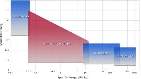
Fig. 1 shows the specific power (how fast the energy can be stored/released) versus specific energy storage capability of various electric based energy storage components.
Electrolytic capacitors are known to offer very fast charge/discharge (milliseconds) but the amount of energy they can store is still very low compared to standard lead batteries, which need very long charging times (5-10 hours). More advanced batteries such as Li-Ion, used largely on laptops, offer the best performance, with high energy densities and charging times down to one hour; however, the number of charging/discharging cycles would be affected. Fuel cells are devices that achieve a very high energy density because the electric energy is converted into chemical components which are physically separated, removed and separately, but the technology has serious limitations in terms of life cycles and cost. Supercapacitors are devices that appear on the market quite recently, and can bridge the gap between capacitors and batteries. The devices currently available on the market are optimised mostly towards offering the increased power capability in the seconds time range, whilst the minutes/tens minutes range, which is relevant to power levelling applications, remains still not covered with a proper device.
At the University of Nottingham, past research in the in the Electrochemical Technologies Group led by Prof. George Z. Chen under the support of the Engineering and Physical Science Research Council grant no. GR/R68078/01-02 has led to the invention of novel composites of redox active materials and carbon nanotubes. These are known as the third
generation energy storage materials. The unit cell made from these nano-composite materials may have a voltage of 1.0-3.0 V, mainly depending on the nature of electrolyte used. The specific capacitance of these materials ranges from 100 to 500 F/g [1]–[3]. Considering that 1.5 V is a technically viable unit cell voltage, it may be calculated that the specific energy (or energy density vs. active material mass) can reach 28-140 kJ/kg (or 8-39 Wh/kg) (vs. both electrodes in a unit cell. For each electrode the energy density would be four times higher). Preliminary results of a 9 cell supercapattery stack demonstrator reported in [4], are illustrated in Fig. 2. The electrode specific capacitance of these materials has reached beyond 5 F/cm2 (vs. surface area of electrode substrate) in laboratory tests and a cycle life beyond 5000 (1000 cycles are equivalent to 1 year for 3 charge/discharge cycles per day). With a conservation of 50% in scale up effect, a unit cell with 1 m2 electrode surface area would give rise to a cell capacitance of (50%*5*10000/2 =) 12500 F. The energy storage per cell comes to (12500*1.52/2 =) 14 kJ/cell (or ~4 Wh/cell). Because the cell can be charged/discharged in tens-hundreds sec, the power output could be far higher than what is needed for load levelling for electricity supply.
[image:2.612.53.301.260.400.2]The above estimation demonstrates the capability of supercapacitors in high power electricity management. However, it also brings about an important technical mismatch between capability of supercapacitors and the need of load levelling for urban electricity supply: the former is too fast to be utilised efficiently for the latter (minute vs. hour). It is well known that all supercapacitors exhibit a higher capacitance at a slower dis-/charging rate, mainly because of the electrode kinetics. On the other hand, at slower rates, utilisation of the active materials on the electrodes can be more complete, which in turn provides the opportunity to increase the load of Fig. 1. Specific power vs. specific energy of various energy storage
[image:2.612.324.560.450.735.2]devices.
Fig. 2. Preliminary charging-discharging results from a 9 cell
supercapattery stack [4]: a) V-I and b) V-time curves.
(a)
(b)
Voltage (V)
Equivalent Cap (F)
Equivalent Cap (F)
V
o
lt
a
g
e
(
V
)
eq
the active materials and hence the capacitance (or energy storage capacity). This gain in capacitance is of course a result of compromising the dis-/charging rate and makes the supercapacitor to perform in a manner closer to but still significantly faster than a battery. We call this battery-like supercapacitor a supercapattery, to reflect its relatively slower dis-/charging rate but higher energy storage capacity, which will be ideal for load levelling system in urban electricity supply.
III. THE POWER ELECTRONIC INTERFACE
There are clear indications [1]-[4] that the supercapattery will offer clear improvement over the other well known energy storage solutions, the capacitor-battery hybrid behaviour of the supercapattery device being able to capitalize on the advantages of both while cancelling most of their drawbacks. However, they cannot connect directly to the AC power grid; therefore. a power converter able to convert the DC to AC whilst maintaining a sinusoidal AC current in the grid and to accurately control the active and reactive power transfer used both for smoothly charging/discharging the storage device, as well as to maintain the stability of the power grid, a power electronic converter interface is needed. The role of the power electronic interface which is typically the most expensive part of the system, will be rather complex [5]-[11]:
- on the grid side: operation with distorted/unbalanced supply voltage, islanding detection, harmonic filtering, supporting the power grid with active and reactive power during a power blackout/brownout etc;
- on the energy storage side, maintaining a correct voltage balance within the series connected capacitor/battery cells in order to preserve their lifetime and to increase the utilization factor (control of cell voltage reduces the voltage safety margin increasing the cell energy output).
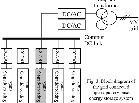
The structure of the power electronic interface is presented in Fig. 3. It consists of multiple supercapattery stacks individually connected to a common DC-bus via individual bidirectional DC/DC converters operating at high switching frequency which have the role of providing galvanic isolation of the stacks and also the possibility to individually control the power flow from the stacks depending on their state of
charge/health; in case of failure within the stack, offering the possibility of fully disconnecting the stack and removal of the faulty stack from the assembly for maintenance/repairing. Depending on the capability of the supercapattery device to withstand switching ripple stress whilst minimizing the filters size, a voltage/current mode DC/DC converter can be used.
A. The Supercapattery stack conversion stage
[image:3.612.325.551.353.439.2]Most of today’s energy storage systems (i.e. UPS) rely heavily on electrochemical battery technology, being characterized by long charging and discharging times, but by a quite narrow voltage variation range that correspond to fully discharged to fully charged state. Capacitors on the other hand, can charge and discharge much faster, however, they exchange energy by varying the voltage in a much wider range and following a quadratic interdependence with the voltage variation (i.e. during a 60% voltage drop, a capacitor releases 84% of its total stored energy) as suggested in Fig. 4. Since the supercapattery will behave as a capacitor from the point of view of how it releases the energy, it is clear that this will impose the necessity to re-evaluate the DC/DC converter that will interface with the supercapattery in order to provide best performance and lowest cost whilst the input voltage varies in a wide range (i.e. 40-100% of the rated voltage in order to utilize 84% of the total supercapattery energy).
Fig. 4. Typical voltage vs. state of charge dependence for batteries/capacitors. Since it is essential for the DC/DC converter to operate with in a wide input voltage range in order to maximize the energy exchanged with the supercapattery, additional restrictions will be imposed in order to maximize the efficiency and the utilization of components and provide galvanic isolation between the supercapattery and the DC-link of the grid side inverter. It needs to be noted that due to the particularity of the power leveling application, if is very likely that the supercapattery devices will be (dis)charged in a constant power mode. This leads to a two stage conversion (Fig. 5) that consist of a buck-boost non-isolated DC/DC converter to provide independent control (charge/discharge) of each supercapattery strack and constant output voltage (and voltage transfer ratio) facilitating an optimal design of the second DC/DC converter that includes the more demanding and expensive high frequency transformer. The presence of multiple paralleled bidirectional boost converters can in addition provide interface to mixed technology energy storage devices (ie. fast charging supercapatteries mixed with standard slow and full cycle operated charge/discharge batteries).
Since the voltage varies in a wider range than for a battery, this means that the (dis)charge currents will tend to be much higher if trying to operate the supercapattery device in the low
S u p er ca p p at te ry st ac k S u p er ca p p at te ry st ac k S u p er ca p p at te ry st ac k S u p er ca p p at te ry st ac k D C /D C D C /D C D C /D C D C /D C DC/AC DC/AC S u p er ca p p at te ry st ac k D C /D C Common DC-link Step-up transformer MV grid
Fig. 3. Block diagram of the grid connected supercapattery based energy storage system
E 100%
50% 100%
40%
84%
CAP BAT
[image:3.612.59.286.572.740.2]state of charge region, impacting directly the current rating of the semiconductor and magnetic components and indirectly the efficiency, cost and physical size of the DC/DC converter.
Fig. 5. Supercapattery bank built on a two-stage DC/DC inverter topology. B. The power grid side conversion stage
Depending on the power rating, the DC/AC inversion stage that connects towards the power grid may consist of a low voltage (<1000Vrms) or medium voltage (1-6kVrms) voltage or
current source inverter stages implemented as a single or multiple modules paralleled, so that can be operated in interleaved mode [8] in order to obtain switching ripple minimisation with reduced amount of filtering.
Using a medium voltage DC/AC inversion stage may seem the simplest choice, enabling galvanic connection to the medium voltage power bus, cancelling the need and the cost for a high power transformer. However, even though important progress has been made in the medium voltage (>6kV) forced commutated semiconductor switch technology, this devices remain quite expensive, the specific switching losses is still higher that for low voltage switches which means that the switching frequency and therefore the harmonic performance is limited. In order to improve this, interleaved operation of paralleled medium voltage DC-AC inverters, as depicted in Fig. 6 may be necessary.
Fig. 6. Topology of a galvanically connected DC/AC grid interface consisting of two paralleled voltage source inverters.
In case the converter has to be connected to a much higher voltage level power bus, which cannot be handled by current semiconductor topologies (i.e. 25 or 33kV), a step down transformer may be necessary anyway. In such a situation, a combination of a solid state forced commutated tap changer consisting of two low voltage bidirectional switches providing continuous adjustment of the output voltage [9] and a DC/AC inverter may be a possible solution (Fig. 7). Since the AC chopper uses switches rated at much smaller voltage than the
[image:4.612.316.562.134.300.2]main inverter bridge (i.e. 10%), it can switch much faster and can correct easily the supply voltage distortion and even a small degree of unbalance (2-5%), easing the DC/AC inverter stage task to achieve fast power flow control and accurate synthesis of sinusoidal line currents, which is difficult when operating with reduced switching frequency in the presence of voltage supply harmonics/unbalance.
Fig. 7. Topology of a grid interface consisting of a forced commutated AC chopper coupled to a DC/AC voltage source inverters.
However, there are great expectations from novel semiconductor materials such as SiC which may enable the appearance of superior switches commercially available in the mid term future (5-10 years) [10].
Multilevel power converter topologies relying on low voltage semiconductor switches are another alternative. Fig. 8 depicts a topology consisting of series connected H-bridges. Since the output voltage can be changed in smaller steps, it can offer an improved harmonic performance. The DC voltages can be further optimized in order to achieve best harmonic performance with minimum number of cells. Also, the use of energy storage devices in some of the cells DC-links have been reported [11]. However, the complexity of the control increases since each DC-link voltage needs to be monitored; also, the modulation becomes more complex, having to consider besides the harmonic performance, the balancing/sharing between cells of the power processed.
[image:4.612.77.273.445.613.2] [image:4.612.332.542.535.714.2]On the other hand, low voltage DC/AC inverters are currently a mature and well established technology. In addition, working with smaller voltage levels require the use of a transformer which provides additional galvanic isolation which enables the minimization of the cost with the supercapattery side conversion stage since the large number of DC/DC converters that are used, have to withstand a lower breakdown voltage. In order to achieve connection to a medium voltage system, a step down transformer is needed. Since the current handling capability of the forced commutated devices (IGBTs) is limited, multiple low voltage inverter modules may have to be used anyway and since the magnetic circuit is sized to process the full installed power, having multiple sets of isolated secondary windings may not be too expensive but can provide an important advantage: the limitation of the circulating current caused by the interleaved operation of the paralleled modules as depicted in Fig. 9.
Fig. 9. Topology of a grid interface consisting of two interleaved DC/AC inverters coupled via isolated secondary windings.
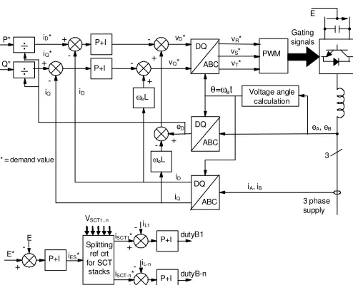
C. The control structure
A typical control structure of a back-to-back system would normally require the load side inverters to fulfil the load demands leaving the power grid stage control with the task of balancing the power drawn from the grid with the one consumed by the load. A feed-forward of the DC-link current drawn by the load inverter or monitoring the DC-link voltage deviation from the reference value (or both) can be used to find the reference active current of the grid side converter.
In this application, however it is envisaged that multiple low power rated and therefore very fast DC/DC inverters would be used to connect the supercapattery banks to the main DC-link whilst the grid power interface may consist of a single/fewer larger power rated units which would typically react much slower. In addition, since the main focus of this application is to enhance the power grid performance during faults and transients, it is chosen to build the control strategy to primarily accomplish the grid side requirements, leaving the much faster DC/DC converters and the supercapattery banks with the single task of balancing the power flow in order to maintain the main the DC-link voltage of the DC/AC inverter stage, constant. Fig. 10 shows the resulting control structure.
IV. SIMULATION RESULTS
In order to prove that a power electronic interface can fulfil the basic requirements of the energy storage system, a simulation model of two interleaved voltage source inverters connected to the grid via step down transformers, as depicted in Fig. 9, has been implemented in PSIM. The parameters of the circuit are given in Appendix A.
[image:5.612.55.298.254.423.2]Fig. 11a and 11b shows the line currents for each of the two grid connected inverters. The switching ripple is large, mainly due to the large DC-link voltage switched and the low switching frequency which is typical for high power hard-switched PWM inverters. Interleaving operation of the two inverters paralleled in the DC side which would typically cause large high frequency circulating currents, is possible without the need for common mode inductors, since the two sets of secondary windings are isolated. The benefit of interleaved operation is clearly visible in Fig. 11c, where the primary side grid currents are shown, virtually ripple free and sinusoidal.
Fig. 11. a-b) Boost inductance currents in the two interleaved DC/AC inverter units and c) the cumulated grid side currents.
(a)
(b)
(c) 3
3 phase supply ABC
DQ ABC DQ
ABC DQ
Voltage angle calculation P*
ωeL
iQ*
P+I P+I
÷
ωeL
θ=ωet
eA, eB
eD
iA, iB
iQ iD
iD* vD*
vQ*
PWM Gating signals vR*
vS*
vT*
iD
iQ
-
+
+ +
+
* ≡ demand value
+
-
- -
-
E
E* P+I
+ - ÷
Q*
E
iES*
Splitting ref crt for SCT
stacks
VSCT1..n
iL1
iSCT1* P+I
+ -
dutyB1
iL-n
iSCT-n*
P+I
+ -
dutyB-n
Fig. 10. Control structure of the supercapattery energy storage system: grid DC/AC inverter (top); supercapattery stacks (bottom) I(Lina) I(Lboost_a)
I(Lboost2a)
[image:5.612.314.564.513.716.2]Details of the switching ripple cancelation process achieved by delaying the second unit PWM generation sequence by a half switching period are revealed in Fig. 12, that shows a zoom of two currents that correspond to the same input phase.
Fig. 12. The phase A current in the two corresponding boost inductances revealing how the switching current ripple works.
Fig. 13 illustrates the grid side behaviour of the power converter assembly shown in Fig. 9 during an active power flow reversal (550Apk) that starts at t=0.175s (current and
voltage are in antiphase) and ends at t=0.25s (current and voltage are in phase). At t=0.325s, the reactive current reference is ramped up from zero (denoted by the fact that voltage and currents cross zero simultaneously) to 300Apk
(t=0.35s) which is denoted by the fact that the current starts to lead the voltage.
Fig. 13 a) Phase A grid voltage and current and b) the grid currents during a full active power reversal (tstart = 0.175; tend = 0.25s) and a reactive power
injection ramp-up from IQ = 0A (t<0.325s) to 300A capacitive (t>0.35s).
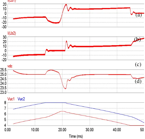
Fig. 14 shows the behaviour of a supercapattery bank that consists of two supercapatery stacks and their associated DC-DC boost converters, during a load current reversal step (t=20ms). The assumptions are that the stacks have different initial state of charge and when one of them becomes fully dis-/charged, its reference current is forced to zero to make sure it always operates within specified voltage limits whilst the remaining operational supercapattery stack has to deliver the whole reference current. It can be observed that this
[image:6.612.49.300.100.201.2]strategy will ultimately reduce the difference in the state of charge between different supercapattery stacks leading to a natural balancing of the state of charge within stacks.
Fig. 14. Transient response (4.5 A current step reversal at 20 ms) of a supercapattery bank consisting of two supercapattery strack: a-b) Stack 1 and 2 current; c) Stack output DC voltage; d) strack voltages
(unequal initial state of charge).
Due to the very fast switching and control, the boost converter can maintain the output voltage of the supercapattery bank quasi constant (25V) which would enable the main DC/DC inverter with galvanic isolation (results not included) to operate within a narrow voltage transfer (duty-cycle) range, making the design cost effective and more efficient.
V. CONCLUSIONS
This paper describes the initial investigation in exploring the configuration for a power electronic interface needed to connect to the power grid, a large energy storage unit consisting of multiple supercapattery stacks, which are novel storage device based on carbon nanotubes. The basic characteristics of the novel supercapattery device such as fast charge/discharge times and the power and energy density are introduced, justifying its use in power leveling applications. The characteristics of a few grid-side power converters suitable for high power applications are discussed. Simulation results of one of the topology consisting of interleaved voltage source inverters confirms that the system is able to provide independent and fast active and reactive power injection which is essential in supporting the grid during faults or to enhance the power system stability
VI. APPENDIX A
Circuit parameters for DC/AC inverter: E=3.6kV; fsw=3 kHz;
Lin=1.75mH; N1/N2A/N2B=1; Vin-line = 2.4 kVrms.
DC/DC boost converter: CSCT1=CSCT2=0.1F; LB1=LB2= 0.1mH;
Cdc-ES=4.7mF; fsw-B=20 kHz; VSCT1-max=8V; VSCT1-min=4V.
(a)
(b)
(a)
(b)
(c)
[image:6.612.50.300.332.587.2]VII. REFERENCES
[1] Snook GA, Peng C, Fray DJ, Chen GZ, Achieving high electrode specific capacitance with materials of low mass specific capacitance: Potentiostatically grown thick micro-nanoporous PEDOT films,Electrochem.Comm.,9(2007) 83–88.
[2] Wu MQ, Snook GA, Chen GZ, Fray DJ, Redox deposition of manganese oxide on graphite for supercapacitors, Electrochem. Comm., 6 (2004) 499-504.
[3] Hughes M, Chen GZ, Shaffer MSP, Fray DJ and Windle AH, Composites of Carbon Nanotubes and Polypyrrole for Electrochemical Supercapacitors, Chem. Mater. 14 (2002) 1610-1613.
[4] K.C. Ng, S.W. Zhang, G.Z. Chen, "An asymmetrical supercapacitor based on CNTs/SnO2 and CNTs/MnO2 nanocomposites working at 1.7
V in aqueous electrolyte", PRiME 2008, Honolulu, Hawaii, Oct. 2008. [5] G.K. Andersen, C. Klumpner, S. B. Kjær, F. Blaabjerg, "A New Power
Converter for Fuel Cells with High System Efficiency", Int. Journal of Electronics, Vol.90, No.11-12,pp.737-750, Taylor & Francis, 2003. [6] S. Srianthumrong, H. Akagi, “A medium-voltage transformerless
AC/DC power conversion system consisting of a diode rectifier and a shunt hybrid filter”, IEEE Trans. on Industry Applications, Vol. 39, No. 3, pp. 874 – 882, 2003.
[7] C. Klumpner, M. Liserre, F. Blaabjerg, “Improved Control of an Active-Front-End Adjustable Speed Drive with a Small dc-link Capacitor under Real Grid Conditions”, Proc. of IEEE PESC’04, pp#10910, 2004. [8] E.P. Wiechmann, R.P. Burgos, D. Boroyevich, “Active front-end
converter input filter minimization using sequential sampling space vector modulation for multi-motor drives”, IEEE Proc. of IAS’01, vol. 3, pp. 1687-1694, 2001.
[9] P. Bauer, “New Robust Switching Commutation for a Tap Changer”, Proc. of EPE’03, paper #0899 (CD-ROM), 2003.
[10] C. M. Johnson, “Comparison of Silicon and Silicon Carbide Semiconductors for a 10 kV Switching Application”, IEEE Proc. of PESC’04, pp. 572-578, 2004.
[11] S.Azongha, L.Liu, H.Li, “Utilizing Ultracapacitor Energy Storage in Motor Drives with Cascaded Multilevel Inverters”, IEEE Proc. of IECON’08, pp. 2253-2258, 2008.
VIII. BIOGRAPHIES
Christian Klumpner (S’00, M’02, SM’08) was born in Resita, Romania, in 1972. He received the Ph.D. degree in electrical engineering from the “Politehnica” University of Timisoara, Timisoara, Romania, in 2001. From 2001–2003, he was a Research Assistant Professor at the Institute of Energy Technology, Aalborg University, Aalborg, Denmark. Since October 2003, he has been a Lecturer at the School of Electrical Engineering, University of Nottingham, Nottingham, U,K. His research is in the area of power electronics and ac drives, with special focus on direct power conversion (matrix converters). Dr. Klumpner was awarded the Isao Takahashi Power Electronics Award in 2005 at the International Power Electronics Conference organized by the IEEJ in Niigata. He is also a recipient of the 2007 IEEE Richard M. Bass Outstanding Young Power Electronics Engineer Award.
Professor Greg Asher (SM ’02, FIEEE’07) graduated in Electrical & Electronic Engineering from Bath University in 1976. He received his PhD in 1979 in Bond Graph structures and General Dynamic Systems. He was appointed lecturer in Control in the School of Electrical and Electronic Engineering at University of Nottingham in 1984 where he developed an interest in motor drive systems, particularly the control of AC machines. He was appointed Professor of Electrical Drives in 2000 and Head of the School of Electrical and Electronic Engineering in 2004. He is currently the Associate Dean for Teaching and Learning in the Engineering Faculty at the University of Nottingham. He has published over 240 research papers, has received over £5M in research contracts. He was a member of the Executive Committee of European Power Electronics (EPE) Association until 2003, Chair of the Power Electronics Technical Committee for the Industrial Electronics Society until 2008 and is an Associate Editor of the IEEE Industrial Electronics Society.