Experimental visualization of scattering at defects in electronic transport through
a single atomic junction
Yong-hui Zhang,1,2,*Peter Wahl,1,3and Klaus Kern1,4
1Max-Planck-Institut f¨ur Festk¨orperforschung, Heisenbergstrasse 1, 70569 Stuttgart, Germany 2Department of Physics, Tsinghua University, Beijing 100084, China
3SUPA, School of Physics and Astronomy, University of St. Andrews, North Haugh, St. Andrews, Fife KY16 9SS, UK
4Institut de Physique de la Mati`ere Condens´ee, Ecole Polytechnique F´ed´erale de Lausanne (EPFL), CH-1015 Lausanne, Switzerland
(Received 14 June 2012; published 10 May 2013)
For electronic transport at the nanoscale, coherent scattering at defects plays an important role. Therefore, the capability of visualizing the influence of defects on the conductivity of single atomic junctions may benefit the development of future nano-electronics. Here, we report imaging the coherent scattering from a defect with well-controlled geometry by quantum point contact microscopy recently developed by us. An∼10% modulation in transport conductance of a single atomic junction is observed, with a phase shift of nearlyπcompared to the tunneling conductance. With the well-defined scattering geometry, we performed a theoretical calculation of the conductance and found the result consistent with the experiment.
DOI:10.1103/PhysRevB.87.205417 PACS number(s): 72.10.Fk, 73.63.−b, 85.35.−p
I. INTRODUCTION
As is well known, the rapid growth of the performance and complexity of integrated circuits (IC) is realized by continuous shrinking in the size of the embedded components. Nowadays the dimension of transistors in a CPU has reached a few tens of nanometers. It would therefore be expected that coherent scattering at defects may influence the electronic transport at the nanoscale in future ICs. For mesoscopic systems, coherent scattering leads to universal fluctuations of the conductance as a fundamental characteristic of electronic transport.1 Scanning probe microscopy has shown that the flow of charge carriers can be interrupted by a tip-induced defect in a semiconductor quantum point contact (QPC) of a submicrometer dimension.2,3At the nanoscale, conductance fluctuations in contacts consisting of single atoms or molecules have been observed as a function of applied voltage both using mechanically controlled break junctions (MCBJ)4and by scan-ning tunneling microscopy (STM),5which were interpreted in terms of coherent scattering of the charge carriers at defects embedded in the electrodes. However, transport experiments through single atomic junctions with well-controlled scattering geometry of the defects are still missing. This deficiency will be remedied by the quantum point contact microscopy (QPCM)6experiment reported in this paper.
II. EXPERIMENTAL METHODS
Experiments were performed in a low-temperature STM operating at 6.7 K on a polished and oriented Ag(111) single crystal. The Ag(111) surface was prepared by cycles of Ar+ sputtering and annealing to 800 K. Single Ag adatoms were deposited onto the atomically flat Ag(111) surface by controlled tip indentation.7 QPCM was performed by approaching the STM tip on top of an Ag adatom into contact and then scanning in constant-height mode [see Fig. 1(a) and Ref. 6 for details]. Due to the interaction with the tip apex, the silver atom which forms the point contact stays in the closest hollow site.8,9 We recorded both the current as well as the differential conductance (through a lock-in
amplifier) while scanning the point contact over the surface. The lock-in amplifier was operated at a modulation frequency
f = 9.83 kHz, an amplitude of U = 5 mVrms and a time constant of 10 ms in Figs.2(d),2(e), and3(a)and an amplitude of 20 mVrmsand a time constant of 3 ms in Figs.1(b)to1(j).
QPCM enables an investigation of transport properties as a function of lateral position with atomic resolution:6 as is schematically illustrated in Fig. 1(a), a mono-atomic step edge, which can be considered as a one-dimensional defect for the substrate surface, is located at a distance x away from the atomic contact. For a noble metal (111) surface, this leads to the well known standing wave patterns due to quasiparticle interference near the step edge,10–13 and modulates the conductance [G(x)] of the atomic contact. QPCM can thus measure the conductance modulation with atomic precision in the distance between the defect and the contact.
III. EXPERIMENTAL RESULTS
(a)
(x)
G(x) tip
substrate step edge
x
(b)
0.00V
0.47mG0
0.0mG0
(c)
-0.04V
(d)
+0.07V
(e)
+0.16V
(f)
0.00V
1.05G0
0.75G0
(g)
-0.04V
(h)
+0.07V
(i)
+0.16V
(j)0 2 4 6 8 10
0.6 0.8 1.0 1.2 1.4 1.6
Po
in
t Co
ntact d
I
/d
V
(
G 0
)
x (nm)
0.0004 0.0008 0.0012 0.0016
Tu
nn
e
lin
g d
I
/d
V
(
G0
)
( )
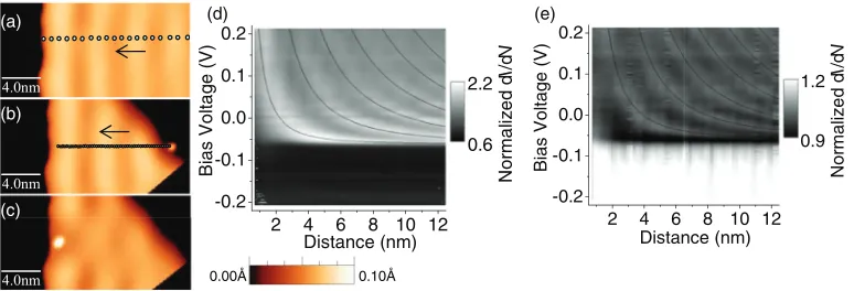
FIG. 1. (Color online) Setup and basic result. (a) Schematic illustration of conductance measurement for a single atomic junction influenced by coherent scattering from a mono-atomic step edge by QPCM. The curveρ(r) depicts the local density of states of the surface state electrons, resulting in a spatial modulation of the conductance of the atomic point contact, as is depicted by the curveG(x). Circles depict atoms. (b)–(e) Differential conductance (dI /dV) tunneling images and (f)–(i) dI /dV QPCM images acquired in constant height mode in the same area close to a step edge on Ag(111) at different bias voltages. (c)–(e) and (g)–(i) are stripes cut from the original data [see Supplemental Fig. S1 (Ref.15)] as indicated by the dotted rectangles in (b) and (f). The Ag adatom at the top center of (b) is used for performing QPCM. (j) Conductance line profiles of QPCM images (thick lines) and STM images (thin lines) along a straight line orthogonal to the step edge indicated by dashed lines in (b) and (f). Conductance line profiles taken at different bias voltages (from bottom to topU= −0.04, 0.00, 0.07, and 0.16 V), are vertically offset by 0.2G0for QPCM and 3.5× 10⁻⁴G0for STM. Conductance quantumG0=2e2/h=77.5μS.
that the conductance modulation of the atomic contact can be attributed to the oscillatory LDOS resulting from the coherent scattering by the step edge.
For both better characterization and to allow for a de-tailed comparison between the wavelength and phase of the conductance modulation found in tunneling and contact, we have measured the voltage dependent dI /dV in both regimes on the upper terrace along a line perpendicular to the step edge [see Fig. 2(a)]. For the atomic contact this implies laterally manipulating the contact atom to each position where a spectrum is recorded [Figs.2(b) and2(c)]. The tunneling spectra are shown in Fig. 2(d) and point contact spectra in Fig.2(e)as a function of bias voltage and distance from the step edge. The differential conductance at energies below the onset of the surface state relative to the energies above is significantly enhanced in point contact spectra opposite to the behavior in tunneling spectra taken on the clean surface.17,18
The interference patterns seen in Figs.2(d)and2(e) can be compared to the known dispersion of the surface state. The two-dimensional surface state has a parabolic dispersion with effective mass m∗ and onset E¯ ≡ E(k =0). Assuming a perfectly straight step edge, the contribution of the surface state to the LDOSρs including scattering at the step is11
ρs(x,E)=L0[1− |r|J0(2kx)], (1)
where L0= m
∗
π¯h2, k=
2m∗(E−E¯)
¯
h2 , r = 1 is the reflection
coefficient, x the distance from the step edge, and J0 the Bessel function of the first kind. From Eq.(1)the energyEnat which thenth maximum in the LDOS occurs at distancex is
given by
En(x)= ¯
h2
2m∗
[2π(n−1)−ϕ]2
4x2 +E¯, (2)
where ϕ is an overall phase which equals −1.25π. The differential conductance measured in tunneling is assumed to be proportional toρs. Thus by fitting Eq. (2)to the data in Fig.2(d), wherem∗ andE¯ have been adjusted such that
En(x) fits the maxima in dI /dV, we obtain an effective mass of m∗ =0.37me and an onset energy of E¯ = −0.063 eV, in good agreement with previous STS studies.19 To describe the maxima in transport spectra as shown in Fig. 2(e) by Eq.(2), also the phaseϕhas to be adjusted. The same effective massm∗ =0.37me and onset energy E¯ = −0.063 eV are obtained, however, the phase is ϕPCM = (−2.05±0.1)π, thus the phase shift between point contact and tunneling is ϕexp = ϕPCM−ϕSTM = (−0.8±0.1)π. The scattering patterns in the transport and tunneling regime exhibit within the errors the same wavelengths. We do not observe a significant Stark shift, as found for the onset of the surface state in tunneling on the clean surface,20 even though the measurement in contact is performed at conductances close to one conductance quantum.
[image:2.608.110.500.71.280.2]2 4 6 8 10 12 -0.2
-0.1 0.0 0.1 0.2
Norm
alize
d
d
I
/d
V
Bias
Volt
age
(V
)
Distance (nm) 0.9 1.2
4.0nm 4.0nm
(a)
0.00Å 0.10Å 4.0nm
(b)
(c)
2 4 6 8 10 12 -0.2
-0.1 0.0 0.1
N
o
rm
al
iz
ed
d
I
/d
V
B
ias
Vo
lta
ge (V)
Distance (nm)
0.6 2.2
(e) (d)
0.2
FIG. 2. (Color online) Differential conductance spectra in tunneling and contact as a function of position (a)–(c) STM topographies show the place where tunneling and contact spectra were acquired. (U=0.01 V,I=0.11 nA). Depression in apparent height at the right-top of (b) and (c) is due to the piezo creep. Black at the right-bottom of (b) and (c) is outside the imaging area. (d) Scanning tunneling spectra acquired at the positions approximately indicated by dots in (a), normalized differential conductance is plotted in grayscale (and smoothed) as a function of sample bias voltage and distance from step edge. (e) Point contact spectra acquired at the positions marked in (b), starting from the position of the Ag adatom in the right corner and ending at the step edge in the left. During the measurement, the Ag adatom which forms the contact follows the tip from its position in (b) to that shown in (c). Solid lines in (d) and (e) indicate the positions of local maxima of the standing wave pattern of the Ag(111) surface state according to Eq.(2)[withm∗=0.37me,E¯ = −0.063 eV, the position of the step edgex0= −3 ˚A, the phase isϕSTM= −1.25πin (d) andϕPCM= −2.05πin (e)].
it will increase the energy dissipation near the atomic contact and thus the tip tends to become unstable. As a result, the Cu(111) surface state has not been investigated to the same level as for Ag(111).
IV. COMPARISON TO THEORY
Precise knowledge of the scattering geometry enables us to compare the measured conductance fluctuations of a single atomic contact with known theory. The LDOS in STM images is calculated accounting for the interference pattern of the surface state scattered from the step edge.11 Subsequently, the effect of the quasiparticle interference patterns in the
LDOS on the transport through the atomic point contact can be modeled by an Anderson-Newns model considering two adsorbate levels between the tip and the sample representative of the surface atom and the atom at the tip apex.17,22 Both are assumed to be of the same kind with the adsorbate level at the same energy εa . Further, the level of the adatom at the surface is coupled to the surface and bulk bands of the substrate, while the level of the tip atom is coupled to the bulk bands of the tip. Between the two adsorbate levels, a coupling t is assumed. The application of the nonequilib-rium Greens function (NEGF) technique yields the transport current as22
I = 8|e| h |t|
2
εF+eV
εF
dε ImbIm[b+s(ε)]
|(ε−εa−eV−b)[ε−εa−b−s(ε)]− |t|2|2
. (3)
The contribution of the bulk states to the self-energy is assumed to be constant (b = −ib) and to be the same for the tip and surface. The LDOS of the surface state [Eq. (1) with
L0=1] enters through the self-energy of one of the leads: The imaginary part of the contribution to the self-energy from the surface state is Ims= −sρs(x,E)∗L(E;), yielding the real part from a Hilbert transform as Res=H(Ims), where
Hdenotes the Hilbert transformation, L(E;)=/[2π(E2 + 2/4)] is a Lorentzian function,∗denotes convolution, and
s is a constant. The LDOS is convoluted by the Lorentzian L(E;) to account for lifetime broadening, where is the inverse lifetime of the surface state. The contribution to the self energy from the surface isb +s. Thus the self-energy of the surface includes the scattering at the step edge through the LDOS, but scattering at the contact itself is neglected. For the parameters of the surface state, we use the effective mass
m∗and the onset energy E¯ obtained from our experimental data;r=111and=7 meV (Ref.17). For the parameters of
Eq.(3), we use the values given for a silver adatom on Ag(111) in Ref.17(εa=0.5 eV,b=0.8 eV, ands=0.5 eV). The consistency of the calculated conductance modulation with those measured in contact, which is shown below, indicates that neglecting scattering at the point contact is a reasonable assumption.
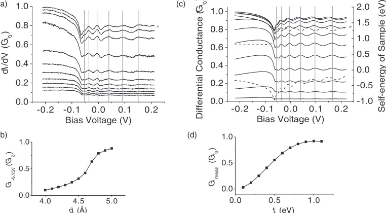
[image:3.608.112.499.72.204.2](a) (b) (c) (d) 0.0 0.2 0.4 0.6 0.8 1.0
Differential Conductance (
G 0
)
Bias Voltage (V)
-1.0 -0.5 0.0 0.5 1.0 1.5 2.0 *
Self-energy of Sample (eV)
0.0 0.5 1.0 G m ean ( G 0 )
t (eV)
0.0 0.2 0.4 0.6 0.8 1.0 d I /d V ( G 0 )
Bias Voltage (V)
*
-0.2 -0.1 0.0 0.1 0.2
0.0 0.5 1.0
-0.2 -0.1 0.0 0.1 0.2
4.0 4.5 5.0
0.0 0.5 1.0 G -0 .15V ( G0 )
[image:4.608.115.496.73.283.2]d (Å)
FIG. 3. Conductance modulation as a function of tip-sample distance. (a) Series of dI /dV spectra from tunneling to point contact. The spectra are taken by approaching the tip by different distances over the center of the Ag adatom shown in Fig. 2(b). The wiggles due to coherent scattering of quasiparticles in the surface state are clearly resolved. Vertical lines mark positions of maxima in the conductance trace for comparison. An asterisk to the right marks a spectrum acquired at similar conductance as spectra in Fig. 2(d). Panel (b) shows the conductance at −0.15 V of spectra in (a) as a function of vertical tip position d, the transition from tunneling to point contact can be clearly identified. Each point in (b) corresponds to a single spectrum in (a). (c) Calculated series of differential conductance spectra according to the model discussed in the text for an adatom at a distancex=129 ˚A from the step edge [consistent with the distance of the adatom in Fig. 2(b)]. The differential conductance (solid lines) is plotted together with the imaginary part −Im[b
+ s (E)] (upper dashed line) and the real part Re[b + s (E)] (lower dashed line) of the self-energy in Eq. (3). −Im[b +
s (E)] is proportional to the LDOS in Fig. 4(a). Vertical lines mark positions of maxima in the conductance trace for comparison. An asterisk to the right marks a spectrum calculated with the same parameters (in particular t = 0.8 eV) as in Figs. 4(a) and 4(c). (d) Mean conductance of spectra in (c) is plotted as a function of tip-adatom couplingt. Each point in (d) corresponds to a single spectrum in (c).
state is probed through the contact atom or not,21 rather than being a specific property of measuring in the transport regime. Figure 4(a) shows the calculated LDOS and transport conductance at zero bias voltage as a function of distance
x from the step edge. Except for x =0, where the atomic contact is lost at the step edge, the long-range conductance modulation from measurements as well as the contrast inver-sion between QPCM and STM images is nicely reproduced. Figures 4(b)and4(c) show the calculated LDOS and point contact spectra resembling the ones shown in Figs. 2(d)
and 2(e). By fitting Figs. 4(b) and 4(c) the phase shift
ϕcal =ϕQPCM−ϕSTM = (−0.85±0.1)π can be obtained, which is consistent with the experimental result (−0.8±0.1)π. The consistency between the experiment and theory confirms that the conductance modulation measured by QPCM is well described by the theory.
The phase shift of nearlyπbetween the LDOS and transport conductance is rather counterintuitive. To gain some physical insight, the differential conductance of the single atomic junction is explored by calculating its dependence on model
(a) 0.0 0.2 0.4 0.6 0.8 1.0 Di ff ere nt ial Cond uct an ce ( G0 )
Distance from Step Edge (nm) 0 1 2 3 L o c a l D e n s it y of S tat es ( 1 /n m /e V )
0 2 4 6 8 10 12
-0.2 -0.1 0.0 0.1 0.2 L oc al Dens it y of States ( 1 /nm /eV) Bi as V o lt a ge ( V ) Distance (nm) 0.0 2.2 (b)
0 2 4 6 8 10 12
-0.2 -0.1 0.0 0.1 0.2 Di ffere nti al Con ducta nce ( G0 ) B ias Vol ta ge (V) Distance (nm) 0.7 1.0 (c)
0 5 10 15
[image:4.608.91.520.585.689.2](a)
tip
substrate defect
x
b
t b s0
s(x)
2 1 VD 2 1
VG x
[image:5.608.78.271.70.167.2](b)
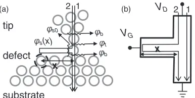
FIG. 5. Model for phase shift and QUIT. (a) Interpretation of the phase shift due to interference of two distinct paths 1 and 2 between tip and substrate. Circles depict atoms; curly lines depict phase shifts from bulk states to adsorbateϕb, between adsorbatesϕt, from surface state to adsorbateϕs0, and inside surface stateϕs(x). (b) Schematic of QUIT following Refs.25–27.
parameters (εa, b, s, and t) in Eq. (3). The calculation results (see Supplemental Figs. S2 to S4) are summarized in the Supplemental Tables S1 to S4.15 The calculated phase shiftϕcal is found to depend mainly on the energy of the adsorbate level (εa) and—through the width of the adsorbate level—on the coupling to the bulk states (b). It appears that, for resonant transport (e.g.,|εa| b),ϕcal is close toπ, while it is rather close to 0 for off-resonant transport (e.g.,
|εa| b). Therefore the calculation suggests that the phase shift close toπ is a property of resonant transport through the single atomic junction. On the other hand, off-resonant transport is expected to be relevant, e.g., for rare gas atoms23 or molecules which do not have a state at the Fermi level.24
V. PRACTICAL IMPLICATION OF THE RESULTS Our measurement can be interpreted as an interferometric determination of the phase shift associated with the trans-mission from the adsorbate level to the surface state. In the model depicted by Fig.5(a), the interference of two different paths [labeled 1 and 2 in Fig. 5(a)] between the tip and the substrate yields the total transmission. Path 2 includes going in and out of the surface state and path 1 does not, thus the phase difference between the two paths is ϕPCM =2ϕs0 +
ϕs(x), where theϕs0andϕs(x) are described in Fig.5(a). With similar considerations tunneling to the clean surface lead to a phase difference ofϕSTM=ϕs(x). Thus the measured phase difference between these two measurement geometries is 2ϕs0 and accounts for the phase shift due to transmission through the adsorbate level to the surface state. The determination of the phase shift is possible because the quantum interference patterns can be compared between the measurements in tunneling and in contact, providing a direct link between the scattering geometry and its influence on quantum transport through a single atom junction.
Furthermore, the measurement setup depicted in Fig.5(a) bears striking similarities to the proposal [Fig. 5(b)] of a quantum interference transistor (QUIT),25–27 where changes in the quantum interference occurring in a side arm to the main transport channel—in our case the surface state constitutes the side arm—are used to switch the conductance between the source and drain—in our case the tip and substrate. In the case of QUIT, the length of the side arm is controlled by a gate voltage, whereas here it can be controlled by the position of the adsorbate. It could be envisioned that in realizations with a gated two-dimensional electron gas (2DEG), the conductance could also be tuned by changing the Fermi wave vector. While in the geometry studied here changes in the conductance are only on the order of 10%, this effect is expected to be dramatically increased, e.g., in resonator structures assembled by atomic manipulation, where the modulation of the LDOS becomes stronger.14,21 Compared to QUIT devices studied previously (see, e.g., Ref. 28), by using a point contact in the geometry discussed here a reduction in size to the ultimate atomic scale becomes conceivable.
In the semiconductor industry, noble metals are widely used in the fabrication of ICs: Since 199729 copper interconnects have been used to transport charges between various electronic devices embedded in very large-scale integrated circuits, based on which CPUs in most recent desktop/laptop computers are built. Noble metals are also used as materials for electrodes and gates in the research of nanoelectronic devices. In this work, both the experiment and calculation were performed solely for noble metal surface states [Ag(111) in particular] scattered from a one-dimensional (1D) defect, but they are versatile and are in principle applicable to study the charge transport through single atomic junctions of other materials, or with complicated scattering geometry in the electrode.
As more and more transistors are integrated into the same area of a silicon die, embedded electrical devices and interconnects are becoming smaller. One would expect they eventually shrink down to the size of a few nanometers or even a few angstroms. Consequently, the knowledge of how atomic defects change the conductance of both an electrical device and interconnect may become important for the design of future ICs. In this regard, both the conductance modulation we observe and the QPCM method may find their application in the design of future ICs and nanoelectronic devices, where defects play an important role in the electronic transport at the atomic scale.
ACKNOWLEDGMENTS
P.W. acknowledges discussions with W. Belzig. Y.Z. ac-knowledges support by the Chinese Scholarship Council.
*Correspondence should be addressed to: zhangyonghui02@ tsinghua.org.cn
1Y. Imry,Introduction to Mesoscopic Physics(Oxford University Press, New York, 1997).
2M. A. Topinka, B. J. LeRoy, S. E. J. Shaw, E. J. Heller, R. M. Westervelt, K. D. Maranowski, and A. C. Gossard,Science289, 2323 (2000).
3M. A. Topinka, B. J. LeRoy, R. M. Westervelt, S. E. J. Shaw, R. Fleischmann, E. J. Heller, K. D. Maranowski, and A. C. Gossard, Nature (London)410, 183 (2001).
4B. Ludolph, M. H. Devoret, D. Esteve, C. Urbina, and J. M. van Ruitenbeek,Phys. Rev. Lett.82, 1530 (1999).
6Y. Zhang, P. Wahl, and K. Kern,Nano Lett.11, 3838 (2011). 7L. Limot, J. Kr¨oger, R. Berndt, A. Garcia-Lekue, and W. A. Hofer,
Phys. Rev. Lett.94, 126102 (2005).
8J. A. Stroscio and R. J. Celotta,Science306, 242 (2004).
9A. Sperl, J. Kr¨oger, and R. Berndt,Phys. Rev. B81, 035406 (2010). 10S. D. Kevan and R. H. Gaylord,Phys. Rev. B36, 5809 (1987). 11M. F. Crommie, C. P. Lutz, and D. M. Eigler,Nature (London)363,
524 (1993).
12Y. Hasegawa and Ph. Avouris,Phys. Rev. Lett.71, 1071 (1993). 13L. B¨urgi, O. Jeandupeux, H. Brune, and K. Kern,Phys. Rev. Lett.
82, 4516 (1999).
14M. F. Crommie, C. P. Lutz, and D. M. Eigler,Science262, 218 (1993).
15See Supplemental Material at http://link.aps.org/supplemental/ 10.1103/PhysRevB.87.205417for supplemental tables and figures. 16J. M. Krans, J. M. van Ruitenbeek, V. V. Fisun, I. K. Yanson, and
L. J. de Jongh,Nature (London)375, 767 (1995).
17L. Limot, E. Pehlke, J. Kr¨oger, and R. Berndt,Phys. Rev. Lett.94, 036805 (2005).
18F. E. Olsson, M. Persson, A. G. Borisov, J.-P. Gauyacq, J. Lagoute, and S. F¨olsch,Phys. Rev. Lett.93, 206803 (2004).
19L. B¨urgi, L. Petersen, H. Brune, and K. Kern,Surf. Sci.447, L157 (2000).
20L. Limot, T. Maroutian, P. Johansson, and R. Berndt,Phys. Rev. Lett.91, 196801 (2003).
21J. Kliewer, R. Berndt, and S. Crampin,Phys. Rev. Lett.85, 4936 (2000).
22N. N´eel, J. Kr¨oger, R. Berndt, and E. Pehlke,Phys. Rev. B78, 233402 (2008).
23A. Yazdani, D. M. Eigler, and N. D. Lang,Science272, 1921 (1996). 24A. Nitzan and M. A. Ratner,Science300, 1384 (2003).
25F. Sols, M. Macucci, U. Ravaioli, and K. Hess,Appl. Phys. Lett.
54, 350 (1989).
26S. Datta,Superlattices Microstruct.6, 83 (1989). 27F. Capasso and S. Datta,Phys. Today (2)43, 74 (1990). 28T. J. Thornton,Rep. Prog. Phys.58, 311 (1995).