TRANSISTOR AMPLIFIERS
Thesis by Aldo Gene DiLoreto
In Partial Fulfillment of the Requirements For the Degree of
Doctor of Philosophy
California Institute of Technology Pasadena, California
ACKNOWLEDG~mNTS
The author is particularly grateful to Dr. R. D. Middlebrook for his guidance and continual encouragement in the preparation and com-pletion of this work. Gratitude is also extended to Drs. H. Martel and C. Wilts for their assistance in the preparation of the final text.
Personnel of R. C. A. Laboratories, Raytheon, and Telefunken generously donated the transistors used in this investigation; Aerojet -General Corporation loaned the test equipment used in the low-frequency studies. Appreciation is expressed to them for this invaluable assist-ance.
I'lethods of minimizing the effects of internally generated noise in transistor amplifiers are described. The study is both theoretical and experimental in nature, the greater part of the theoretical portion being based on van der Ziel1s transistor noise model. From this model, analyt-ical expressions are formulated giving (in terms of easily measurable transistor parameters) the operating point and source resistance that will optimize the noise performance of the amplifier. The derived equations are substantiated by an experimental study. Both audio and radio frequency amplifiers are considered. At audio frequencies, the work is primarily experimental in nature. Here, attention is focused on developing a simpli-fied optimization procedure. For the radio frequency amplifier, formulas are also derived that describe the effect of source reactance on the ampli-fier1s noise performance.
Formulas giving the noise figures of the transformer-coupled transistor amplifier are included. From these equations, analytical expressions are formulated that describe the emitter current and transformer turns ratio which will minimize the effects of internally generated noise. An experi-mental investigation verified the results.
A portion of the work is devoted to a theoretical and experimental study of temperature and its effect on the noise performance of transistor ampli-fiers. This study, which considers temperatures from
77
to 320 K, differs o from those previously conducted in that a wide range of source resistances are used.Equations describing the degradation in noise performance produced by resistive stabilizing components are given.
TABLE OF CONTENTS
INTRODUCTION
Concept of Noise Performance Definitions of Noise Performance Optimum Noise Performance • The Optimization Problem Explicit Parameter Dependence
Effect of Source Impedance on Noise Performance Frequency Dependence of Noise Factor Parameters Brief Resume of the Remaining Controllable and
Uncontrollable Parameters Example of an Optimization Problem
The Three Frequency Regions A BRIEF DESCRIPTION OF THE THESIS
Mean Frequency Region Ilf Frequency Region High Frequency Region Transformer Coupling Temperature
Emitter Degeneration, Bias Stabilization Load Resistance and Multistaging
Measuring ~lethods 1. MEAN-FREQUENCY REGION
Mean-Frequency Noise Model
Common-Base and Common-Emitter Amplifiers Common-Collector Amplifier
Experimental Measurements
Source ReSistance as an Uncontrollable Parameter Equivalent Noise Resistance •
Collector Voltage and Its Effects on
Mean-Frequency Noise Performance Conclusions
2. l(f FREQUENCY REGION
l(f and Transition-Frequency Noise Models Simplified Optimization Procedure •
3. HIGH FREQUENCY REGION
van der Ziel1s Noise Model
Common-Base and Common Emitter Amplifier Common-Collector Transistor Amplifier Experimental Technique
Conclusions
4. TRANSFORMER COUPLING
Transformer-Coupled Common-Base and
Common-Emitter Amplifier Transformer-Coupled Common-Collector Amplifier Experimental Verification of the Derived Results
5.
TE~lPERATURE.Experimental Study
~lean-Frequency Theoretical Study Conclusions
6
.
BIAS STABILIZATION AND EMITTER DEGENERATIONEffect of Bias Stabilization on Noise Performance Emitter Degeneration
Conclusions
7.
LOAD RESISTANCE AND MULTISTAGINGof Transistor Amplifier
Effect of Load Resistance on Noise Performance Multistaging
8. MEASURING METHODS
79
80 82
89
91
96
97
97 101 101 106
106 III 119 120
120 123 125 126 126 128
131 Transistor Noise Factor !·leasurements 131
Continuous-Wave Method . 131
Noise Injection Method . 133
Effects of Equipment Noise on Noise Factor Measurements 135
Indicating Device Error 138
9.
CONCLUSIONS 1411 INTRODUCTION
In the 14 years that have elapsed since the development of the first experimental transistors, several investigations have been con -ducted in an effort to formulate models that would describe the mean -square magnitude of noise fluctuations observed at the output terminals of a semiconductor diode or transistor. Owing to the spectral character of the observed noise, universal models have not yet been forthcoming. However, van der Ziel (Ref. 1) and Guggenbuehl (Ref. 2), utilizing
results obtained by Johnson (Ref.
3)
and Schottky (Ref.4),
independently formulated equations that describe (for a limited portion of the fre -quency spectrum) the mean-square magnitude of fluctuations produced by current flow across a semiconductor diode junction. The diode equations were later extended by van der Ziel to include the effect of random diffusion and recombination-regeneration which occurs in the base region of a semiconductor triode.Van der Ziel 's triode model, while subject to restrictions not often met in design practice (and restricted to the frequency region where l/f noise can be neglected) forms a basis from which operating parameters can be found that will minimize the effects of internally generated amplifier noise.
Formulating equations that describe the source resistance and emitter current that will minimize the effect of noise in the unconstrained ampli -fier.
Formulating equations that describe the optimum emitter current in an amplifier constrained by a fixed-source resistance.
Formulating equations that describe the optimum turns ratio and emitter current in a transformer-coupled amplifier.
Formulating equations that describe the effect of source reactance on the high-frequency amplifier.
Formulating equations that describe the effect of temperature on the noise performance of the amplifier.
Formulating equations that describe the degradation in nOise perform -ance produced by resistive stabilizing components.
At low audio frequencies, the spectral density of the noise observed at the output terminals of a transistor amplifier follows a phenomenolo -gical inverse frequency dependence. This noise, called l/f or excess noise, is caused by a yet-undetermined surface phenomenon. Hence, an analytical model that accounts for the mean-square magnitude of the ob -served noise has not been formulated. However, Fonger (Ref. 5) in his investigation of excess noise proposes an empirical noise model for the transistor amplifier in which each of the noise generators contained in the model has a mean-square value, K
If
.
Each of the constants but onen
of Ilf noise in a transistor amplifier). It does become possible, however, Hith the assumption that the noise sources contained in the amplifier have
a Ilf frequency dependence, and Vlith the further assumption that the noise sources are not functions of the driving-point impedance, to obtain opti -mization parameters from a limited number of noise measurements.
Yajimi (Ref.
6
),
utilizing the results of both Fonger and van der Ziel, has developed an empirical noise model for the predominant Ilf nOise generator. From the results of an experimental investigation contained in this dissertation, it was found that Yajimi1s model can be used to obtain an optimization procedure whereby the values of emitter current and source resistance which will minimize the effect of Il f noise can be obtained from a single small-signal transistor measurement.CONCEPT OF NOISE PERFORMANCE
A linear amplifier is a device used to obtain a power-amplified linear representation of a time-varying input signal. Owing to the spectral
properties of the input waveform and the noise processes inherent in the device, it is impossible to obtain perfect fidelity from a realizable amplifier. This becomes apparent when these spectral and nOise properties are considered. Since information is contained in the input signal, a transformation from the time to the frequency domain reveals that the sig-nal is dispersed over a range of frequencies, and the amplifier must have a bandwidth including these frequencies in order to reproduce this waveform. Inherent in the active and resistive components of the device are noise voltages "lhose magnitudes are functions of the bandwidth of the amplifier. Statistical distortion, resulting from this noise, prevents a perfect
reproduction of the input waveform from appearing at the output. A
determines the maximQm sensitivity of the amplifier and also describes its noise performance.
DEFINITIONS OF NOISE PERFORr~NCE
The output signal-to-noise ratio is a function of (1) the nOise generated in the driving source impedance, and (2) the noise generated in the amplifier. North (Ref.
7)
,
recognizing the need for a figure which was a basic measure of the noise generated in the amplifier, intro-duced the concept of noise factor. Friis (Ref.
5
),
in a later paper, defines the noise factor F as the ratio of the available signal-to-noise power that is measured at the source to the amplifier to the available signal-to-noise power that is measured at the output. Or, in symbolic form,F
(
Si
N
)
as(1)
(
SI
N
)
aoIt is implicit, from Friis1s definition, that conjugate matching
is required at both the input and output terminals of an amplifier when noise factor measurements are made. Since stringent implementation of conjugate matching is impossible when wide-band measurements are attempted (due to reactive components existing at the input and output terminals of the amplifier), it becomes necessary to introduce a second definition for the noise factor. This definition removes the restriction of conjugate matching and is written
F
=
(2)5
inter-changeably in the literature. The anomaly that exists between
Friis1s definition and equation 2 can be removed if the frequencies in
-fluencing a noise factor measurement are limited by bandpass circuits to
an incremental portion of the frequency spectrum. This concept results
in a third figure for F called the spot noise factor. In equation form,
the spot noise factor is written
F =
(S/N)as
(
SIN
)
ao(S/N) s
All the measurements contained in this dissertation are spot noise measure
-ments. Unless otherwise specified, the term "noise factor" whenever used
will imply spot noise factor.
With the concept of spot noise factor defined, it now becomes possible
to obtain, in equation form, a figure which describes the noise factor of
the j,Tide-band amplifier. This becomes
F
=
(4)Vlhere F(f) is the spot noise factor and G(f) is the power gain of the
amplifier, and F is a fourth figure called the average noise factor. In
practical applications, equation 4 is solved by numerical integration.
*A proof which shows the equivalence of equations 3a and 3b is contained
Two other parameters frequently used to describe an amplifier's noise performance are the noise temperature T aa nd the equivalent noise resist -ance R
eq Equations that define these parameters can be derived if all the noise sources contained in the amplifier are grouped into one voltage generator e , placed in series with the driving source impedance. With
na
this configuration, the noise factor becomes
"'""2
e +"'""2
eF ns
"'""2
na
(5)
e ns
where e~s represents the mean-square value of noise from the driving source impedance. If a resistive source in thermal equilibrium is assumed, this quantity becomes
"'""2
e=
4kT R Bns s s (6a)
Here, k is Boltzmann's constant; T is the absolute temperature of s
the source in degrees Kelvin, and B is the noise bandwidth of the ampli -fier.
The noise bandHidth is defined by
OC)
,~
I
A(f)
1
2dfB
=
I
Ao
l2
where Ao is the mid-frequency voltage gain of the amplifier. The amplifier noise temperature is defined by
"'""2
ena 4kT a s R B and becomes, from equations
5
,
6,
and7
(6b)
7
The equivalent noise resistance of the amplifier is defined by
Ij.kT R B
s eq
and becomes, from equations
5, 6,
and 9aR
eq
(930)
(9b)
Although the noise temperature is often used to describe the noise
performance of the maser and parametric amplifier, it is seldom used as
a noise parameter for amplifiers in which the active device in the input
stage is a vacuum tube or a transistor. The equivalent noise resistance
is frequently used to specify the noise performance of the vacuum tube
amplifier. However, it is found that the noise factor lends itself more
readily to the transistor amplifier optimization problem; for this reason,
it is on this noise parameter that attention is focused here.
OPTnlUM NOISE PERFORMANCE
The noise factor as defined by equation 2 can also be written in the
form
(10)
It is apparent from equation 10 that the problem of optimizing the
noise performance of an amplifier, which entails maximizing the
signal-to-noise ratio at the output, is in fact twofold. It consists of maxi
-mizing the signal-to-noise ratio of the source, and it entails minimizing
the noise factor.
To determine when the signal-to-noise ratio of the source and the
noise factor can be optimized separately, equation 10 is differentiated.
This yields
that
dF
=
d(S/N)s=
0 (12 )However, F and (S/N)s may each be functions of several controllable and uncontrollable parameters,* e.g.,
F
¢2(P nT 'l" " 'P~' ~ ql""'o ~ )
Total differentiation of these two equations yields
d
(
~
)
s
dF + ••• + ~
of _
aq .qj :
,
Controllable Parameters
of
of
+ ~ dp. 1 + ... + ,""'S~-dp
OPi+l l+ oPn n
of
of
+ ~ dq
J'+l + ••• +
2la
d'Imqj+l 1l!
..
o
(
~
)
s =~ Pn+l
..
..
f"Uncontrollable Parameters
o
(
~
)
o
(
M
dPn+l + ••• + ~ s dPk +~ds qlPk ql
'i'"
Controllable Parameters
o
(
~
)
s+. . . + ---.;:-- d P
op r r
T
Uncontrollable Parameters
j
o
{
*
}
s+ •.• +
To-:-
dq.qj J
o
(
~
)
s+ ... + ~ d'Im qm
,
(13a)
(130)
(14a)
(14b)
9
It follows from equations 12, 14a, and 14b, since dF must be zero for independent parameter variations, that optimum noise performance requires
of
of
of
0=
e)Pi
=
(lql=
d<ij
= (15a)=
o
(
~
)
o
(
~
}
o
(
~
)
s s s
0
=
~
=
~
=
dcij
=
o
(
~
}
s
(lPn+1 (15b)
Equations 15a and 15b show that if the signal-to-noise ratio of the source and the noise factor are both functions of tne same controllable parameters, ql •.. qj' the signal-to-noise ratio of the source and the noise factor can be separately optimized only if the optimUf.1 values of ql •.. qj will both minimize F and maximize (S/N)s. One frequently encountered, mutually dependent, controllable parameter is the source resistance, R . In general, the same value of R will not simultaneously
s s
minimize F and maximize (S!N)s. However, in this case, it becomes possible to interpose a transformer between the driving source and the input to the amplifier that will satisfy the constraint imposed by equations l5a and 15b.
THE OPTHlIZATION PROBLEf.!
are as follows:
1. Operating Voltage, V 2. Operating Current, I 3. Configuration, C 4. Source Resistance, Rs
5
.
Frequency, f6
.
Temperature, TAs an implicit function of these parameters, the noise factor F may be written
F = .~;\ (V, I, C, Rs' f, and T)
and the noise factor total differential dF is then
dF
~' ________ ~y~ ____________ - JJ
Controllable Parameters
y
Uncontrollable Parameters
(16a)
(16b)
The solution to the amplifier optimization problem entails finding the circuit and operating point parameters that concurrently satisfy
OF
0 (17a )
dv
=of
0 (17b)dr
of
0 (17c)de
=o
f
0 (17d)11
EXPLICIT FARM'JETER DEPENDENCE
Each of the four differer.tials contained in equations 17a, 17b, 17c,
ar.d 17d is an implicit function of the controllable and uncontrollable
parameters V, I, C, Rs' f, and T. An explicit dependence is required for
the general solution of the optimization problem. If it is assumed the
statistical properties of the noise sources contained in an amplifier are
not functions of the driving source impedance, zs' it is possible to formu -late the noise factor of the amplifier as an explicit function of this
parameter. This dependence is obtained in the following manner.
Effect of Source Impedance on Noise Performance
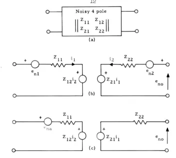
Part a of fig. 1 shows the amplifier to be analyzed. The equivalent
circuit shown in Part b of fig. 1 is obtained by utilizing the results of
Peterson1s equivalence theorem.*
From Part b of fig. 1, the output open-circuited noise voltage becomes
e2
no
=
From equation 18, the mean square noise voltage can be Hritten
(18)
(
19)
where e
nl*en2 is a measure of that cross correlation that exists between
the two noise sources.
*The equivalence theorem (Ref.
9)
states that the statistical properties().
-II
Zl1Z21
Z
1
2
11
Z22 ~
(a)
(b)
+
[image:17.536.59.411.48.364.2]( c)
Figure 1. (a) Noisy 4 Pole, (b) Two Generator Equivalent Represen
-tation of Noisy 4 Pole, (c) One Generator Equivalent.
If it is assumed the driving source is in thermal equilibrium, the
rr.ean square source noise voltage becomes
""2
ens = 4kTR e (Z s )B (20)
where R e (Z s ) sig~ifies the real part of the driving source i~pedance. Fron equations 2 and 20, the noise factor becones
F
Letting
41d'R (Z )B
e s
+ jX
s
=
Z
s
R
e
[
~
2
(
Zll
+ ZS)/Z2J 21<TR e (Z s )013
c + jC
=
Cr x
Equation 21 then reads
F
=
1 +4-kTR B
s
With the introduction of four noise factor parameters that are inde
-pendent of the source impedance, equation 22 can be simplified to read
K -'- Rno (1 + kl X + Gnc X2) + G R
o R s \ R no s R no s nc s
F
where, from equations 22 and 23, the newly defined noise factor
parameters are quantified by
2
(-
r
K 1
e
n2 rll
'
I
_e~l
cr r 2l + cxx2lJ
(23a)-'-
-0 2kTB 2 2
e~2
rllr
2l+x2l
-2 2 (e2 e2 ) 1 12
,
t
2
(rll-Lxll ) 2 nl n2 IR 4kTB e
n1 + en2 , dr(rllr21 +xllx2l)
no 2 2 2 2
(r
21-,-x2l) r 2l +x2l L.
+
c
x(rllx2l - x11r2 ,)
l
}
(23b)2
Ge
n2
(23c)
nc 2 2
4-kTB(r
= ----=1::.,,2,---;:::2- l-e
n
~
x 11 -2kTB( r 21 t-x2l )(23d)
Equation 23 describes how the noise performance of any four-terminal
nehlOrk (subject to the restrictions previously imposed) can be expected
to vary as a function of the resistive and reactive components of the
driving source impedance. A quantitative analysis that includes ::lore
fully the effect of source reactance on the optimization problem is in
-cluded in the text of the dissertation. At the present time, only that
class of optimization problem in which Xs is zero is considered.
\'iith this restriction, equation 23 simplifies to
R
F k + - -no + G R (24)
0 R nc s
s
It is found, from equation 24, that under any given set of operating
conditions a source resistance exists Hhich minimizes the noise factor of
an a~plifier. This value of source resistance, obtained by differentiating
equation 24 \>lith respect to R , becomes
s
R
so (25a)
Substitution into equation 24 gives for the rr.inimur:l noise factor
F
min k o + 2(G nc no R )1/2 (25b)
Equation 25b forms a partial solution to the optimization problem in
that it satisfies the constraint imposed by equation 17d. However, the
magnitude of the three noise factor parameters k , R , and G and hence
o no nc
the minimum noise factor are still implicit functions of the operating
15
Frequency Dependence of Noise-Factor Parameters
The statistical properties of a noisy 4 pole with unilateral or bi -lateral transmission properties can also be described using the one gener-ator noise model shown in part c of figure 1. However, now the noise voltage e shown in this figure is a function of the source impedance.
na
Since the spectral properties of this generator have been determined ex -perimentally (Ref. 11, 12, 13) and theoretically (Ref. 14, 15), it is from the one generator noise model that the spectral character of the noi
se-factor parameters is now obtained.
From an investigation of previous experimental and theoretical results, conducted with vacuum tube and transistor amplifiers, it is found that the
2
mean-square noise voltage ena, as a function of frequency can be written
e 2(f)
na -enao 2 r. l (26 )
- 2
-Here, e nao is the frequency independent source noise voltage and fl and f2 are two corner frequencies defined by equation 26.
If a resistive source in thermal equilibrium is assumed, the noise factor becomes, from equations 2, 20, and 26
F(f)
- 2
-enao
I
fl f 2J1 + 4kTR B 1 +
r
+ (r )s L 2
Experimental observations (contained in later context) reveal the two corner frequencies, fl and f2' as well as the noise voltage ~ are
nao functions of the source resistance. To remove the dependence contained
2
in ena(f) it is assumed that a frequency region exists at which
- 2
-e
nao 1 + 4kTR B
s
It fo11o\;s, from equation 24, that the noise factor can also be Hritten in the form
F = K +R + 0 R
o 00 noo nco s (29)
Rs
l.;here K , R , and 0 are the frequency-independe:'1t noise -fac tor
00 noo nco
parar.;eters.
- 2
-From equations 28 and 29, e as an explicit function of source resistance
nao becomes
I Hhere Koo
- 2
-e nao
= K - l . 00
+ R noo + 0 nco R 2s 1
J
'
I t fo11oHS, fron: equations 27 a:1d 30, that the noise factor can be
~iri tte:l in the form
F{f) - 1
R noo
+
-Rs
.- 1'1
+0 R ) i l +
r
nco s
L
(31)However, an implicit source resistance depe:1dence is still contained in the tHO corner frequencies fl and f
2. This can be removed in the following manner. It is observed, in equation 31, that as the source resistance approaches zero, the noise factor becomes
F(f) - 1
R noo
= -R
-s
and as the source resistance approaches an infinite value
F(f) - 1
(32a)
(32b)
Finally, I-li th the source resis tance R equal to its optimUl:1 value R ,
s so
17
F( r) - 1
I
· k'
L
001/ J { f 1 (R =R ) 1-
~
J2}+ 2(R G ) 2 1 + ; so + Lf (R
~R)
(32c)noo nco 2 s so
I t follOl.fS, from equations 31, 32a, 32b, and 32c, that six corner freque~cies are required to express the source resistance depende~ce co~
-tained in fl and f
2. \>lith the introduction of these corner frequencies,
the noise factor as an explicit function of both frequency and source
resistance becomes
F(f) - 1 KO' 0 LI'-1 + -f" 3 +
(
.'~14
)2J + Rnool-
1 + f f 5 + (f f 6 )2JHhere the six nei. corner frequencies are given by the equations
;- { 2(R G )1/2
= f iR =R J 1 +. noo nco
lL s so K'
00
2(R G )1/2
,
-
1
_
(f
i
R, "",
,)
)2
]
-1/2f4 = f 1 (R =R ) { l + noo
,
ncol
(33b)f6 f 8
s so
Koo
f5 fl (Rs'" 0) (33c)
f6 = f2(Rs'" 0) (33d)
f7 = f1 (RS .... CD) (33e)
Equation 33 describes the noise performance of the transistor ampli
-fier as an explicit function of both frequency and source resistance.
HOHever, the three noise-factor paraneters (K , R , and G ) and the
00 noo nco
six corner frequencies (f3~ f8) contained in this equation are implicit
functions of the operating point, configuration, and temperature. To
obtain an analytical solution to the optimization problem, this dependence
must also be made explicit.
Brief Resume of the Remaining Controllable and Uncontrollable Parameters
The two parameters necessary to specify the operating point of the
transistor amplifier are the collector voltage and the emitter current .
However, experimental investigations reveal that, with normal biasing,*
the magnitude of the collector voltage does not significantly influence
the noise performance. Therefore, the only operating-point parameter that
needs to be considered in the optimization problem is the emitter current,
To obtain the noise factor as an explicit function of the emitter
current, the physical sources of noise that exist in the transistor struc
-ture are investigated. Theoretical studies reveal that, for frequencies
Hhere l/f noise can be neglected, the mean-square noise currents found at
the input and output of the tra!lsistor amplifier can be expressed as func
-tions of the transistor's d.c. and small-signal parameters. As a result,
expressions for the noise factor in \,hich the emitter current is explicitly
contained ca!l be derived.
I t is found that the noise performance of the transistor ar;]plifier,
\oIhen operated at l/f frequencies, is a function of its surface rather than
*Foruard biasing of the collector, as prescribed by Volkers and Pederson
19
of its bulk properties. Because the bulk properties of the transistor
determine its small-signal behavior, it is impossible to obtain a theo -retical ~easure of the l/f noise mechanism contained in this device fro~
small-signal measurements. Hence, in this portion of the frequency
spectrum, it becomes impossible to obtain the r.oise factor as an explicit function of the emitter current.*
An explicit configuration dependence is obtained by formulating the
noise factor of the a~plifier in each of its configurations.
To obtain an expression for the noise factor that is an explicit
function of temperature, it is necessary first to formulate the temperature
dependence of the d.c. and small-signal parameters contained in the theo
-ret~cal noise model. The results of an experimental study (discussed later)
reveal that, with the introduction of two empirical parameters, it is
possible to obtain the desired noise-factor dependence.
The intent has been to sho.1 that, with the existing theory, it is possible to obtain an analytical solution to a large class of optimization problems. It was also intended to show that before an analytical solution can be obtained, the noise factor must first be made an explicit function of its controllable and uncontrollable parameters.
EXArfJPLE OF AN OPTHnZATIOr PROBLEI~
It is worth while, at this juncture, to discuss one application of the results contained in the preceding section. The optimization proble~ con -sidered is one in ',/hich the tv;o controllable para~eters are the amplifierl s
emi tter current and the source resista_'1ce, The solution to the optimization
*Yajimi1s collector noise model that contains an explicit emitter current
problem entails finding the value .of emitter current and the source re -s_stance for which the differentials
o
o
From equation 33, the noise factor can also be written in the form F(f)
Here,
R (r) Ko(r) + n~
s
+ G (r)R
nc s
1
= 1 + Ko (f )
(34a)
(34b)
(35a)
(35b)
Differentiating equation 35 \iith respect to the source resistance and equating the resulting differential to zero gives, for the optimum source reSistance,
R (f )
so
l
-Rno(f)
J
l/2 G (r)nc
(36 )
Substituting the value of the optimum source resistance given by equation 36 for the source resistance contained in equation 35 yields
- Jl/2
F m n i (f) = K 0 (f) +2LIR no (f) G nc (f)
The minimum noise factor is a function of the emitter current. To complete the solution to the optimization problem, F i (f) is differ
-in n
entiated tiith respect to the emitter current and the resulting differ -ential is equated to zero. This yields the optimal source reSistance,
21
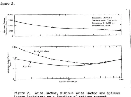
A fallacious method of optimization, and one cor.unonly used, entails finding the optimum source resistance for one value of eoitter current,
and toen optimizing IE' assuming that Rso remains constant. Figure 2
ShOHS the results obtained by both the fallacious and the prescribed optiDization procedures. The reason for the differences that exist b e-tHeen the two rr,ethods is that the optimum source resistance is an implicit function of the emitter current. This dependence is illustrated in
figure 2 .
• 10,000 r - - ---,----,--,--, -,-,,-,-,-,-,-- -- - , - -- ---,--,--.-,----,---,.-,-11r-,
~~ .. 0 7,'>00
g 0
'"
.
Op
T ... n,.J::~o.'p,o~;l, O~BC-El = -lv
-~:
,
~-:,;!
&-€
E---
F"qu",y, f. ',000 ,po:
:
:::
~----_-A ____ "-___
--6 _ _ :T.=m:p.:': .. U:,:.,~l:9S:0K~_J-'" I , I 1 1 , 1 I "
Emitter Current, ~
Figure 2. Noise Factor, Minimum Noise Factor and Optimum
Source Resistance as a function of emitter current.
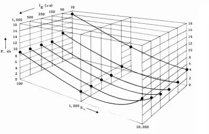
Figure
3,
Hoich applies to the same optimization problem, illustratesmore graphically the emitter-current dependence contained in R
so Tois
figure shows that, Idth an emitter current of lC\,l.a, R = 10,000 ohms; so
while with an emitter current of 1,0<X{,La, R =2.,000 ohms.
so
The solution to this optimization problem is again presented in
[image:26.545.45.471.248.564.2]18
16
14
1
I l10 F, db
8
6
4
l o
50 10
[image:27.533.42.472.66.342.2] [image:27.533.55.414.394.653.2]10,000
Figure 3. Noise Factor as Joint Function of Source Resistance
and Emitter Current.
"
• " " =
U
I,OOOL--L __ ~~L-~~~-L~ _ _ _ _ ~ _ _ ~~ _ _ ~~LU 100 8db , db 6clb Sdb 4d~ 1,000 -ldb 5db 10,000
Source Resistance Rs' ohms
18
16
14
I l
10
B
b
4
l
o
23
source resistance plane. The contours depicted are each the locus of
points, F = constant . I t is easily ShOI.Jn, by vlri ting the total differ
-ential of F, that for points on the contours that have zero slope,
R so
The trajectory contained in this figure is F
min as a function of the
emitter current. This trajectory again shows the emitter-current dependence
contained in R so
From figures 2 and 4 it is found that there is a unique solution to
the optimization problem in which the emitter current and the source re
-sistance are controllable parameters.
THE THREE FREQUENCY REGIONS
It is apparent from equation 33 that there exist for both the transis
-tor and vacuum-tube amplifier three frequency regions of interest. Since
these regions are continually referred to in the context, they are defined
at this time.
The l/f region is defined to consist of those frequencies for which
the noise factor, as given by equation 29, can be written in the form
F(f) - 1 (F - 1) -fl
o f ()8)
The mean-frequency noise region is defined to consist of those frequencies
for which
F(f) =
The f2 region is defined to consist of those frequencies for which
F( f) - 1
=
(F _1
)
(
~
)
2
o f2 (40)
Here,
R
= Ko + ~ + G R
The frequencies behleen these regions are def::'ned as transition
frequencies. The frequency dependences of the noise factor in the lower and upper transition regions are
(42)
F(f) - 1
The boun6aries of each of these regions are functions of the source
resistance. This dependence is illustrated in figure
5,
which contains curves showing the spectral character of each of the frequency-dependent,noise-factor parameters contained in equation
35.
It is found, from figure5
and equation35,
that as the source resistance approaches aninfinite value, the mean-frequency region is limited to the band f
=
30 kc to f = 200 kc, while for small values of source resistance (R - 0),s
the mean-freqllenc;, region extends from f = 2,000 cps to f = 1 mc,
" , - - -- - - - , - - ---,---,-- - - -- - , -- - - -- - - , - -- ---,
20
18-c
I
16r - 0c 0
, ,
" [0 14
c'l "
-
'1
-
, gc( x 10
S o
I
'
,8-'"
'"
R'.0
Transistor 2N43·1 Common base a.mpl
i!ie:-V CB • -LV IE • O. I rna
T t:: 29S"K
°O~.701~----~0.~I---~~--~--~~----~~~~-J~---I-"O.OOO
f:-equency. kc
25
A BRIEF DESCRIPTION OF THE THESIS
The following is a list of the chapters contained in the main body of
the dissertation, along "lith a brief resume of the contents of each chapter.
l-lEAN-FREQUENCY REGION
\'Ii th van der Ziell s noise model and the associated theory, i t becomes
possible to express the noise-factor parameters
K
o',
R no , and G nc as ex-plicit functions of the small-signal and d.c. transistor characteristics.
As a result, analytical solutions to the optimization problens can be
obtained in vlhich the source resis tance is an uncontrollable and a con
-trollable parameter. In order to verify the theoretical results, noise
rr.easurements Here made on a nu.moer of tra:Jsis tors, and the results are
given in graphical form along \<lith the predicted theoretical results. In
general, the agreement is l-lithin a decibel.
1/ f ?REQUENCY REGION
This section begins \<lith a discussion of Fonger1s l/f noise model.
With this model and the associated theory as a baSiS, it is found that the
noise-factor parameters have a frequency dependence give~ by
f
Ko' (f) '" K , 3
00
r
(44a)R (f) '" R
r
f5no noo (44b)
G (f) G f7
nc nco
r
(44c)Utilizing equations 44a, 44b, and 44c and Peterson's equivalence
theorem, it is found tha t in the lO"ler tra:Jsi tion region the frequency
K I (f)
o
R (r) no
G (f )
nc
( + ff3)
K I 1
00
G nco
(
1
+ ff7)(440)
(44e)
(44f)
Equations 44d, 44e, a:ld 441' form the basis of a simplified ex~eri;ner:ta~
solution to the optimization problem in which the source resistance and the
e;nitter current are controllable para~eters . Experimental corroboration is
given of the derived theoretical results.
Also included in this study is an analytical solution to the optimiza
-tior. problem in which the emitter current is the only controllable parame
-ter.
[{IGE-FREQUENCY REGION
To obtain a solution to the high-frequency optimization problem in
Hhich the source resistance is the only controllable parameter, it is
assumed that
a(f) =
1 + j f 'f
I c
(45a)
y (r)
e = 'J eo (l + j f/ f c ) (45'0)
Here, a(f), the common-base current gain, and y (f), the enitter-junctior.
e
admittance, are tHO parameters contained in van der Ziel1s noise model.
The solution shovls that, "lith the proper selection of the source
resistance, it is possible to obtain reasonably low noise factors up to
the a cutoff frequency, f . Experimental measurements corroborate the
c
theoretical results. Also contained in this section is a theoretica study
of the effect of source reactance on the high-frequency optimization
27
TRAI!SFORFlER COUPLING
The theoretical results obtained in section 1 reveal that a restriction
is imposed on the value of the source resistance if the optimum noise per
-formance is to be obtained. If R is not the correct value to satisfy the
s
constraint imposed by theory, it becomes necessary to interpose a trans
-former be tween the driving source and the amplifier tha t ~Iill reconcile
these differences. However, now there is a restriction on N, the turns ratio of the transforWoer. In this section, using si~plifying assumptions as to the noise added by the transforrr,er, the value for N is derived. TEf'iiPERATURE
This section contains an experimental and analytical study of the
effect of temperature on the noise performance of the transistor amplif~er.
o
The temperatures considered range from
77
to 320 K.Em'fTER DEGENERATION, BIAS STABILIZATION
In this section the effects of these two stabilizing elements on the
noise factor parameters are determined. It is assumed in making the deri
-vations that only thermal noise is generated in these elements.
~.'1 th simplif;: .. ing assUJnptlor.s as to the rela ti ve magnitude of these
resistive components, it is possible to formulate in a convenient forw. the degradation produced by their presence in the circuit.
LOAD RESISTANCE Al'm l·lULTISTAGHiG
This section contains an analytical study of the effect of the load
resistance of the first stage on the noise performance of the multistage
a;r,plifier. An expression for the noise factor of the [lUl tis tage sys tern
[fiEi,SURING V;ETHODS
An analytical description of the methods used in obtaining transistor
noise factor measurements is presented. Also L'lcluded is a method of de
29
1. r1EAN-FREQUENCY REGION
The mean-frequency region, as related to transistor-noise generation, has been defined as that portion of the frequency spectrlli~ where the sta-tistical processes responsible for the noise generated in the transistor produce a power spectral density that is independent of frequency. There-fore, in the region to be considered, l/f noise can be neglected. The
noise processes remaining are
1. Equilibrium or Johnson noise generated by the random motion of the thermally excited, charged carriers
2. Non-equilibrium noise generated by the random diffusion and
generation-recombination of the charged minority carriers in the active base region
Unlike l/f noise which is a surface phenomenon, thermal, generation -recombination, and diffusion noise are characteristic of the transistor1s
bulk properties. Therefore, it is possible to formulate the statistical
properties of the noise generated by these processes in terms of the small signal and D.C. transistor parameters.
Employing the theories of Guggenbuehl and van der Ziel that pertain to the mean-frequency region, it is possible to formulate an analytical
solution to the problem that entails optimizing the noise performance of
the transistor amplifier when both the source resistance and the emitter
;·iEAN-FREc:',UENCY NOISE HODEL
The Dean-frequency model proposed by van der Ziel and Guggenbuehl cO:lsists of tHO current generators that describe the shot-noise fluctu -ations produced by a forHard- and reverse-biased diode. Modlflcations are placed or. the magni tude of these tlo/O noise source s to account for the
zero-current thermal noise. Correlation bet,,:een the two genera tors exists through the forward transconductance of the intrinsic transistor. A third
noise source is placed in the base leg of the transistor to account for
the thermal noise generated in the extrinsic base resistance rblb. Part
a of figure 6 depicts the equivalent
"T"
representation of the mean-frequency noise model. In this rlodel, \-lith the assu111ptions that
1. There is one-dimensional current flow in the active base region 2. Drift currer.t is negligible in the active base region
,. Surface recombination is negligible
Van der Ziel found that the mear.-square fluctuation contained in the input
and output current could be described by
*
i 2 nl
i i
nl n2
"""2
e!'1b
4kTR1y )B - 2eI B ·W e E
2kTy ec iB
(l-la)
(l-lb)
(l-lc)
(1-1d)
Part b of figure 6 depicts a simplified equivalent representation of
the :nean-frequency noise model. In this figure,
e
31
i i
n2 - ai
nc nl
In the simplified rr.odel, i f it is assUI:1ed that
iJ.Vcbl 0 (1-4)
eI E
Ye kT
(
1
-
5)
and
Ie a o-E T + leo (1-6 ) i t follo\·/s, froD equations l-la to 1-6, that the generators Hill ;1ave
Dean-square values given by
i2 nc
""2 e
ne
=
2kTr B e
Hhere r e is the s~all-signal, e~itter-junction resistance (r e
(1-7a)
(1-7b)
(1-7c) l/Y e ).
The advantage of the sir;.plifieci model is that the correlation that formerly existed bett-Jeen the tvlO current noise sources (contained in the original model) is now zero, i . e . , e
*
ine nc =
o
.
It is evident, from equations l-7a to 1-7d, that the noise performance
of the transistor amplifier can be expressed in terp.s of measurable d.c.
and small-signal paraweters. These parameters are rbta the ext::,insic base resistance I = the collector cutoff current
co
IE the eoitter current
ia)
R
s
(b)
Figure
6.
Representation of Transistor Mean-Frequency Noise Model: (a) Current Source inl
in Parallel with r
e, (b) Voltage Source ene
in Series with r .
e
,
no32
COENON-BASE AND CONr,:ON-EIUTTER A?'iPLIFIEflS
It fo11o\-/s, from figure 1-2 and equations 1-7a to 1-7d, that the ;-wise
factor of the connon-base arr.plifier is
F (1-8)
For the common-emitter arr;plifier, the noise factor becomes
r rblb
(
T
I
Zc
l
2 .,.
e~e
)( Rs + r + rbl J 2
F 1 ... 2R e + -R- + nc e
(
1
-
9)
4kTR Ib: 21z _ :e12
s s
s o c 0
}lnere z = I/Y .
c c
At mean frequenc:es, u~der normal biasing conditions, the collector
i;';Jpedance, z , is usually greater than 100,000 oilr:",s. Therefore, it is safe c
to assume that
z
»
reI b/aoc 0 -10)
I
Z cl2 2rb1bre
»
ao(l-ao)
(1-11)
2r 2
I
Zcl
2 e
»
ao(l-a o)(1-12 )
Prom equations 1-5 to 1-12, the noise factor of the cor:1IIOn-base and
of the comDon-emi t ter transis tor stage can nOH be }rri tten
He!"e, ~ is the cor.m,on-enitter cu::'rent Gain,
1 - 0:
o
and
r
is the collec"Cor cutoff-curre!'1t noise paraneter,r
It is seen from the foregoing equation that
r
is a function of theenitter current . Typical values of this parar~eter (sho\,n: in Tables 1-1,
1-2, and 1-3) varj' frorr, 6 \-lith IE = lC1.ta to 0.3 with L = lr.1a.
~
In order to facilitate the analysis of the noise-optimization proble~,
ir. Hhich both the source resista:1ce and the emitter current are tile COD
-trollable parameters, it is again possible to express the noise factor in
terms of the three noise fac tor parameters (equa tioD 24), i.e.,
F
R
no
= Ko + R
s
+ G nc s R (1-14)
It fo11oHs, fror~ equations 1-13 and 1-14, that for the corr4"'lon-base
and cO:nr.1on-emitter amplifier
R
no
G nc - -1 (1 +
n
2f3r e
(1-15a)
(1-15b)
(1-15c)
substituting the values for the noise factor parameters Eiven by
equations l-15a, 1-15b, and 1-15c into equations 25a and 25b, the optir:.uli.
R so
1
F . = 1 + - -- (1 .;-,..) (r + r. ,. )
Inn f3re e : : > 0
The !:linir:luJ:1 noise factor, F nan . , is an implicit function of the
(1-16)
emitter current.* Therefore, the solution to the opti~!zation problec
in which both the source resistance and the emitter current are controlla
-ble oarar:leters entails differe:ltiating F. I-lith respect to the er.-,itter
. rnn
current and equating the resultinE differential to zero. If it is assu~ed
o
(I-IS)(1-19)
and
(1-20)
the result 0:' this differentiation yields for the optil1lUF.! emitter current
0 -21 )
If the restriction imposed by equation 1-20 is re!':oved, the optimwr, r
eDitter current lies betHeen l1r:lits that differ by a factor of the \12.
*This depe:ldence ca:l be n:ade explicit ,-ii th the equation IE = kT
These l1mi ts are
k'$I CO )1/2 I
~
k'$I
CO )1/2, 2erb1b < EO < erb1b (1-22 ) From equations 1-16 and 1-21, the opti~al source resistance (Rso)o
becomes
rb1b
r
2 Jl/2 = - - , (2 + r) + 4f3r
L
If it is assumed that
equation 1-23 simplifies to
t3I CO) 2 + 202 1
o E
= 2rblb
~1
/
2
r
(1-24 )Equations 1-21 and 1-24 apply to the common-base and common-emitter amplifier opera ted in the nea:1-frequency region. These tHo equations shol-I that it is possible to solve the :1oise opti~ization problem in which both the source resistance and the enitter current are controllable parameters without making noise measurements .£!2 the a:npl1f1er.
cor';JfJON-COLLECTOn Al>lP1IFIER
The noise factor of the common-collector amplifier, derivable from equations 1-7a to 1-7d, becomes
F r/2l Rs + rb1b
Rslzcl2
+ z
12
12
(R + r _)2c + ?c s biD
- -2
! r + (1 - ex )(R + r-01b)J'
L e o s
+
---~~~---Rs RL
4k'l'R B
s
vii th typical values for load resis tance (R
L = 10,000 OMS), emit ter
jU!'1ctlon resistance (re
=
26 ohrr,s ), collector impedance (zc=
1000,000onr.ls), a!')d sDall-signal current gai!') (() = 60), i t can safely be asswr,ed that
RL
»
2re1/2
z » ( ) r
c e
2t3r2
1 z c
12
»~_(l + r) e-,,::-;Hith these assmnptions equation 1-25 can be simplified to read
F = 1 +
(1-26)
(1-27 )
(1-25)
(1-29 )
(1-30)
An analysis sinilar to that carried out for the cOr.l.lIon-base ampli -fier yields as the optimizing parameters for the cor.~on-collector stage
(1-31)
(1-32 )
EXPERII-iEt,fTAL l'IEASUREi·!ElITS
In order to establish the validity of the assu~ptions made in derivin~
ti1e equations contained in th:'s sectio!'), and in crder to establish toe validi ty of toe equations themse 1 ves, :near.-frequenc~' noise r.,easurements Here made on a large group of alloy, micro-alloy, and diffused base
transistors. For each transistor tested, wito the operating point fixed, r.oise-fac tor measurements .. 'ere :nade wi th several discrete values of source
drawn to obtain exper:~e~ta- values for the op&im1zi~-~ . Dara~eters Rso and
F . • This procedure Has repeated '.·:1tn the err.:tter current as the inde
-T:'i:' n
pendent variable. For each tranSistor tested, a curve was plotted to depict
F . and R as a func t10;'] of the emi t tel' current. A partial co!:',pila t!..or. of
1'-ln so
the experi~ental results is co~tained in the three parts of figure
7
.
In order to obtain theoretical curves showing F_1 and R as a
,.I~n so
function of the emitter curren&, measure:nents Here !:lade of
le
o
'
t3, andrbtb. From these measurements and equations 1-16 and 1-17, the theoretical
curves shown in figure
7
were drawn. The theoretical results are also givenin Tables 1-1, 1-2, and 1-3.
A cO:'1parison of the theoretical and experime!1tal results reveals that
for frequencies above a f'el-l kilocycles, the theoretical model forms a valid
basiS for obtaining the optimization parameters of the ar.;plifier.
For tne 2N207-B tranSistor (characteristics shoH/; in part a of figure 'r)
tne theoretical optimum emitter current was found to be 87 ~a; experimen
-tallJ', the value 100 ~a ,-;as obtained. For the 21'143 transistor (part b of
figure 7) the theoretical value obtained ~!aS 450 ~a, and the experirr,ental
value 200 ~a. For the 2K544 tra:lsis tor (part c of figure 7), the theore ti
-cal value is 350 ua; tne experimental value is 200 ua.
SOURCE RESISTAiJCE AS Ali UliCONTROLLABLE PAHAHETER
Equations 1-21 and 1-24 quantify the e!:'.itter current and the source
resista:lce that give the optimur.] noise perforrr.ance for a Biven tranSistor.
Because the optimal source resistance can be rr.odified by the use of a
transformer at the input of the arr.plifier, a wide latitucie exists for the
source resistance that Hill satisfy the constraint ir.,posed by equation 1-24.
However, in rrany cases, it is found that other considerations prohibit
"
"
< ;
.;
.
• <
'" ;; " 0
·
• . 07,500
2Nl07B-Z Transistor
Common ~mitter amplifier
VeE:: -Zv T = Z9S·K
~
iii-.
,~
..
:
~ " c"
·
:1·
•..
·
·
cZ C , E < ~ .~ ~o: E E i'i. o
0 - Experimental measuremenU £ :: O. 006 me
X - Measurements at £ = O. 006 me with
J
-4 ~ 6 - ~~p::::e:~~::~.urement. f = 0.02
me
,
I Theoretical resulta
1
:} tEO
f
J
---__
~
h
~
0---r
J
---.
,+-L-" - -..i
10
3,000
100
Emitter Current IE'
(a)
ZN4)-l Transistor
VeE'" -lv T . 29S"K
I, 000
0 - - Experiznental mealurements f c O. OOb me
x- - Measul'ementa at f ;:; O. 006 me with Iff noise removed
_ _ _ Thf:oreticai results
I ••
Emitter Current IE'
(b)
o
lEO x
, u
c <
.~
.
4.00°
1
-1
~o 3,000i
lN544 -1 Tranalltor
Common Emitter Amplifier
VeE:: _z... T:: 195·K
ict.
-
z.OOO
i
i
',OO:L[ _______ L - _ - L __ _ L _ _L-~~
~_L
_ __ _ _ _ _ L _ _ _ _ L _ __L~L_~~~~
~ ~ ~ E
..
·
6s
~
4 o"
Experlmer.tal measurement. (I :: 0.006 md
Experimental meaSUrements (f :: 0.5 me)
Theoretica.l results
f
1
l
·
..
u·
<;z § E ;; ~ 10
7.
o"
100 (c) o ci
i
I. 000
Minimum Noise Factor and Optimum Figure
Source Resistance as Function of Emitter
Cur-rent (a) Low-Noise Alloy-Junction TranSistor,
Table 1-1. Theoretical i·leasure of the Noise Pararleters as a
?unction of Er.:itter Current for ~he 2N207-B Tra~sistor.
Trar.sistor IE' ;·iicroa~nperes 21~2073
i'lo.4- 10 50 100 200 500 1,000
K 1.14 1.06
0 1.06 1.10 1.09 loll
R
no' oh:::s 2,160 700 550 445 360 350
G nc , )o'mhoR 4-4 52 66 88 130 150
r
6.0 2.8 1.0 1.3 0.6 0.34F nin' db 2.3 1.6 1.6 1.7 1.8 2.0
R
so' ohn~s 6,950 3,600 2,900 2,300 1,920 1,520
Taole 1-2. Theoretical Jo1easure of the Noise Para!'1eters as a Function 0:' Emitter Current for the 2N43 Transistor.
Transistor I~, :·jicroar.lperes
L'.
2N43
No.1 10 50 100 200 500 1,000
K 1.6 1.4
0 1.2 1.2 1.2 1.2
R
no' ohr:JS 2,500 650 370 260 230 100
Gnc' y!~lhos 380 240 250 300 380 570
r
5·2 5.1 2.3 1.4 0.8 0.6F
!:lin' db 5·7 5.2 2·7 2.3 2.1 2.5
R
[image:45.548.50.468.111.343.2]1;.0
Table 1-3. Theore tical l'·ieasure of the j·loise Fara",e tel'S as a
FU!1c tio:'] of Err. i t ter Current for the 21:544 Transis tor .
Transistor IE' :'iicroa:nperes
2Ji5!~4
1 10 50 100 200 500 1,000
i<
0 1.50 1.10 L ob 1.05 1.05 1.05
fl
no' ohJ~!s 2,600 600 410 280 130 90
G
nc' ~mhos 120 62 75 96 150 240
r
2.1 2.1 1.3 0.5 0.4 0.3'"
. min' db 1.& 1.6 1.7 1.2 1.2 1.2
R
so' ohr.lS 4,600 3,100 2,400 1,600 890 600
dictated scurce resista!1ce Hill, in general, not satlsfy equation 1-24.
OptiDizatlon, in this case, entails finding the eDitter curre~t that oini
-;r.izes the noise factor of ;;he amplifier. I t can be found by differentiating
the noise factor \-li th respect to the er.litter curre:'lt and equating the re
-sulti:1g differential to zero. ?or the corr~on-base and comnon-emitter
a:.1plifier, i f it is asslL'11ed that
~
»
2
r
+1
(1-33 )the optimurr. emitter current is giver. by
(I-34 )
?or the comnon-collector amplifier
= (1-35)
In order to corroborate equation 1-34, r.oise c,easurements \-Iere clade
figure 2; as \·;ell as the theoretic<J.1 results obtaineci with equation 1-34.
The correspondence shows that, for ~requencies above a few kilocycles,
equation 1-34 forns a valid basis for the solution of the optimization
probler;] in Hhich the err.i t ter current is the only cO:1trollable paralr,e ter.
E~UIVALENT !'WISE RESISTAI;CE
The equivalent no2.se resistance can be used to illustrate the degra
-da:ion in the noise perforl'"lance causeci by each of the noise generators
contained in the mean-frequency model (part b of figure 6). This parameter defined 0;"
R eq {F - l)R
s
beco::les for the cormnon-baso and comr:lon-emi tter transis tor a~lplifier
Hhere
R
r e /2
rblb
1 +
r
2f3r e
eq
the
the
2
re/2 + rblb + (I + r) (Rs + rblb + re)
2f3r
degraciation
degradation
e
caused by e ne
caused by e nb
the degradation caused by i
nc
:.'igure 9 illustrates the relative oagnitude of each term of
(1-36)
equation 1-36 as a function of the source resistance and the experimentally obtained curve shoHing -.;he equivalent noise resistance as a function of the
source resistance.
COLLECTOR VOLTAGE AND ITS EFFECT ON i·SAN-FREQUEHCY NOISE PERFORiflANCE
An inspection ot the equations that dictate the noise performance
of the tra:1sis tor anplifier in the lLeal:-frequency region reveals that,
theoretically, the collector voltage is a noise para~eter in a transistor
stage only because of its influence on ~ and z at low reverse biases,
~
"
16.... 14
O
z
8
42
2NZ07B-2. Transistor
VCE = .Zv T = Z9S'K
R. = 100 f = 6, 000 cps
Theoretical value for lEO
; 10 t
-o ________ -L ____ -L __ _ L _ _ ~_L_i_i,_L,~, _ __ __ _ _ _ ~L_ _ _ ~L ___ L_~ _ _ L_~L_LJ
10 1,000
(a)
10r---r----.---.--.--r-r-r.-.---,---.---.--.--.-r-r~
2~207B-2 Transistor
u:
VCE = ·Zv T = Z9S'K
Rs=l,OOO f=6,OOO cps
~8~
~ : Theoretlca1 value for l E O \
~--~v---~---~---~
v
·
'0 z Z
, I
10 100
IE' /la
1,000
10
~ 8
'0
~ ,.; 6
3 u
•
4...
•
" '0 2
z
0 10
Figure (a) R
s
Theoretical value for lEO
(b)
2N2.07B-2. Transistor
Common emitter amplifier
V CE = ·Zv T = Z9S'K
Rs = 10,000 f = 6,000 cps
(c)
1,000
8. Noise Factor As Function of Emitter
~ 100 ohms, (b) R = 1,000 ohms, (c) R
s s
Current with:
·
E~
"g" I 4
a: 0
·
'< "<
·
·
X
·
·
oZ c , -.
{ ::; 6. 000 cps T '" 295 K
~ 103
--1 - - - -- -
-zl,CO-_ _ _
10100
r
.
/2.\
\
,
L,OOO
I I ' _ J
SOl!rce Re$';'Ma.:l.ce R , , ohms
10.000 '50. 000
Figure
9.
Equivalent Noise Resistance as a Function of Source Resistance.and its influence on
leo
at high reverse biases. In order to obtain anexperimental verification of the theory, noise studies were p.iade on several
transistors with the collector voltage as the only independent parameter. The results of these measurements revealed that although the noise level
observed at the output of the transistor stage decreased sharply as zero
biasing was approached, the decrease in the pO'vler gain offset any advantage
produced by the lOHer noise level. At the other extreme, as the collector
breakdovJn voltage Has approached, a perceptible increase in the nOise level was observed. HOyleVer, with collector voltages ylithin the range 0.25 v to 10 v reverse bias, little change Has observed in either the noise