Design of three-component one-dimensional photonic crystals for
alteration of optical contrast and omni-directional reflection
Anna V. Baldycheva
a, Vladimir A. Tolmachev
b, Tatiana S. Perova
*aand Kevin Berwick
ca
Department of Electronic and Electrical Engineering, Trinity College Dublin, Dublin 2, Ireland;
b
Ioffe Physical Technical Institute, Polytechnicheskaya 26, St. Petersburg, Russia;
c
Department of Electronic and Communications Engineering, Dublin Institute of Technology, Kevin
St, Dublin 8, Ireland
ABSTRACT
In this study, three-component One-Dimensional (1D) Photonic Crystal (PC) structures were investigated by modeling them as two-component PCs with an additional regular layer. The Gap Map approach and the Transfer Matrix Method were used in order to mathematically describe these structures. The introduction of a third component to a 1D PC allows manipulation of the optical contrast to a high degree of precision by varying the thickness and refractive index of the additional layer. It also partially reduces the area of the photonic band gaps (PBGs) on the gap map, leaving the remainder of the PBG area unchanged from that of the gap map for the original, two-component, PC. Using this approach to decrease the optical contrast in photonic crystals allows omni-directional bands to be obtained in high-contrast periodic structures constructed from, for example, an array of silicon and air.
Keywords: 1D Photonic Сrystal, Tunable Photonic Сrystal, Multi-component Photonic Сrystal, Photonic Band Gap, Photonic Gap Map
1.
INTRODUCTION
Photonic Crystals (PCs) 1, 2 have attracted considerable scientific and commercial interest in recent decades because of
their unique properties in manipulating light. Photonic Crystals exhibit total reflection over a range of frequencies, that is, they have a Photonic Band Gap (PBG). Optical devices based on multi-dimensional PCs can be used to fabricate numerous optical elements, including waveguides, reflectors, attenuators of spontaneous atomic emission and devices for controlling emissions in micro-cavities1-3. These devices operate by the PBG effect and, therefore, possess high
sensitivity to the refractive indices, N, of their components. Manipulation of N allows the design of PBG materials whose optical characteristics can be varied over a wide range. The PCs are normally composed of two-components, with high (NH) and low (NL) refractive indices. By changing the value of NH or NL, tuning of the PBG position can be achieved. One of the most promising high-refractive indexes, (H) materials is Si, due to its low-cost and ready availability. However, the variation of the refractive index, NH, of Si by heating, or free carrier generation, is minimal (∆NSi=0.001). At the same time, variation of the low-refractive index component, NL, has a far greater impact on the PBG shift. In order to change the value of NL, i.e. to decrease or increase the optical contrast, the air-gaps, or channels, can be impregnated with various liquid or solid fillers. A number of studies were published recently on the infiltration of air-channels with Liquid Crystals (LCs), which enables tuning of the optical contrast due to reorientation of the LC molecules4. Typical
liquid crystals used for device applications have refractive indices in the range 1.5 to 1.8. Although this technique is technologically well developed, there is an alternative approach to engineering the PBG.
*[email protected]; phone 3 531 896-1432; fax 3 531 677-2442; http://www.mee.tcd.ie
Photonic Crystal Materials and Devices IX, edited by Hernán R. Míguez, Sergei G. Romanov, Lucio Claudio Andreani, Christian Seassal, Proc. of SPIE Vol. 7713, 771321
© 2010 SPIE · CCC code: 0277-786X/10/$18 · doi: 10.1117/12.854977
Proc. of SPIE Vol. 7713 771321-1
This approach requires the introduction of an additional component to the PC, forming a three-component PC. It is worthwhile to refer to recent investigations of multi-component, 1D and 2D PCs5, 6. The authors of Ref.6 have shown,
based on the example of 2D PCs, a shift of the gaps’ edges. This shift depends on the thickness and dielectric constant of the intermediate layer on the surface of the cylindrical pores. They explained that the shift is associated with a decrease in the effective dielectric constant of the system. The authors of another paper7 studied a multi-component
model for a more complex, 3D PC structure, and have shown, based on an opal structure sample, that it is possible to selectively manipulate the PBGs in this PC. They have demonstrated the possibility of controlling the emergence of the PBG, along with the width and spectral shift, and also digital ON/OFF switching, by varying the additional layer’s thickness, permittivity and other parameters in the multi-component PC.
In our paper 8, we selected the 1D PC as the simplest example for calculations, as well as for demonstrating PBG
modification, in both position and width, due to the introduction of an additional regular t-layer. We have analysed the properties of a three-component PC structure based on a Gap Map (GM) approach3. As demonstrated earlier, the GM
method is a very efficient approach for the analysis of both tunable9 and composite 1D PCs10, as well as for PC structures
with omni-directional bands and defects11.
Over the last decade, particular attention has been paid to the development of devices based on one-dimensional PCs, since they possess certain advantages over two- and three-dimensional PCs. These advantages are mainly related to their simpler fabrication, lower cost, and the possibility of creating omni-directional bands (ODBs) 12-14. Calculations of the
optical properties of 1D PCs with ODBs must take into account the refractive index contrast (or optical contrast) NH/NL, which should be large if one wants to achieve a maximal PBG width. It should also be noted that photonic structures with an optical contrast that is too large have the disadvantage that closure of the PBGs can occur at particular angles of incidence of light and, therefore, result in the disappearance of the ODBs for the structure. In accordance with 3,13, the
minimum value of NL should be greater than 1.1 for light incident from air. As a result, it is impossible to obtain ODBs for structures with a high-optical contrast, such as grooved Si with contrast 3.42/1 which can be used as a 1D PC material in the infrared (IR) range15. At the same time the introduction of the additional layer with a particular optical
thickness into high-contrast PC can, under some conditions, results in creation of omni-directional bands. In the present paper, our investigations are focused on PCs with a variety of optical contrasts, as well as for different angles and polarisations of the incident light. Particular attention is paid here to the tuning of the optical contrast in 1D PCs.
2.
RESULTS AND DISCUSSION
2.1 Modeling of three-component photonic crystal structure
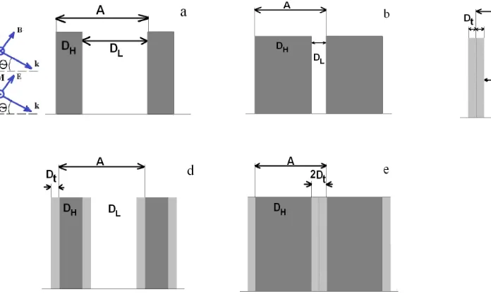
A periodic structure with linear grooves on the micro scale16 is considered here as a model for a 1D PC structure (Fig.1).
This consists of alternating layers of material with high, NH, and low, NL, refractive indices. The refractive index of Si for the H component in the IR range is chosen as NSi=NH=3.42. The refractive index of air for the L component is Nair=NL=1. In this case, the refractive index contrast is ∆N=NH/NL=3.42/1 and the PC obtained can be considered a high-optical contrast PC. Therefore, only a small number of periods m are required to obtain a PBG with a reflection of greater than 0.999. Let us consider two examples of this 1D PC with the number of periods m=5 and m=10. We would like to investigate the impact on the PBGs caused by insertion of an additional regular layer such as, for example, SiO2
with a refractive index Nt =1.5, which can be deposited on the Si walls of the 1D PC structure with a definite lattice constant, A. The refractive index of the incoming and outgoing medium, N, is taken as N=1. All the optical characteristics presented in this study utilize normalized frequency NF=A/λ units and, therefore, can be applied to a wide range of structure sizes, including micro- and nano-structures.
Calculations of the reflection and transmission spectra of 1D PCs with a number of lattice periods, m, and a filling fraction of the Si walls fSi=DH/A, can be performed using the Transfer-Matrix Method (TMM)17. This method is attractive due to the ease of introduction of an arbitrary number of additional layers at any point in the TMM’s equation (Eqs. (1) and (2)).
Proc. of SPIE Vol. 7713 771321-2
Fig.1. Schematic fragments of (a, b, с, e) two-component 1D PC and (d) three-component 1D PC with fixed value of lattice constant А and an additional t-layer. The thicknesses of H, L and t layers are DН, DL, Dt, accordingly.
The Transfer Matrix, S2, used in calculations for a two-component 1D PC structure, is given schematically by:
for a three-component PC matrix, S3, as shown in Fig.1d, the matrix is8: S3=( Mt ·MH ·Mt ·ML) m·Mt ·MH·Mt , (2)
where MH, ML and Mtare the matrices of the H, L and t layers, respectively.
Indeed, the reflectance spectra obtained for different filling fraction, fSi, values can reveal significant differences in PBG formation5. As demonstrated earlier, the best analysis of the optical properties of PC structures is obtained using a
combination of TMM and GM approaches9, 10, 18-20.
The GM approach enables us to choose the parameters required for the engineering of 1D PCs based on grooved Si 16. In
[image:3.612.102.450.75.285.2]particular, we can identify the range of frequencies that can be practically realized for these structures, and, therefore, establish the design criteria for different regions of the IR spectrum.
Table 1. Maximum value of filling fraction LimfSi for different values of t-layer thickness, Dt , required for GM calculations of a three-component PC with lattice period A.
Dt 0.03A 0.07A 0.10A 0.13A 0.20A 0.27A 0.33A 0.40A 0.47A
LimfSi 0.94 0.86 0.80 0.74 0.60 0.46 0.34 0.20 0.06
In order to create a GM of PBGs we need to generate the set of reflection spectra for each value of the filling fraction
fSi=DH/A ranging from 0 to 1. Next, values of frequency satisfying the required criterion for PBG formation (R>0.999) are selected. We assume that the lattice constant A and the t-layer thickness, Dt,do not change, since the t-layers with refractive index Nt were introduced on both sides of the Si wall H in our PC structure (Fig. 1d). When generating fSi, the values of DH for both two-component and the three-component PCs are the same and, therefore, we can compare two different PC structures using a single fSi scale. However, in this case, the value of DL decreases after the introduction of the t-layer with thickness Dton both sides of the Si walls DH (Fig.1d). As a result, when plotting the GM, not all values for the filling fraction fSi, from 0.01 to 0.99 can be realized in practice. The larger the value of Dt, the lower the
S2=(MH·ML) m·MH , (1)
Proc. of SPIE Vol. 7713 771321-3
[image:3.612.97.513.558.595.2]maximum value of the filling fraction fSithat can be realized in the three-component PC. In Table 1, the maximum values of the filling fractions fSi, obtained for different values of the t-layer thickness Dt, are presented.
2.2 Engineering of the optical contrast of a three-component photonic crystal structure
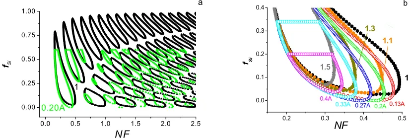
Let us calculate the GMs of the PBG for a three-component PC with number of periods m=10, obtained by the introduction of a t-layer with various thicknesses Dt (Table 1) into a two-component PC with high optical contrast N=3.42/1 (Fig 2, Curve 1). For comparison purposes, we will also calculate the GM for the limiting case, when the L -component is totally replaced by the t-layer and we obtain a two-component PC with medium optical contrast
N=3.42/1.5 (Fig 2 b, curve 1.5).
0.0 0.5 1.0 1.5 2.0 2.5
0.00 0.25 0.50 0.75 1.00
a
fSi
NF
1
0.20A
0.2 0.3 0.4 0.5
0.0 0.1 0.2 0.3 0.4
1
1.1 1.3
f Si
NF
1.5
0.2A
0.27A
0.33A
0.4A
b
[image:4.612.98.511.217.358.2]0.13A
Fig.2. a) The GMs for two-component PC with optical contrasts N=3.42/1 (1) and for three-component PC with t-layer with Nt=1.5 and Dt =0.20A (0.20A) in a wide range of NF. b) Comparison of the lowest PBGs for three-component PC with various thicknesses Dt and two-component PCs with different optical contrasts (3.42/1, 3.42/1.1, 3.42/1.3 and 3.42/1.5), shown by numbers beside the curves. The normal incidence of light is considered here.
Figure 2a shows that the introduction of a t-layer with Dt =0.20A and Nt =1.5 results in i) a decrease in the size of all PBGs and ii) a red shift of the PBGs with respect to the original two-component PC. Similar behavior was observed earlier in the GM of the PBGs of a two-component PC as NL increases9, 15. Thus, the introduction of the t-layer has a similar effect to the substitution of NL, i.e. it serves to decrease the optical contrast or, in accordance with Ref.6, decrease the effective dielectric constant. As can be seen in Fig. 2a, the size of the high-order PBG regions for the three-component PCs differs from that in two-three-component PCs.In the range of NF values from 0.7 to 1, a suppression of high order PBGs takes place.
It can be also be seen in Fig. 2 b that the blue edges of the first PBG, for NL=1.1 and 1.3 for the two-component PC, intersect the blue edges for the three-component PC at f=0.2, with Dt =0.13A and 0.27A. Therefore, the addition of the new layer to form the three-component PC has an impact on the PBG of the crystal, demonstrating the possibility of manipulating the optical contrast by changing the thickness of the additional regular layer in the PC structure. In other words, the Dt value provides an equivalent value of NLequ for a two-component PC with the same NH value.
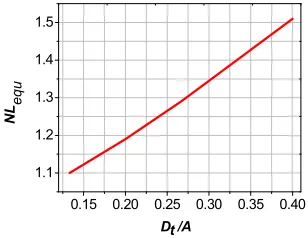
From Fig. 3, for the chosen value of Dt, the range of NLequ can be varied from 1.1 to 1.5 (in the limiting case), where the
L-component is totally replaced by SiO2 and we have a two-component PC with a contrast of 3.42/1.5. As discussed
earlier, modification of the optical contrast is possible by changing the thickness of the additional layer Dt. Changing the refractive index Ntis an alternative method of modifying the optical contrast and, like Dt, the value of Ntcan be altered technologically. So, by changing the values of Dt·Nt for the t-layer in the interference structure, new types of PC structures with optical contrasts from 3.42/1 to 3.42/1.5 can be designed.
2.3 Formation of omni-directional band in a three-component photonic crystal structure
It is well known that the ODB is normally determined by overlapping of the regions of high reflectivity for both polarisations and all angles, θ, of the incident light3. However, it was already shown that an ODB cannot be obtained,
Proc. of SPIE Vol. 7713 771321-4
regardless of filling fraction, for 1D PC structures with a value of NL less than 1.124. As mentioned in the section 2.2, we can easily change the optical contrast of a PC by introducing a third layer. Let us now calculate the transmission spectra for various, three-component, PC structures with different Dt values, over a range of possible angles of incidence from 0 o to 85o, with a step size of 5o (Fig. 4). The width of the PBGs for TE polarization increases with an increase in θ, while
for TM polarisation it decreases. As a rule, it is necessary to ensure that the PBGs for TM polarisation have a common
0.15 0.20 0.25 0.30 0.35 0.40 1.1 1.2 1.3 1.4 1.5 NL equ Dt /A
Fig.3. The refractive index of the low component in the equivalent two-component PC NLequvs. the t-layer thickness over lattice period A of three-component PC with refractive index Nt=1.5.
area for different θ in order for this area to be identified as the ODB. Figure 4 shows T spectra for a three-component PC with various Dt and also for the equivalent two-component PC, obtained for TM polarization. Note that we concentrate on the lowest PBGs and, for clarity, only two limiting cases for the incident angle, θ=0o and θ=85o, are
shown. The common ODB areas are depicted by the rectangles. For comparison, Fig. 4a shows the spectra of a two-component PC with a contrast of 3.42/1.
0.2 0.3 0.4 0.5
1E-12 1E-10 1E-8 1E-6 1E-4 0.01 1 00 3comp a 2comp 85o 00 T NF 85o
0.2 0.3 0.4 0.5
[image:5.612.228.382.166.285.2]1E-10 1E-8 1E-6 1E-4 0.01 1 85o 0o 85o b T NF 3comp 2comp
Fig. 4. The ODB’s width (filled rectangles) and the transmission spectra T for the first PBGs at incident angles of 0o and
85o for two-component PC (denoted as 2comp) with optical contrasts (a) 3.42/1 and (b) 3.42/1.3, and three-component
PC (denoted as 3comp) with an additional layer Nt=1.5 and (a) Dt=0.2Аand (b) Dt=0.27А. The limiting filling fraction LimfSi value is 0.3. The dashed line corresponds to the level of RPBG=0.999 (or TPBG =0.001).
This structure does not form an ODB, since there is no overlapping of the PBGs for angles of incidence of 0 and 85o, see
the curves corresponding to 0o and 85o for the 2comp case on the plot. Observe that the introduction of a t-layer with D
t =0.20A results in overlapping of thePBGsand leads to the formation of an ODB area. A similar effect can be observed for the structure with Dt =0.27A (see Figs. 4b). However, the degradation in the T-bands is observed for an angle of incidence θ = 85o, but it does not lead to a decrease in the width of the ODB area. On the contrary, the ODB width for
the three-component PC is wider than that for the equivalent, two-component PC. We conclude that the introduction of the additional, regular layer into a high optical contrast PC, for example 3.42/1, is equivalent to the substitution of a low-refractive index component, L, a process which results in the appearance of ODBs.
Proc. of SPIE Vol. 7713 771321-5
[image:5.612.103.500.406.536.2]3.
CONCLUSION
In this paper, three-component 1D PC structures were investigated by modeling them as two-component PCs with an additional regular t-layer. The Gap Map approach and the Transfer Matrix Method were used in order to mathematically describe these PC structures. Introduction of the third component allows variation of the PBG areas of the three-component PC and, therefore, engineering of the optical contrast of the original two-three-component PC. This can be achieved, not by filling the air channels of a two-component PC, but by selecting either the thickness or refractive index of the third component. Using this approach, omni-directional bands can be obtained in high-contrast Si-air periodic structures.
Acknowledgments
This work has been supported by the ICGEE Programme (funded by IRCSET, Ireland) and Grants from the Russian Foundation for Basic Research, N08-02-01408 and 09-02-00782. The authors wish to express their appreciation to Dr. Ekaterina Astrova for useful discussions and to Ms. Claire Poinsot for her help with the calculations. Anna Baldycheva acknowledges SPIE Travel Award.
REFERENCES
[1] Yablonovitch, E., “Inhibited Spontaneous Emission in Solid-State Physics and Electronics,” Phys. Rev. Lett. 58(20), 2059-2062 (1987).
[2] John, S., “Strong localization of photons in certain disordered dielectric superlattices,”Phys.Rev.Lett., 58(23), 2486-2489 (1987).
[3] Joannopoulos, J.D., Meade, R.D., Winn, R.D., [Photonic Crystals], Princeton University Press, P.184, (1995). Joannopoulos, J.D., Winn, S.G., Meade, R.D., [Photonic Crystals. Molding the Flow of Light], 2nd ed., Princeton University Press, (2008).
[4] Busch, K., Lölkes, S., Wehrspohn, R., Főll, H., [Photonic Crystals. Advances in Design, Fabrication, and Characterization], Weinheim: Wiley-VCH (2004).
[5] Yi, Zh. and Qi, W.,“Properties of photonic bandgap in one-dimensional multicomponent photonic crystal”, Optoelectronics Lett., 2(1), 15 (2006).
[6] Glushko, A., Karachevtseva, L., “PBG properties of three-component 2D photonic crystals”, Photon. Nanostruct., 4, 141-145 (2006).
[7] Rybin, M.V., Baryshev, A.V., Khanikaev, A.B., Inoue, M., Samusev, K.B., Sel’kin, A.V., Yushin, G. and Limonov, M.F., “Selective manipulation of stop-bands in multi-component photonic crystals: Opals as an example”, Phys. Rev. B. 77, 205106 (2008).
[8] Tolmachev, V.A., Baldycheva, А.V., Krutkova, E.Yu., Perova, T.S. and Berwick, K., “Optical characteristics of a one-dimensional photonic crystal with an additional regular layer”, Proc. of SPIE, 7390, 739017 (2009). [9] Tolmachev, V. A., Perova, T. S. and Berwick, K.,“Design criteria and optical characteristics of one-dimensional
photonic crystals based on periodically grooved silicon,” Appl. Opt., 42, 5679-5683 (2003).
[10]Tolmachev, V.A., Perova, T.S.and Moore, R.A., “Method of construction of composite one-dimensional photonic crystal with extended photonic band gaps,” Opt. Express, 13(21), 8433-8441 (2005).
[11]Tolmachev, V., Perova, T., Krutkova, E., Khokhlova, E., “Elaboration of the gap map method for the design and analysis of one-dimensional photonic crystal structures”, Physica E: Low-dimensional Systems and Nanostructures, 41, 1122-1126 (2009).
[12]Fink, Y., Winn, J.N., Shanhui, F., Chiping, C., Kimerling, L.C., “A dielectric omni-directional reflector”, IEEE J. Sel. Top. Quantum Electron, 12, 1345 (2006).
[13]Chigrin, D.N., Lavrinenko, A.V., Yarotsky, D.A., Gaponenko, S.V., “Observation of total omnidirectional reflection from a one-dimensional dielectric lattice,” Appl.Phys. A, 68, 25-28 (1999).
[14]Russell, P.St.J., Tredwell, S., Roberts, P.J., “Full photonic bandgaps and spontaneous emission control in 1D multilayer dielectric structures,” Opt.Commun., 160, 66-71 (1999).
[15]Perova, T.S., Tolmachev, V.A., Astrova, E.V., “Tunable photonic structures based on silicon and liquid crystals”, Proc. of SPIE, 6801, 68010W1 (2008).
Proc. of SPIE Vol. 7713 771321-6
[16]Tolmachev, V. A., Astrova, E. V., Pilyugina, Yu. A., Perova, T. S., Moore, R. A. and Vij, J. K. “1D photonic crystal fabricated by wet etching of silicon”, Optical Materials, 28(5) 831-835 (2005).
[17]Azzam, R. M. A., Bashara, N. M., [Ellipsometry and polarized light], Amsterdam, North-Holland, P.334 (1977).
[18]Tolmachev, V. A., Astrova, E.V., Perova, T.S., Zharova, J.A, Grudinkin, S.A., Melnikov, V.A., “Electro-tunable in-plane one-dimensional photonic structure based on silicon and liquid crystal”, App. Phys. Lett., 90, 011908 (2007).
[19]Tolmachev, V. A., Perova, T.S. and Berwick, K., “Design of 1D composite photonic crystals with an extended photonic band gap,” J. Appl. Phys. 99, 033507 (2006).
[20]Tolmachev, V. A., Perova, T. S., Ruttle, J. and Khokhlova, E., “Design of One-dimensional Photonic Crystals Using Combination of Band Diagrams and Photonic Gap Map Approaches”, J.Appl.Phys. 104, 033536 (2008). [21]Kim, S. and Hwangbo, C. K., “Design of omnidirectional high reflectors with quarter-wave dielectric stacks for
optical telecommunication bands”, Appl. Optics, 41(16) 3187-3192 (2002).
Proc. of SPIE Vol. 7713 771321-7