USER'S MANUAL
I,II
4
ceDAR
USER'S MANUAL
Printed 1
Hay,
1984 Document No. 130-0101-03"Q-Timer" is a trademark of CODAR Technology, Inc. "'ntellec" is a trademark of the Intel Corporation.
"DEC" and "RSX" are trademarks of Digital Equipment Corporation.
@1984 CODAR Technology, Inc. Printed in U.S.A.
TABLE OF CONTENTS
I. Introduction
II. Q-Timer Configurations
III. Tables & Figures
Table 1 "Q-TIMER SPECIFICATIONS" Table 2 "a-TIMER DEVICE ADDRESSES"
Table 3 "SOFTWARE MONITOR BOOT COMMANDS" Table 4 "34-PIN CONNECTOR PINOUT"
Table 5 "10-PIN CONNECTOR PINOUT" Table 6 "WATCHDOG TIMER JUMPERS"
Figure 1 "a-TIMER COMPONENT LOCATIONS"
IV. Q-Timer Installation (This sect/on will get you up and runnlngJ) · .. includes:
Calendar Clock Software Integration (Step 4)
V. Q-Timer Software Monitor Operation · .. includes:
Boot Commands
Setting the Calendar Clock Time EPROM Page Register Function
VI. Calendar Clock
VII. Watchdog Timer
VIII. CMOS RAM
IX. Line Time Clock · .. includes:
LTC Jumper Configuration
x.
1/0 Ports & Other Items · .. includes:34-Pin 1/0 Port Configuration & Timing (Figure 2) 10-Pin Auxiliary Connector Configuration
Bus Termination By The a-Timer LEDISwitch Panel (Test Plug) Use On-Board Rechargeable Batteries
XI. Warranty
[image:3.617.52.567.44.721.2]INTRODUCTION
The Q-Timer is a dual-wide module that is fully compatible with the LS1-11 bus (Q-Bus). It provides the following functions: calendar clock, non-volatile 2KW CMOS RAM, Line Time Clock generation, Line Time Clock control register, 4KW EPROM memory, 8-bit output port, 8-bit input port, watchdog timer and bus termination. Included in the EPROM memory is a monitor program that will read and set the time, boot from a num~er of different devices, run a system memory test, run a Q-Timer self-test, and down-load a program from a remote computer. This manual contains complete instructions for integrating the Q-Timer into the RSX-IIM and the RT-ll operating systems.
All memory and device addresses appear in the I/O page. EPROM memory appears as 16 pages of 256 words and CMOS RAM memory appears as 8 pages of 256 words. The calendar clock provides time information from tenths of seconds through months with the year being stored in CMOS RAM. The Q-Timer may either generate a 60 HZ Line Time Clock signal or it may turn on or off an existing Line Time Clock signal depending on how it is jumpered. The Watchdog Timer function, which must be enabled by jumper, will automatically do a RESTART operation after a certain time interval if a specific memory location is not read. The bus termination function may be removed by pulling the three terminating resistor networks from their sockets. The operation of all of these features is explained in detail in this manual.
******************************************************************************
Paragraphs enclosed by these asterisks are to be noted as items of interest.
******************************************************************************
Q-TIMER CONFIGURATIONS
STANDARD (STD) configuration:
All Q-Timer addresses are in the I/O page. The Q-Timer, as shipped
standard from the factory, has the CMOS RAM at address 766000 octal, the Software Monitor (including boot routines, diagnostic routines and Calendar Clock format/read routines) at address 773000, and the Line Time Clock (LTC) and the LTC Software Control Register enabled.
MOVE BOOT (MB) configuration:
If your system currently has an operating boot routine in the DEC I/O page at address 773000 octal, then you must either disable your current boot routine at that address or order the Q-Timer Configuration MOVE BOOT which moves the Q-Timer Software Monitor (including boot code, diagnostic routines and Q-Timer Calendar Clock format/read routines) to address 771000 octal.
This situation of boot conflict often occurs due to the fact that some
micro-processor based disk and tape controllers contain their own on-board
boot code which responds to the address 773000. It is preferred that you
disable your current boot to resolve this conflict, so that the Q-Timer boot features can be implemented at the standard start-up address of 773000. If however, you choose to move the Q-Timer Software Monitor via the MB configuration to address 771000, the Software Monitor will implement all its features but must be entered at address 771000.
LTC DISABLE (LD) configuration:
If your system currently has an operating Line Time Clock (LTC) and you do not wish to use the Q-Timer LTC, then the Q-Timer requires the LTC DISABLE configuration which disables the Q-Timer LTC and the Q-Timer LTC Software Control Register. A complete discussion of the LTC function is provided in the LINE TIME CLOCK section of this manual.
FALCON (FAL) configuration:
If your system currently has RAM (or any other device) residing in the I/O page at address 766000 octal, then the Q-Timer requires the FALCON configuration which moves the Q-Timer CMOS RAM to address 775000 octal. (Note this configuration is required for Falcon implementations to avoid conflic t wi th the Falcon RAM.)
FALCON WITH DEC ODT (FDO) configuration:
If your FALCON has the optional ODT chip set, then your Q-Timer requires this configuration which moves the Q-Timer CMOS RAM to 775000 octal and moves the Q- Ti me r Sof t ware Moni tor to 774000 oc tal. Agai n, the Sof t ware Moni tor will implement all its features but must be entered at address 774000.
SPECIAL (SP) configuration:
These are special configurations for custom applicat~ons or for test
purposes.
NOTE: A version of the Q-Timer Monitor is available which includes console OOT for FALCON SBC 11/21 systems. With this feature, you can have ODT without tying up the 11/21's on-board memory sockets which otherwise must be used for
the Macro-ODT chips. Call CTI for further information.
Following is a graphical presentation of the labeled EPROM's that are shipped with each of the Q-Timer conigurations. Thus, a user can ascertain their Q-Timer configuration via inspection of the EPROM set on a given board.
STANDARD (STD)
MOVE BOOT (MB)
LTC DISABLE (LD)
FALCON (FAL)
FAL'cON WITH OOT (FDO)
I
STD10
1MB
10
ILD
ID
v •
I
V • .1V •
""" ...
__
...-
...IFAL
In
IFDO
In
I
V.
I
V •
I
STD ILB 1MBILB
ILn
ILB
IFAL
ILB
IFOO
ILB
v .
V •
V •
V •
V •
I
STD IHB 1MB IHB ILDIHB
IFALIHB
IFDOIHB
v •
V •
V •
V •
V •
The upper left corner designates the configuration or option.
The lower left corner designates the PROM as an Address Decoder, Data la-byte, or Data hi-byte chip.
The lower right corner designates the version of the EPROM code.
If an EPROM set is configured with two options, the second option will appear in the upper right corner, i.e.:
1MB
10
SECTION II
LDI
v.
I
PAGE 2
Module Size :
Operating Power
Operating Temperature
Relative Humidity
Bus Loading
Batteries :
Battery Back-up
Battery Life :
Clock Accuracy
Address EPROM
Boot EPROM :
CMOS Memory :
I/O Cycle Time
60 Hz LTC Phase Jitter
Parallel I/O :
TABLE
&
FIGURES
5.2 x 8.9 inches dual~ wide
5V
+/-
5% 1.2 Amp with bus terminators0.7 Amp without bus terminators
o
deg. to 50 deg. C5% to 95% noncondensing
1 LSI-11 bus load per I/O line
3 x 1.2 Volt Ni-Cad, 180 ma hours
60 days minimum, 75 days typical
3 to 5 years typical
I
I
I,
I
I
I
I
I
I
I
I
I
I
I
I
I
I
I
8 sec/month typical error, 15 deg. to 40 deg. C
I
4096 x 8-bit, one 2732, 450 ns max access time
4096 x 16-bit, two 2732's, 450 ns max access
2048 x 16-bit static CMOS RAM
6 micro-sec maximum for DATI and DATO 9 micro-sec maximum for DATIO
0.2% maximum (33 micro sec), non-accumulating
TTL compatible, 120 ohm input termination
I
I
I
I
I
I
I
I
I
I
I
I
I
I
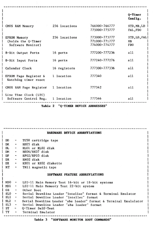
Table 1 "Q-TlMER SPECIFICATIONS"
I
Q-Timer
I
Config.
I
I
CMOS RAM Memory 256 locations 766000-766777 STD,MB,LD
I
775000-775777 FAL,FDO
I
I
EPROM Memory 256 locations 773000-773777 STD,LD,FAL\
(holds the Q-Timer Software Monitor)
8-Bit Output Ports
8-Bit Input Ports
Calendar Clock
EPROM Page Register
&
Watchdog timer reset
CMOS RAM Page Register
Line Time Clock (LTC) Software Control Reg.
771000-771777 774000-774777
16 ports 777200-777236
16 ports 777240-777276
16 registers 777300-777336
1 location 777340
1 location 777342
1 location 777546
Table 2 "Q-TlMER DEVICE ADDRESSES·'
HARDWARE DEVICE ABBREVIATIONS
00 TU58 cartridge tape
OK RK05 disk
OL RL01 or RL02 disk
OM RK06/RK07 disk
OP RP02/RP03 disk
DR RM02 disk
OX RX01 or RX02 diskette
MT TM11 magnetic tape
SOFTWARE FEATURE ABBREVIATIONS
MDO LSI-11 Main Memory Test 16-bit or IS-bit systems
MD1 LSI-11 Main Memeory Test 22-bit system
OB Other Boot
MB FDO
all
all
all
all
all
all
SLO Serial Downline Loader "Intellec" format & Terminal Emulator
SL1 Serial Downline Loader "Intellec" format
SL2 Serial Downline Loader "abs loader" format
&
Terminal EmululatorSL3 Serial Downline Loader "abs loader" format
ST Q-Timer Self-Test
TT Terminal Emulator
Table 3 "SOFTWARE MONITOR BOOT COMMANDS"
[image:8.623.54.553.34.767.2]I
I
I
I
I
I
I
I
I
I
I
I
I
I
I
I
I
I
COPYRIGHT1983 BY
CTICl
I-I
I
loscillator
I I
IA
B CIElI
I
I
I
I
I
I I
I I I
RI4
UI4
I
IHI
I
I
IBYTEI
I
I
I
I
I
I
U20
- I
I
I
Jl
I
I
I
I
I
I
I
UIS
I
I
ILOW
I
IBYTEI
I
I
I
I
I
I
U32
-R8
Esl
D E FI
I
GH
J
I
--_
...
-
---***
E3
***
IKL
MI
UI7
J2
Fl F2
II II
II II
E2
x
+12
INI
E41
pi
I RI
U36
x+12
I-I
I
I
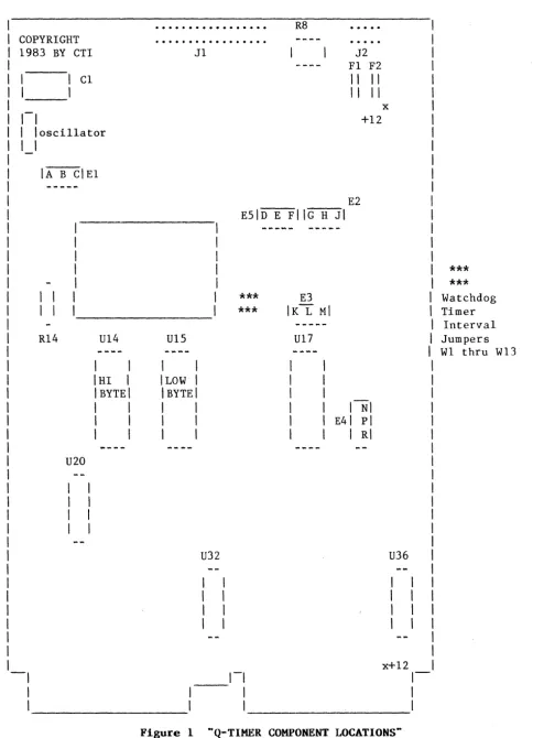
Figure 1 ··Q-TlMER COMPONENT LOCATIONS"
SECTION III -- PAGE 3
I
I
I
***
I
***
I
Watchdog
I
Timer
I
Interval
I
Jumpers
I
WI thru WI3
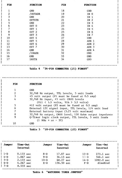
[image:9.624.61.545.56.726.2]PIN FUNCTION PIN FUNCTION
1 GND 18 GND
2 /OUTADR 19 IN 0
3 GND 20 IN 1
4 OUTSTB 21 IN 2
5 GND 22 IN 3
6 OUT 0 23 IN 4
7 OUT 1 24 IN 5
8 OUT 2 25 IN 6
9 OUT 3 26 IN 7
10 OUT 4 27 GND
11 OUT 5 28 ADR 1
12 OUT 6 29 ADR2
13 OUT 7 30 ADR 3
14 GND 31 ADR 4
15 /INADR 32 GND
16 GND 33 GND
17 INSTB 34 GND
Table 4 "34-PIN CONNECTOR (Jl) PINOUT"
PIN FUNCTION
1 GND
2 32,768 Hz output, TTL levels, 5 unit loads
3 +5 volt output (F1 must be fused at 0.5 amp)
4 32,768 Hz input, +5 volt CMOS levels
(ViI
<
1.5 vol ts, Vih>
3.5 vol ts)5 +12 volt output (F2 must be fused at 0.5 amp)
6 External LTC signal input, TTL levels, 1/4 unit load
7 External battery input (5.25 volt maximum)
8 32,768 Hz output, CMOS level, 150 Kohm output impedance
9 Q-Timer logic clock output, TTL levels, 5 unit loads
(1 MHz
+
or - 5%)10 GND
Table 5 "IO-PIN CONNECTOR (J2) PINOUT"
Jumper Time-Out Jumper Time-Out Jumper Time-Out
Interval Interval Interval
1-D 0.133 sec 8-D 17.07 sec 12-D 273.1 sec
4-D 1.067 sec 9-D 34.13 sec 13"D 546.1 sec
5-D 2.133 sec 10-D 68.27 sec 14-D 1092.0 sec
6-D 4.267 sec E-D 136.50 sec F-D disabled
7-D 8.533 sec
~-~~~--~--~--~~~~---~--~---~---Table 6 "WATCHDOG TIMER JUMPERS"
[image:10.617.62.550.49.763.2]Q.
TIMER INSTALLATION
includes: Calendar Clock Software Routine Integration (Step 4)
******************************************************************************
CAUTION: Do not discard any shipping materials until the Q-Timer has been inspected for damage. Notify CODAR Technology and the shipping carrier immediately if any damage is evident. Various time limits, depending on the carrier, may apply concerning the reporting of physical damage.
******************************************************************************
This section provides a 6-step procedure to permit a quick installation of the Q-Timer.
STEP (1) BUS
TERMINATION CHECK
If the Q-Timer is to be used as a bus terminator, the resistor DIP packs U20, U32, and U36 must be installed. If not, they must be removed. If the Q-Timer is to be used as a bus terminator, i t must be placed in the slot in which the bus lines end. In most backplanes this is the slot directly to the right of the CPU. If not, i t can be placed in any vacant board slot (i.e. it does not require bus continuity). The power should always be off when removing or installing boards. See Section III, Figure 1, for the DIP pack locations.
STEP (2)
LINE
TIMECLOCK (LTC) CHECK
Proper configuration of the LTC function is crucial to the correct operation of the LSI-II system. Each processor and system provides various implementations of these functions. The LTC must be provided by either the system or the Q-Timer (in which case it will be a good crystal-controlled LTC). Multiple LTC registers or LTC signals will cause improper system operation. See Section IX, LINE TIME CLOCK, for an explanation of the LTC function and implementation.
STEP (3) ADDRESS CONFLICT CHECK
Before installing the Q-Timer, verify that there will be no address conflicts. To do this you must be in ODT. OnT may be entered on most systems by placing the RUN/HALT switch in the HALT position. When you are in ODT you will receive an "@" prompt on your console terminal. After the prompt you may type the octal memory address you wish to examine followed by a "/". If the memory address is nonexistent, which is the response you are looking for, ODT will type "?"; otherwise it will type the contents of the location.
If you obtain any response from these address checks other than "?" (i.e. OnT shows contents at one of the locations), you must decide whether to disable the function residing at the conflicting address on your present system, or to disable or move the device residing at the conflicting address on the Q-Timer. Changing any of the Q-Timer addresses will necessitate changes in the Q-Timer Software Monitor program (EPROM) as well. Contact CTI
for additional information. Q-Timer Addresses have been chosen which are either used identically for equivalent DEC functions, or are listed as unused in the current DEC Q-BUS address map.
Verify that there is no conflict with the CMOS RAM address space:
@766000/ ? with STD, MB, LD configuration
@766776/ ?
@
@775000/ ? with FAL, FDO configuration
@775777/ ?
@
This procedure checks the first and last locations of CMOS RAM. It is
possible that there are address conflicts between the two limits. If you are
so concerned, you should test every location between.
******************************************************************************
Falcon installations will experience. an address conflict at address
766000 due to the Falcon on-board CMOS RAM. Additionally, if the DEC FALCON
ODT is in use, conflict will also occur at address 773000 (see below). This
can be solved by ordering the Q-Timer with configuration FAL or FDO. See the
Q-TIMER CONFIGURATIONS section of this manual.
******************************************************************************
Verify that there is no conflict with the EPROM address space:
@773000/ ?
@773777/
?
@
@77l000/ ?
@77l777/
?
@
@774000/
?
@774777/
?
with STD, LD, FAL configuration
with MB configuration
with FDO configuration
Again, this procedure checks only the first and last location of the address space.
******************************************************************************
Any existing boot board such as the DEC BDVII will produce a conflict at
address 773000. Additionally, many of the new generation LSI-II system disk
controllers contain on-board boots which are addressed at 773000. The controller boot must be disabled, or the Q-Timer boot address must be moved via the Q-Timer MB configuration. See the Q-TIMER CONFIGURATIONS section of
this manual.
******************************************************************************
Verify that there is no conflict with the 8-bit Output Port address space:
@777200/ ?
@777202/
?
@777236/ ?
@
Verify that there is no conflict with the 8-bit Input Port address space:
@777240/ ?
@777242/
?
@777276/
?
@
Verify that there is no conflict with the Calendar Clock address space:
@777300/ ?
@777302/ ?
@777336/
?
Verify that there is no conflict with the EPROM Page Register, the CMOS RAM Page Register, or the Line Time Clock Software Control Register address space:
@777340/ ?
@777342/ ?
@777546/ ?
@
STEP (4) CALENDAR CLOCK SOFTWARE INTEGRATION
The following contains software routines to integrate the Calendar Clock into RSX-IlM version 3.2, RSX-llM version 4.0, or RT-ll, to allow automatic setting of date and time in your operating system.
******************************************************************************
BEGINNING OF SOFTWARE INTEGRATION******************************************************************************
FOR INTEGRATION into RSX-11K» version 3.2 :
Included in this section are the source and command file listings used to build a program (QTIME.TSK) which will read the calendar clock, and then set
the RSXllM/S system time. Note that this program must be built with the
privileged (/PR) attribute. This program illustrates one technique by which a
program can execute Q-Timer EPROM subroutines. It does not link to the
resident library shown below because, as a task with privileged mapping, it will already be mapped to the I/O page.
We suggest that you put QTIME.TSK into SY:[sysuic], and insert the line:
RUN $QTIME
in your startup command file (SY: [1,2] STARTUP.CMD). This will ensure that
your system loads the proper date and time every time it boots.
QTIME.MAC
Copyright (C) 1983 Codar Technology, Inc.
The following listing is provided for tutorial purposes only.
Note that this program does not check for "busy" status of the EPROM RTIME subroutine.
,
;Note that if you have chosen the MOVE BOOT configuration, change $QROM below from 173000 to 171000 to reflect the new EPROM Software Monitor starting address •
• MCALL EXIT$S
$QROM
=
RTIME
=
$QRPAG
173000 $QROM+062 177340
BEGIN: MOV IIARGS,R5
CLR $QRPAG
JSR PC,RTIME
EMT 376
.WORD EXIT
MOV II$TTNS-14,RO
MOV (R1 )+,(RO)+
MOV (Rl)+,(RO)+
MOV IIMTBL-2,R2
ADD -(R1),R2
ADD (R1)+,R2
MOV (R2),R2
CMP - 2(R1) ,112
BNE 10$
BIT 113,-4(R1)
BNE 10$
INC R2
10$: MOV R2,$TKPS-10
MOV (R1)+ ,( RO)+
MOV (R1)+ ,(RO)+
MOV (Rl )+,(RO)+
MOV (R1)+ ,(RO)+
CLR (RO)+
RTS PC
EXIT: EXIT$S
MTBL: .WORD 32.
.WORD 29.
• WORD 32 •
.WORD 31.
continued on next page
; Starting address of EPROM
; RTIME subroutine entry (in page 0) EPROM page select register
R1
-->
date/time bufferCall RTIME routine in EPROM Switch to system state, with
return to user state at "EXIT:" RO
-->
RSX time locationsYear since 1900 (TTNS-14) Month ($TTNS-12)
R2
-->
days per month tableR2
-->
this month in days per month table R2:=
max days in this month plus oneFebruary? If NE no
Yes -- leap year? If NE no
Yes -- add one for leap day Set RSX days per month parameter
Day ($TTNS-IO) Hour ($TTNS-6) Minute ($TTNS-4)
Second ($TTNS-2) Clear RSX clock ticks Return to user state
January
February (non leap years) March
April
• WORD 32 • May
.WORD 31. June
.WORD 32. July
• WORD 32 • August
.WORD 31- September
.WORD 32. October
.WORD 31- November
• WORD 32 • December
ARGS: .BYTE 1,0 Argument list for "CALL RTIME"
.WORD DATIME
DATIME: • BLKW 9 •
.END BEGIN
The following command file will assemble and link the QTIME task. You
must ensure that the file RSXI1M.STB (or RSX11S.STB, if you are building QTIME to run under an RSX-11S system) is in the directory LB:[sysuic] during the
task-build. This is the file that defines the locations within the RSX
executive that contain the date and time information.
The STB file will have been left in the proper directory by SYSGEN •
.
,
., Copyright( C) 1983 Codar Technology, Inc •
• , The following listing is provided for tutorial purposes only •
.
,
.ENABLE SUBSTITUTION MAC QTIME=QTIME .OPEN BUILD.CMD .ENABLE DATA
QTIME/PR=QTIME,LB:'(SYSUIC)'RSX11M.STB/SS
/
PRI=148 STACK=32 UNITS=O
//
.DISABLE DATA .CLOSE
TKB @BUILD
PIP BUILD.CMD;*/DE,QTIME.OBJ;* PIP QTIME.* /PU
******************************************************************************
END OF RSX-IIM
version3.2 INTEGRATION
BEGINNING OF RSX-IIK
version4.0 INTEGRATION
******************************************************************************
FOR INTEGRATION
into RSX-11K, version4.0 :
The following program will set the date and time for RSX-11M version 4.0 •
• ENABL LC
.TITLE QTIME Set RSXI1M/S V4.0 system date/time
.MCALL STIM$C,EXIT$S
.IDENT /02.02/
The program shown previously for RSX-IIM version 3.2, will actually work under any version of RSX11M or RSX11S.
However, the shorter program shown here can be used specifically under version
4.0,
if the STIM$ directive was included during system generation.$QROM = 173000
RTIME = $QROM+062 $QRPAG = 177340
BEGIN: MOV ilARGS,RS
CLR $QRPAG
JSR PC,RTIME
; Starting address of EPROM
; RTIME subroutine entry (in page 0) EPROM page select register
RS --) argument list Select EPROM page 0
Call RTIME routine in EPROM
MOV 11-1 ,DATIME+S. ,{ICP Use sysgen ticks/second parameter
Set RSX system time STIM$C
EXIT$S
ARGS: .BYTE
.WORD DATIME: .REPT .WORD .ENDR .END DATIME 1,0 DATIME 9. -1 BEGIN
; FORTRAN compatible arg list for CALL RTIME
Buffer for date/time (Init to "default")
******************************************************************************
END OF RSX-llM
version4.0
INTEGRATIONBEGINNING OF RT-ll INTEGRATION
******************************************************************************
FOR INTEGRATION into
RT-ll :
The following program will set the date and time for RT-ll version 4.
Include the command "RUN QTIME" in the file STARTS.COM. Information
regarding older RT-11 versions 2 and 3 is available on request.
Copyright 1983, Codar Technology Inc.
; Note that if you have chosen the MOVE BOOT configuration, change $QROM below ;from 173000 to 171000 to reflect the new EPROM Software Monitor starting
address. .MCALL .GLOBL .EXIT ,.SDTTM JTIME $QROM=173000 RTIME=$QROM+062 $MUL=$QROM+040 $QRPAG=177340
BEGIN: MOV
CLR JSR
IIARGS,RS $QRPAG PC,RTIME
continued on next page
Starting address of EPROM
RTIME subroutine entry (in page 0)
$MUL subroutine
RS --) argument list
Call RTIME subroutine in EPROM
AREA: ARGS: DATIME: JARGS: JHR: JMI: JSE: JTI: RTDTM:
MOV Rl,R5 MOV (R5)+,R2 SUB 1172.,R2
MOV (R5)+,RO. MOV 112000,Rl JSR PC,$MUL BIS R1,R2 MOV (R5)+,RO MOV 1/40,R1
JSR PC,$MUL BIS R1,R2 MOV R2,RTDTM MOV IIJHR,RO MOV (R5)+,(RO)+ MOV (R5)+,(RO)+ MOV (RS)+,(RO)+ CLR (RO)+
MOV IIJARGS,R5 JSR PC,JTIME
.SDTTM IIAREA,IIRTDTM .EXIT
.BLKW 2 .BYTE 1,0 .WORD DATIME
.BLKW 9. .BYTE 5,0 .WORD JHR .WORD JMI • WORD JSE .WORD JT1 .WORD RTDTM+2 .BLKW 1
.BLKW 1 .BLKW 1 .BLKW 1
.BLKW 3
.END BEGIN
Copy pointer
Get year since 1972 in <04:00)
plus month of year in <13:10)
plus day of month in <09:05)
Date is 1st word in RT list
Copy hours for CALL JT1ME Copy minutes
Copy seconds No ticks for now
Convert to RT-style 32-bit integer
******************************************************************************
END OF SOFTWARE INTEGRATION
******************************************************************************
STEP (5) SYSTEM STARTUP
Once the board is in place and the power restored, the system should be started at location 773000. This may happen automatically on power-up if your LSI-II has been so configured, or it may be done from onT by typing "773000G" for STD, LD, and FAL configurations; "771000G" for MB confuration; or "774000G" for FDO configuration.
STEP (6) Q-TIMER SOFTWARE MONITOR OPERATION
The Q-Timer Software Monitor (as delivered) should type the time and date and a prompt
"*"
(if the Q-Timer has previously been configured to auto-boot a device, i t will attempt to do so after printing the date and time). The following section of this manual explains the use of the Software Monitor.Q.
TIMER SOFTWARE MONITOR OPERATION
includes: Boot Commands
Setting the Calendar Clock Time EPROM Page Register Function
Please note that a version of the Q-Timer is available which includes console ODT for FALCON SBC 11/21 systems. With this feature, you can have ODT without tying up the ii/21's on~board memory sockets which otherwise must be used for the DEC Macro-ODT chips. Call CTI for further information.
The EPROM Q-Timer Software Monitor code resides at the standard LS1-11 restart address of 773000 octal with Q-Timer configurations STD, LD, or FAL; at address 771000 octal with Q-Timer configuration MB; or at address 774000 with Q-Timer configuration FDO. If your LSI-11 CPU is configured for automatic boot on power-up, it will automatically go to 773000 and, if the Q-Timer has configuration STD, LD, or FAL, enter the Q-Q-Timer Software Monitor. If the LSI-ll is configured for ODT mode on power-up (i.e. gives you an "@"
prompt), the user should type 773000G or 771000G or 774000G to enter the Software Monitor routine.
If you have set the Q-Timer to auto-boot a designated hardware device (using the
"s"
command as explained later in this section), it will print the date and time as shown below and then attempt to boot the selected device. You can abort this auto bootstrap operation by typing two or three <CTRL C)'s immediately after the date/time message is printed.If you have not set the Q-Timer to auto-boot, the Software Monitor will print to the system console device the day/ date/time and the version number and the processor type, followed by a prompt. For example:
MaN 24-MAY-82 16:28:31 V03.00 11/23
*
If you have the LED/Switch Panel (Test Plug) plugged onto the Q-Timer's 34-pin Connector (I/O Port), the LED's will flash briefly during power-up. The LED's are turned on (i.e. the parallel outputs are set to 1), a read/write check of the Q-Timer's CMOS RAM is performed, and if it succeeds the LED's are then turned off (i.e. the parallel outputs are cleared to 0). If the system hangs with the LED's illuminated a CMOS RAM failure is indicated. Note this is an actual RAM error, and is not caused by loss of battery backup power. Installation of the LED/Switch Panel is not mandatory.
The user may next enter (in response to the Q-Timer's
"*"
prompt) one of eight commands: "E", "T", "J", "S", "B", "1", "2", or "A" followed by a carriage return.EXITING THE Q-TIMER MONITOR: "E"
SETTING THE CALENDAR CLOCK TIME: "T"
Typing "T" yields:
*
DDD DD-MM-YY HH:MMThus the Software Monitor indicates" the exact format for time information entry ("-" is" the prompt). Leading zeros must be typed or the format will not be accepted.
Typing a RETURN without ~nt~ring all time information will cause the current Calendar Clock date'and,time to be printed. To set the time, however, the user should type the form~t indicated: For example, the user may enter:
TUE 05-MAY-82 16:42
Seconds are cleared when you type <RETURN).
NOTE: to handle leap year correctiy, the Q-Timer's date and time must be set (using the Q-Timer ~onitor's "T" command) during the interval between I-JAN 00:00:00.0 and 28-FEB 23:59:59.9 of each leap year.
JUMP COMMAND: .. J"
"J" is the jump command and can be used to transfer control to any location in the EPROM (by PDP-II conv~ntion control must be to a word address, not a byte address). "J" must be followed by the octal jump address which can range from 00000 to 17776. This command allows implementation of customer generated programs, diagnostics, etc.
AUTOMATIC BOOT: -S"
"s"
is the set automatic boot command and is used to specify a device for automatic boot when the Software Monitor is entered (this automatic device specification is stored in the last page of the CMOS memory)."s"
must be followed by one of the same device abbreviations as given for the "B" boot command explained below. The automatic boot is cancelled by typing S<RETURN).If a device is selected for automatic boot, the quebtion arises as to how one may obtain the Q-Timer Software Monitor prompt since every time the Software Monitor is entered, it automatically boots the device. There are two methods: take the current boot device off-line, or type two or three <CTRL C>'s immediately after the Q-Timer prints out the initial date/time (upon power up).
The
"s"
command is very powerful, as it eliminates the need to remove a board and change jumpers or DIP switches to select a different boot device. The selected boot device is protected with a series of check bits in CMOS RAM. If an invalid boot device is detected, control returns automatically to the Q-Timer Monitor. This virtually eliminates the possibility of an attempted boot from an erroneous device due to'corruption of the Q-Timer CMOS RAM.BOOT COMMANDS: "B"
"B" is the boot command,. and must be followed by one of the two or three,:" character abbreviations listed in Table ·3, Section III.
HARDWARE DEVICES
With the 2-character device abbreviations li~t~d in ~he top half of
Table 3, one can add an optional unit designator. As an exampl'e" "B MT2" will
attempt to boot from unit 2 of the system tape drive. The space after the B
is automatically echoed.
SOFTWARE FEATURES
"MDO
for 16 or 18-bit systems; MDI for 22-bit systems."This performs a test of the LSI-II main memory. On unmapped systems,
memory will be tested up to the limit of 56 KB. If the processor has memory
management hardware, it will be employed to t~st memory up to the limit of 248
KB on 18-bit systems, or 4088 KB on 22-bit.systems.
A
message in the format"[mmmmmm] aaaaaa cccccc vvvvvv" (all values are octal)
will be printed for each failing word of memory encountered. "vvvvvv" is the incorrect value actually read from the faulty cell, while "cccccc" is the value which should have been returned. For unmapped systems, "aaaaaa" is the physical address (0 - 157776) of the bad cell. For 18-bit or 22-bit mapped systems, "mmmmmm" is the content of the MMU page address register (0 - 177600) and "aaaaaa" is the virtual address (1 - 17776), mapping the bad cell. The
physical address (P) can be computed as follows:
P
=
(mmmmmm*
100)+
aaaaaa (all values are octal)For example, the line
17400 7746 0 2
indicates that physical location 1740000
+
7746, or 1747746, read back as 2,when it ·should have contained a O.
"OB"
Other Boot provides a means of transferring control to other locations in memory. If you have a Q-Timer with an alternate EPROM address, then "B OB"
will transfer control to 773000 octal. It may also be used in conjunction
with the "A" command to transfer control to anywhere in the lower 56KB of main memory.
"TT"
"B TT" executes a program which allows the local computer to act as a ·'terminal emula tor" (or "v irtual terminal") f or a remo te com puter. In t hi s terminal emulator mode, the local computer is transparent to the local (user)
terminal/console. Thus the local terminal interacts in a direct manner with
the remote computer. In this mode the transparent local computer maintains a
64-character buffer for characters received from the remote computer for transmission to the local terminal. If the buffer is about to overflow~ an X-off character is sent to the remote computer. When the buffer is almost empty an X-on character is sent. If the remote computer responds to these control characters, then it is not necessary to match the baud rates between t:he local terminal and the remote computer. Otherwise the remote computer baud rate must be less than or equal to the local terminal baud rate to prevent data loss from the remote computer.
"SL"
All SL commands and the TT command use the serial line interface at addresses 776500-776507.
"SL1"
"B SL1" executes a program which allows the local computer to accept, as a down-line device, code or data in the INTEL INTELLEC FORMAT from a remote computer. The user is seated at the local computer. This INTELLEC serial format breaks the data into small blocks, each with a start character, a header, data and a checksum. All numbers are encoded in ASCII hex. The
following is an example of the format:
:BBAAAATTDDDD ••• DDCC :BBAAAATTDDDD ••• DDCC
:BBAAAATTDDDD ••• DDCC
BB is the two-character data byte count. AAAA is the four-character destination byte
address.
DD is a data byte.
CC is a one-byte checksum formed by summing the record into an 8-bit register and taking the 2's complement.
TT is the data type. 00 indicates data, 01 indicates end of transmission.
After typing "B SL1" to prepare the local computer for receipt of INTEL format data, the user must next command the remote computer (in whatever manner is dictated by the user Installation) to send the INTEL format data down-line. The last item in the down-line data transfer must be a starting-address record (type 01). This will cause control to immediately transfer to the address given in the address field of that record. If this starting-address record is absent from the down-line data transfer, the program hangs while waiting for more data. If the address is even, control is transferred to that address; if it is odd, exit is made to the Q-Timer monitor.
"SLO"
"B SLOtt implements both the Serial Downline Loader "Intellec" feature and the Terminal Emulator feature.
Typing "B SLO" executes a program which sets up the local computer for receipt of INTEL-format data (acceptor mode), and also implements the Terminal Emulator mode. The :}er is seated at the local computer console. The user can next type the appropriate command (but no RETURN) to instruct the remote computer to begin sending the INTEL-FORMAT data down-line to the transparent local computer (acceptor), and a null character (control-space on some terminals, control-@ on others) and then the RETURN. Following is an example of this for a DEC LSI-II
B SLO
(command line to remote computer><null character)(RETURN)
This command sequence allows the local (user) terminal to command the remote computer to start the down-loading of data to the local transparent
computer. The null character (which is not sent to the remote computer)
indicates to the local transparent computer that one more character will be sent to the remote computer (usually a RETURN) and that the local transparent computer shall then switch into the INTEL-format acceptor mode.
The last item in the down-line data transfer can be a record to transfer control to the starting address of the down-loaded program (this starting address would be encoded in the address field of the record). If this last record/command transfers control back to the Q-Timer Monitor, which it can do by encoding any odd starting address, the Terminal Emulator mode will then not be in effect.
"SL2" or "SL3"
SL2 and SL3 are the implementation in "abs loader" format, of SLO and SL1
respectively. With the abs loader format as created by the RT11 linker, the
data is uncoded. It runs about twice as fast as "Intellec", but requires that
the serial ports at each end be configured for 8-data-bit operation. The abs
loader does not support loading of the Q-Timer CMOS
RAM --
if you wish to doso, you must use the "Intellec" loader SLO or SL1.
"ST"
"B ST" runs the Q-Timer self- test. Selecting "ST" wi th the
"s"
command self-test, is· not generally useful to the Q-Timer user, as it is meant for factory testing."I" or "2" (FALCON only)
For FALCON 11/21 systems, you can set the baud rate on either of the Falcon Serial Line Units (SLU .... s) prior to implementation of the Serial
Downline Loader features. It is recommended that you read the previous
discussion (this section, under BOOT COMMANDS) regarding the SLO/1/2/3 software features.
"I x2<CR)" selects baud rate x for SLU1.
"2 x2<CR)" selects baud rate x for SLU2.
"I <CR)" enables autobaud for SLU1.
Baud rates
o
thru 7 (typed in place of x) are:0 300 baud 3 2400 baud 6 19200 baud
1 600 baud 4 4800 baud 7 38400 baud
2 1200 baud 5 9600 baud
For example, to select 9600 baud before implementing SL2, type;
"2 52<CR>"
"A"
By typing in the "A" command, one can specify an address whicll will be
stored in CMOS RAM. This address will be used in ANY subsequent bootstrap
instead of the normal device address. The syntax of the "A" command is:
A xxxxxx<CR)
A <CR)
where "xxxxxx" is an oc tal address up to 6 digits long. The carriage return is needed only if "xxxxxx" is shorter
than 6 digits.
to clear the alternate address and resume use of the default addresses.
ANY bootstrap which is invoked while the alternate address (set with the
"A" c~and) is in effect will use the alternate address. To return to normal operation, you must clear the alternate address.
No alternate address can be specified for the console terminal, nor for Q-Timer on-board devices.
The "Intellec" format serial line loader (SLO and SL1) does not support the alternate device feature, while the "abs loader" format (SL2 and SL3) does.
Uses of the "A" alternate device address include:
Powering up to any location in the lower 56 KB of main memory, or to any
address in the I/O page (accessa ble via the "OB"boot command, see the previous discussion of "OB" under BOOT 'COMMANDS, this section). For example, to configure the Q-Timer to go to location 1000 for bootstrap:
A 1000<CR) S OB<CR)
sets alternate address to 1000
selects "OB" for Auto-Boot on power up (see SET AUTO-BOOT, this section)
Bootstrapping from a disk or tape controller at other than the standard
addresses (when you have more than one such controller):
A 172420 B MT1
sets an alternate tape controller address
boots unit 1 on the alternate controller (see BOOT COMMANDS, this section)
Using a serial port other than the one at 776500 for "TT" or "SL2/3" (see BOOT COMMANDS, this section):
A 176510 B TT<CR)
sets an alternate Serial Line address implements the Terminal Emulator
EPROM PAGE REGISTER FUNCTION:
The EPROM read-only memory is 4K words long X 16 bits wide, and is fully
byte addressable. Two 2732 EPROM's (each 4K X 8), one for the high byte (U14)
and one for the low byte (U1S), are concatenated to yield the 16 bit word length. The EPROM memory is divided into 16 pages (0 through 15) of 256 words each, and utilizes a 4-bit page offset register. Thus the EPROM uses a
2S6-word block of the I/O page plus 1 2S6-word for the page offset register. The
EPROM memory is supplied from the factory pre-programmed with the Q-Timer
Software Monitor. The EPROM address assignment is 773000 or 771000 or 774000
octal, depending on the Q-Timer conguration as explained in Section II (see also Section III, Table 2).
The EPROM Page Offset Register is used by the Q-Timer Monitor to access
the EPROM memory pages. The EPROM Page Offset Register address assignment is
777340 octal. Only bits 9, 10, 11 and 12 are used to set the page offset
register. Bit 9 is the LSB and bit 12 is the MSB. The EPROM page offset
register is write-only and is cleared to 0 (page 0) on power-up or by a RESET instruction.
The EPROM's are supplied with an opaque label which should not be
removed. This label prevents accidental erasure due to exposure to sources of
strong ultraviolet radiation. The label also contains information regarding
the revision level of the Q-Timer Software Monitor.
CALENDAR CLOCK
******************************************************************************
CAUTION:
THE Q-TIMER CMOS clock oscillator is a high-impedance device; hence care should be exercised when handling the Q-Timer board if the time is to be
preserved while the board is out of the computer. Placing fingers on the
oscillator circuitry may cause it to stop oscillating. While this will not
harm the circuitry, it will result in the loss of time (the oscillator is located in the upper left hand corner of the board directly behind the handle). Setting the board on a conductive surface may short the Ni-Cad battery supply and cause a complete loss of calendar time (as well as the
contents of CMOS RAM). The plastic sheet on the back of the board is designed
to eliminate the possibility of a short.
If the plastic sheet is removed, it must be re-glued with RTV non-corrosive adhesive (i.e. does not contain acetic acid which will corrode the
board). Note that corrosive RTV can usually be identified by a strong
vinegar-like acetic acid smell.
******************************************************************************
The Calendar Clock function occupies 16 consecutive word addresses within the I/O page.
A 32,768 Hz oscillator is used to drive the Calendar Clock (and the LTC circuitry under normal jumper configuration). The output of this on-board oscillator can be monitored on pin 8 of the Q-Timer Auxiliary Connector; the oscillator frequency can be adjusted via capacitor C1 (use a non-metal
screwdriver/device to adjust the capacitor; 1/8 turn corresponds to
approximately 0.1 Hz). The location of these components is shown in Section
III, Figure 1. Note that a 0.1 Hz error in oscillator frequency translates to
a timekeeping error of 0.26 seconds per day, or approximately 7.9 seconds per
month. An accurate frequency counter must be used !
The year, as output by the Q-Timer Software Monitor, is stored in the
Q-Timer CMOS memory and is updated whenever the SET 'TIME COMMAND is used. The
algorithm that maintains the year functions as follows. Whenever the time is
read and the date is in the last half of the year, a flag is set in CMOS RAM. Whenever the time is read and the date is in the first half of the year, the
flag is checked: if it is set the year is incremented and the flag is
cleared. This algorithm will properly maintain the year provided you read the
time at least once in the first half of the year, and at least once in the second half of the year.
Information regarding the Calendar Clock registers is printed in the Codar Technology "Q-TIMER TECHNICAL ADDENDUM", available at no charge from CTI.
WATCHDOG TIMER
The Q-Timer is shipped with the Watchdog Timer disabled. In order to
enable it, the wire-wrap jumper between D and F in Jumper Area E5 must be
removed. Connecting a jumper between D and E in Jumper Area E5 will result in
a time-out interval of 136.5 seconds. Other time-out intervals are available
by installing a jumper from D to the numbered holes around U38. The time-out
intervals that may be obtained are shown in the table below.
When the Watchdog Timer is enabled, location 777340 must be read
periodically to prevent it from timing out. Each read of 777340 or RESET
instruction clears the Watchdog Timer so that the full time-out interval must elapse before the CPU is restarted. If the Watchdog Timer times out, bus line
DCOKH is toggled. This produces the same effect as pressing the RESTART
button on the front panel.
The Q-Timer Software Monitor reads the Q-Timer EPROM Page Select Register periodically to guarantee that the Watchdog Timer does not "bark" during terminal input and other delays.
The Watchdog Timer will be muzzled while the Q-Timer Monitor waits for input from the console, during execution of the Memory Test "MDO/1", Serial Line Loader "SLO/1/2/3", Self-Test "ST", and Terminal Emulator "TT" (see Section V), and during bootstrap operations up to the point at which the secondary boot begins execution.
If the Watchdog Timer is enabled, it is the user's responsibility to ensure that the delay is long enough to permit the system bootstrap to complete, or that the secondary boot contains code to control the Watchdog Timer during the operation.
On FALCON 11/21 systems, the Q-Timer console ODT muzzles the Watchdog Timer during console input if ODT entry was the result of the Q-Timer "E"
command (see Section V), or a BREAK. ODT entries that result from power-up,
HALT execution, or references to non-existent memory by a program are allowed to timeout in order to ensure a system restart after software errors.
JUlDper TiDle-Out Jumper TiDle-Out Jumper Time-Out
Interval Interval Interval
1-D 0.133 sec 8-D 17.07 sec 12-D 273.1 sec
4-D 1.067 sec 9-D 34.13 sec 13-D 546.1 sec
5-D 2.133 sec 10-D 68.27 sec 14-D 1092.0 sec
6-D 4.267 sec E-D 136.50 sec F-D disabled
7-D 8.533 sec
"WATCHDOG TIMER JUMPERS"
CMOS RAM
The CMOS read/write memory is 2048 words long X 16 bits wide, and fully byte addressable. It is divided into 8 pages (0 through 7) of 256 words each, and utilizes a 3-bit page offset register. The memory uses a 256-word block of the I/O page plus 1 word for the Page Offset Register. Thus, at any given time only 256 words of the 2048 total appear in the I/O page. The desired 256 word "page" is selected by writing to the Q-Timer Page Offset Register (location 777342 in the I/O page) using bits 10, 11, and 12. Bit 10 is the LSB and bit 12 the MSB. The Page Select Register is write-only and is cleared to 0 (page 0) on power-up or by a RESET instruction. The Q-Timer CMOS RAM page 7 is reserved for use by the Q-Timer Software Monitor, thus the user can use pages 0 thru 6.
The CMOS RAM may be used as standard program memory. Due to the paging technique, the programmer has access to only 256 words wi thout changing the Page Offset Register. The Page Offset Register needs to be written only once to select a given page, and the selected page will remain selected until either a reset instruction is executed, a power up sequence occurs, or the Page Offset Register is rewritten.
Programs that use the CMOS RAM for data or parameter storage require no unusual programming techniques other than ensuring that the Page Offset Register is properly incremented at the end of a 256 word page (the Page Offset Register does not autoincrement on overflow). Programs, such as device hardware boots, that execute program instructions from CMOS RAM or EPROM require some amount of planning. The program should be optimized to eliminate any unnecessary jumps between 256 word pages. When a new page is selected by writing to the Page Offset Register, the address selected within the page does not change. Thus, if location 140 in page "0" contains an instruction that selects page "5", the next instruction executed will be in location 142 in page "5". This situation is best handled by using reserved locations at the end of a page for transferring control between pages.
******************************************************************************
CAUTION :
As discussed in this Section , Ni-Cad battery backup is provided to make the CMOS RAM and Calendar Clock non-volatile. If the DEC specified power-down sequence is followed, Q-Timer CMOS memory corruption will not occur. If, however, the DEC protocol is not followed there may be adverse consequences. If bus signal BDCOK is not implemented, corruption of the CMOS memory and/or the Calendar Clock may occur during power-up or power-down. If the signal BPOK is not implemented and a CMOS memory location is being written at the time the +5 volt power fails, there is a chance that the single location being accessed will be corrupted. Other locations in the CMOS RAM will be unaffected.
This potential problem may be eliminated by proper implementation of the BPOK signal. The system power supply should assert BPOK at least 4 msec prior to actual power failure. Assertion of BPOK will cause the CPU to trap to the standard power-fail address at 24 octal. The user/programmer is responsible for generating software to insure orderly shutdown as a result of this trap. Specifically, all write operations to either the CMOS RAM or Calendar Clock should be terminated. It is recommended that the customer verify that his LSI-11 chassis does in fact properly implement the DEC power sequencing protocol including both BPOK and BDCOK. Proper implementation is fortunately the rule and not the exception.
******************************************************************************
LINE TIME CLOCK
includes: LTC Jumper Configurations
Experience has shown that system designers do run into problems with the LTC. Many systems generate the 60 HZ LTC directly from the system power supply. You may find it necessary to remove wires from your LSI-II backplane to disable the chassis-generated LTC on your system, if you choose to use the Q-Timer LTC.
******************************************************************************
Note that jumper W4 on the DEC LSI-Il/23 CPU, must be removed to enable BEVENT and to allow the use of an LTC.
******************************************************************************
The Q-Timer LTC (Line Time Clock) circuitry drives the LSI-II bus line BEVNT at a 60 Hz rate. BEVNT is a hardwired LSI-II interrupt which is normally used by RT-II and RSX-II as the operating system clock. The 60 Hz LTC signal is synthesized from the Q-Timer's on-board 32,768 Hz oscillator using a 15/16 pulse-swallowing technique. The same 32,768 Hz oscillator is used to drive the Calendar Clock, thus allowing the use of the LTC and the Calendar Clock in applications requiring the synchronous timing of both functions. The pulse-swallowing synthesis technique resul ts in an extremely small "phase jitter" of about 33us. This is not an inaccuracy or a drift but rather a short term fluctuation which averages to zero. This "phase ji tter" is actually insignificant when compared to fluctuations inherent in 60 Hz clocks derived from the A.C. power line.
The Q-Timer LTC Software Control register responds to the standard DEC address of 777546 octal. The LTC Software Control register (and address) is supported by both RT-II and RSX-Il operating systems. The LTC Software Control register is a single-bit write-only device which is set by writing either "1" or "0" in bit location 6. Writing a "0" disables the LTC interrupts by clamping the BEVNT line to ground. The LTC interrupts are enabled by writing a "I" which releases the clamp on BEVNT. The LTC Software Control register does not actually generate a LTC clock signal; i t only controls (clamps) whatever signal is present on the BEVNT line. Note that the DEC power-up protocol and/or the RESET instruction will clear the LTC Software Control register, thus clamping the BEV ~ line and disabling interruptso
'.
Following are brief descriptions of the STD and LD factory-available "configurations". Alternatively, one can implement one of the following user-installed "al ternatives". The jumper and pin locations are shown in Section III, Figure I.
The STANDARD (STD) configuration and the three "tTC alternatives" (which are not given as available "configurations" from the factory) can be field installed. The LTC DISABLE (LD) configuration requires the use of an EPROM programmer to modify the Q-Timer Address Decoder EPROM to insure a null response by the Q-Timer at the LTC software control address (and thus is given as a factory installed configuration).
STANDARD (STD)
configuration:In the standard configuration, the on-board 32,768 Hz oscillator is used to generate the 60 Hz LTC signal, which drives BEVNT, which in turn is enabled/disabled by the LTC Software Control register.
LTC with External
32,768
Hz alternative:The 60 Hz LTC signal can alternatively be obtained from an external 32,768 Hz oscillator via pin 4 of the Q-Timer Auxiliary Connector. This allows the use of an extremely high accuracy clock if required in the application. This option is jumper selectable (shown later in this section); the external oscillator is not supplied with the Q~Timer.
LTC
with ExternalLTC
alternative:An external LTC signal may be brought in via pin 6 of the Q-timer Auxiliary Connector. This does not have to be 60 Hz and can be any frequency desired (with suitable modifications to the operating system). The signal must be at standard TTL levels, and loading is 1/4 unit load. This option is also jumper selectable (shown later in this section). The functioning of the LTC Software Control register is unchanged.
LTC Clamp
but noLTC
alternative:This alternative disables the 60 Hz LTC signal generated on the Q-Timer, but maintains the LTC Software Control register. The LTC Software Control register will (under software control) clamp/release the LSI-II backplane BEVNT line. This alternative is typically used in systems that generate the 60 Hz LTC signal in the system power supply or by other means. One consequence of this configuration is that the time as maintained by the Calendar Clock chip will not be exactly synchronized with the system time derived from the 60 Hz power line (system power supply).
LTC DISABLE (LD)
configuration:The Q-Timer 60 Hz LTC and t( Q-Timer LTC Software Control register can be completely disconnected from the LSI-II BEVNT line. This is achieved by a two part modification. First the 60 Hz LTC function on the Q-Timer is disabled via jumper configuration (shown later in this section). Next the LTC Software Control register is disabled from responding to its I/O page address. This is accomplished at the facto~y by modifying the Q-Timer Address Decoder EPROM to insure a null response (by the Q-Timer) at the LTC software control address.
******************************************************************************
Proper configuration of the various LTC functions is crucial to the correct operation of the LSI-ll system. Each DEC processor and system provides various combinations of these functions. Multiple LTC registers or LTC signals will cause improper system operation.
******************************************************************************
The following LTC Jumper representation is provided to allow the user to accomplish configuration quickly with minimal description. Each jumper, on the Q-Timer board, consists of 3 pins, and in each case the center pin must be jumpered to one of the pins on either side. See Section III, Figure 1 for jumper locations.
LTC JUMPERS
STANDARD (STD)
configuration: On-board generation of60 Hz,
and LTC Software Control Register ENABLED.El: PINS (A-B) E2: PINS (J-H) E3: PINS (K-L) E4: PINS (N-P)
LTC
with External32,768
Hz
alternative: External 32,768Hz
oscillatorEl: PINS (B-C) E2: PINS (J-H)
via pin 4 of the Q-Timer Auxiliary Connector.
E3: PINS (K-L) E4: PINS (N-P)
LTC
with ExternalLTC
alternative: External signal via pin 6 of the Q-TimerAuxiliary Connector drives the BEVNT line.
El: PINS (A-B) E2: PINS (H-G) E3: PINS (K-L) E4: PINS (N-P)
LTC
Clamp but noLTC
alternative: LTC Software Control Register only, usedto clamp or release BEVNT line.
El: PINS (A- B) E2: don't care E3: PINS (L-M) E4: PINS (N- P)
LTC DISABLE (LD)
configuration: Disable any interaction with BEVNT (Address Decoder EPROM must be changed to· disable BRPLY).El: PINS (A-B) E2: dont care E3: don't care E4: PINS (P-R)
1/0 PORTS & OTHER ITEMS
includes: 34-Pin I/O Port Configuration & Timing lO-Pin Auxiliary Connector Configuration Bus Termination By The Q-Timer
LED/Switch Panel (Test Plug) Use On-Board Rechargeable Batteries
34-PIN I/O PORT CONFIGURATION & TIMING:
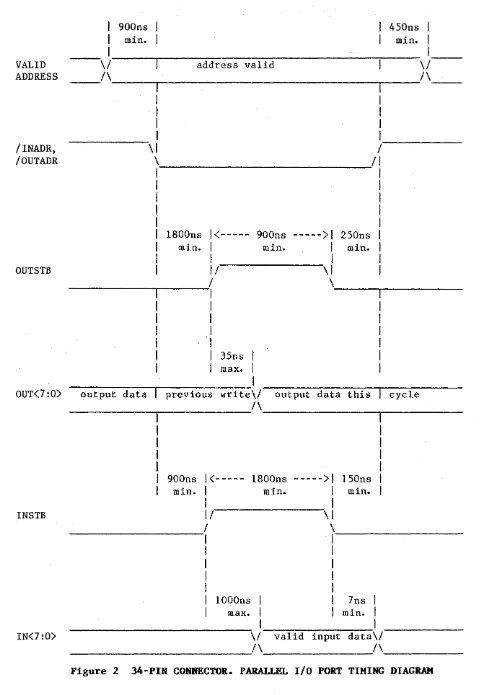
See Section III, Table 4, "34-PIN CONNECTOR (Jl) PINOUT", for the pinout of this port.
The latched 8-bit Parallel Output Port is write-only. Of the data word sent to the port, only bits 0 through 7 are used for data output; the remaining 8 bits are ignored. The Output Port occupies 16 consecutive word addresses within the I/O page. All 16 bus addresses result in a write operation to the same physical port; however, bits 1, 2, 3 and 4 of the bus address are made available on the parallel port connector so that external logic may decode up to 16 different external destination addresses.
The 8-bit Parallel Input Port is read-only and is terminated in 120 ohms at 3.4 volts by SIP resistors RS and R6. The Input Port also responds to 16 bus addresses and can be expanded to 16 input ports using the address bits 1-4 (and external decoding logic). Detailed interface and timing information is provided later in this section.
The Parallel Port connector (Jl) is a standard 34-pin male ribbon connector with "long" latching hardware. A mating connector is not supplied with the Q-Timer; the proper 3M connector number (any equivalent will also work) is # 3414-7034 socket connector, closed end cover with strain relief.
There are two control lines associated with the Input Port, /INADR and INSTB, and 2 lines associated with the Output Port, /OUTADR and OUTSTB. All four control lines are outputs. If one is not attempting to decode port addresses, the 4 address lines (ADR 1-4) and the /INADR and /OUTADR control lines can be disregarded.
All voltage levels are TTL. Output control signals are driven by a 74LS244 octal buffer, and output data lines (OUT 0-7) are driven by a 74LS374 buffer register. Thus, data written to the output port remains latched and stable until the port is written again. Timing information is provided in the following figure.