go.warwick.ac.uk/lib-publications
Original citation:
Komissarova, T. A., Kampert, Erik, Law, J., Jmerik, V. N., Paturi, P., Wang, X., Yoshikawa, A. and Ivanov, S. V. (2018) Electrical properties of surface and interface layers of the N- and In-polar undoped and Mg-doped InN layers grown by PA MBE. Applied Physics Letters, 112 (2). 022104.
Permanent WRAP URL:
http://wrap.warwick.ac.uk/97355
Copyright and reuse:
The Warwick Research Archive Portal (WRAP) makes this work by researchers of the University of Warwick available open access under the following conditions. Copyright © and all moral rights to the version of the paper presented here belong to the individual author(s) and/or other copyright owners. To the extent reasonable and practicable the material made available in WRAP has been checked for eligibility before being made available.
Copies of full items can be used for personal research or study, educational, or not-for profit purposes without prior permission or charge. Provided that the authors, title and full bibliographic details are credited, a hyperlink and/or URL is given for the original metadata page and the content is not changed in any way.
Publisher’s statement:
This article may be downloaded for personal use only. Any other use requires prior permission of the author and AIP Publishing.
Along with the following message:
The following article appeared in Komissarova, T. A., Kampert, Erik, Law, J., Jmerik, V. N., Paturi, P., Wang, X., Yoshikawa, A. and Ivanov, S. V. (2018) Electrical properties of surface and interface layers of the N- and In-polar undoped and Mg-doped InN layers grown by PA MBE. Applied Physics Letters, 112 (2). 022104. and may be found at https://doi.org/10.1063/1.5009794
A note on versions:
The version presented here may differ from the published version or, version of record, if you wish to cite this item you are advised to consult the publisher’s version.
1
Electrical properties of surface and interface layers of the N- and In-polar undoped and
Mg-doped InN layers grown by PA MBE
T.A. Komissarova1*, E. Kampert2, J. Law2, V.N. Jmerik1, P. Paturi3, X. Wang4, A. Yoshikawa5,
and S.V. Ivanov1
1 Ioffe Institute, St. Petersburg 194021, Russia
2 Dresden High Magnetic Field Laboratory, HZDR, Dresden 01328, Germany 3 Wihuri Physical Laboratory, Turku University, Turku 20500, Finland
4 State Key Laboratory of Artificial Microstructure and Mesoscopic Physics, School of Physics,
Peking University, Beijing 100871, China
5 Chiba University, Chiba 263-8522, Japan Abstract
Electrical properties of N-polar undoped and Mg-doped InN layers and In-polar undoped InN
layers grown by plasma-assisted molecular beam epitaxy (PA MBE) were studied. Transport
parameters of the surface and interface layers were determined from the measurements of the
Hall coefficient and resistivity as well as the Shubnikov-de Haas oscillations at magnetic fields
up to 60T. Contributions of the 2D surface, 3D near-interface and 2D interface layers to the total
conductivity of the InN films were defined and discussed as dependent on InN surface polarity,
2
Indium nitride is considered as a compelling material for opto- and microelectronics [1]. One
of the main obstacles towards implementation of the predicted InN applications is its complex
structure including an existence of the surface accumulation layer and the metallic In
nanoparticles occurred in the bulk [1-6]. It is known that two-dimensional (2D) electron
accumulation layers can significantly influence electrical properties of semiconductors [7,8]. The
accumulation layer at the InN surface has been experimentally observed by a high resolution
angle-resolved photoemission spectroscopy (ARPES) [3], a high-resolution electron-energy-loss
spectroscopy (HREELS) [4], an x-ray photoelectron spectroscopy [9], capacitance-voltage
measurements (C-V) [5,10], and a multiple-carrier fitting analysis of the variable-field Hall
measurements [10,11]. It is generally accepted by analogy to conventional semiconductors that
the 2D surface electron accumulation layer masks the properties of the bulk InN epilayer,
shunting its bulk n- and p-type conductivity [1,2,8,12,13]. However, reliable experimental
evidences of the influence of the 2D surface layer on the electrical properties of InN films are
absent. Indeed, ARPES and HREELS methods show just the presence of the InN surface
accumulation layer [3,4]. The C-V technique indicates the difference in electron concentrations
on the surface and in the bulk of InN films [5,9], but it cannot be used for estimation of the
influence of the surface layer on the InN electrical measurements as well as for determination of
a p-type conductivity in the bulk InN, except for showing the presence of acceptor states.
Analysis of results of the variable-field Hall measurements is usually performed without taking
into account the contribution of the metallic indium inclusions [9,10], while they have been
shown to influence strongly the magnetic-field dependences of the Hall coefficient and
resistivity [14, 15]. It was also reported that there could exist a defective layer at the interface
between the InN film and a GaN (AlN) buffer layer due to the large lattice mismatch, which also
may possess different conductivity [12,16]. However, its possible contribution to the total InN
conductivity was not separately studied, and it is usually assumed that the surface and interface
3
[16]. Additionally, it was assumed that the contribution of the 2D surface layer is smaller in case
of In-polar InN films in comparison with N-polar ones [17], however no experimental
comparison of the In- and N-polar InN films has been made to date. Meanwhile, study of the
effects of masking the bulk InN electrical properties by the different conducting channels, as
well as the ways to minimize these parasitic contributions are important in terms of future
electronic and optoelectronic applications of InN and In-rich InGaN.
The goal of this letter is to address all the above assumptions and questions through the
experimental determination of the transport parameters of surface and interface layers in InN
films grown by plasma-assisted molecular beam epitaxy (PA MBE) in different laboratories, and
to reveal their role on the total InN conductivity in dependence on the InN film lattice polarity,
the Mg doping, and the growth conditions. The ways to minimize the influence of these parasitic
conductivity channels are proposed. The electrical properties of the N- and In-polar InN films are
also compared.
Undoped and Mg-doped N-polar and undoped In-polar InN films were grown by PA MBE at
different growth conditions in Ioffe Institute [18], Chiba University [19] and Peking University
[20]. The N-polar InN films were grown at a substrate temperature TS=550°C (samples N1, N2) and 480°C (samples N3-N7). The In-polar InN samples were grown at lower TS= (470-500)°C. The N-polar InN films were grown on c-sapphire substrates with relatively thick PAMBE GaN
buffer layers (100-500 nm). GaN and AlN templates grown by metal-organic chemical vapor
deposition (MOCVD) and capped with thin GaN buffer layers (50-100 nm) were used for growth
of the In-polar InN layers. The Mg concentration in the N-polar InN films was varied in the
range of 1.3×10¹⁷ – 6.0×1018 cm-3 by changing the Mg cell temperature, as estimated by
secondary-ion mass-spectrometry measurements [21,22].
Hall and resistivity measurements were performed in a Hall bar geometry with soldered In
4
Abnormal increasing magnetic-field dependences of the absolute value of the Hall coefficient
(inset in Fig. 1(a)) were measured for all the N-polar InN films. It has been shown earlier that
such a |RH|(B) dependence can serve as an indication of the existence of the metallic In nanoparticles in the InN layers [14]. The values of the electron concentration in the InN
semiconductor matrix nm were determined for the different N-polar InN films (Table 1) from the approximation of the |RH|(B) dependence by using the analysis described in Ref. 14. To obtain the |RH|(B) dependence without contribution of the In nanoparticles (Fig. 1(a)) the approximated curve (dashed line in the inset in Fig. 1(a)) was subtracted from the experimental |RH|(B) dependence.
It has been found that the parasitic conductivity channels have minor influence on the
magnetic-field dependences of the Hall coefficient RH of the N-polar InN films. Indeed, after extracting the influence of the metallic In nanoparticles, which is prevailing in the N-polar InN
[14], the RH(B) dependence becomes almost constant in the temperature range of (4.2-300)K up to high magnetic fields, except for the Shubnikov-de Haas (SdH) oscillations observed at low
temperatures (Fig. 1(a)). Therefore, confirmation of an existence of the additional conducting
channels in the N-polar InN films and, hence, their transport parameters cannot be obtained from
the RH(B) dependence. Instead of that, the parameters of different sublayers of the InN films can be independently determined from the analysis of the SdH oscillations [23]. Three series of the
SdH oscillations identified as the conductivity through the bulk, surface and interface layers
were observed for the N-polar InN films with the Hall mobility µ above 500 cm2/Vs (Fig. 2). Absence of the SdH oscillations for the InN films with the smaller electron mobility is due to
breaking the necessary condition for observation of the SdH oscillations (µB>>1). The dimensionality of the conductive layers was verified by comparison of the SdH oscillations
measured in parallel and normal magnetic field, which in case of a 2D layer should disappear at
5
of the quantized electrons in the sublayers of the InN matrix were determined from the SdH
[image:6.612.112.529.108.260.2]oscillations by using the analysis proposed in Ref. 23 (Table 1).
Fig. 1. Experimental magnetic-field dependences of the absolute value of the Hall coefficient for
the undoped N-polar (a) and In-polar InN layers (b) after subtracting the influence of the metallic
In nanoparticles [14]. The inset in (a) presents the typical measured magnetic-field dependence of
the Hall coefficient for undoped N-polar InN films under study and its approximation (dashed line)
by using the model proposed in Ref. 14.
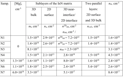
Table 1. Transport parameters of the N-polar undoped and Mg-doped InN films at 4.2 K Samp. [Mg],
cm-3
Sublayers of the InN matrix Two parallel layers: 2D surface and 3D bulk
nm, cm-3
3D bulk 2D surface 3D near-interface/ 2D interface
nb, cm-3 ns, cm-2 n2Dint, cm-2
nint, cm-3 /
ncalc, cm-3
N1
0
1.5×10¹⁸ 2.9×10¹³ n2D
int = 7.2×10¹² 1.5×10¹⁸ 1.6×10¹⁸
N2 1.4×10¹⁸ 2.6×10¹³ n2D
int = 7.2×10¹² 1.4×10¹⁸ 1.4×10¹⁸
N3 8.1×10¹⁷ n
int = 2.3×10¹⁸ 3.1×10¹⁸
N4 1.5×10¹⁸ 2.1×10¹³ 2.8×10¹⁸ 1.5×10¹⁸ 4.3×10¹⁸
N5 1.3×10¹⁷ 1.6×10¹⁸ 1.1×10¹³ 8.0×10¹⁷ 1.6×10¹⁸ 2.4×10¹⁸ N6 1.1×10¹⁸ 1.8×10¹⁷ 2.5×10¹³ 2.4×10¹⁸ 5.4×10¹⁷ 2.6×10¹⁸
[image:6.612.104.529.419.685.2]6
Fig. 2. Shubnikov-de Haas oscillations for the N-polar undoped (#N4 (a) and #N2 (b)) and
Mg-doped InN layers with [Mg] = 1.1×1018 cm-3 (#N6) (c) measured at 4.2K.
The quantized electron concentration of the bulk 3D layer of the studied N-polar undoped
InN films nb was in the range of (0.8-1.5)×1018 cm-3 with the electron mobility (1300-2600) cm2/Vs. The Mg doping reduced n
b to 1.8×1017 cm-3 at [Mg] = 1.1×1018 cm-3.
It has been shown earlier that the values of the electron concentration ns and mobility µs of the 2D surface accumulation layer are in the range of (1-3)×1013 cm-2 (Table 1) and (400-600)
cm2/Vs, respectively, for the studied N-polar InN films [23]. A model of the two parallel
connected layers was used to estimate the influence of the 2D surface layer on the total
conductivity of the InN films [23]. The electron concentrations (ncalc) calculated in the frames of the model, which should be observed for the InN films consisting of the 2D surface and 3D bulk
layers only, are presented in Table 1 as well. It turned out that the ncalc values do not differ much from the transport parameters of the bulk layers themselves in case of the undoped and slightly
Mg-doped InN films, which means the negligible influence of the surface accumulation layer in
these cases. Simultaneously, some of the layers exhibit the nm values measured by Hall effect to be higher than ncal, which indicates the existence of another parasitic conducting channel.
Two types of the interface layers were observed in the N-polar InN films grown at different
conditions. First one is a three-dimensional (3D) near-interface layer (Fig. 2(a,c)) with the
electron concentration of (0.5-2.8)×1018 cm-3 (Table 1). This layer with a thickness of 100-200
nm and the high density of extended defects (1011 cm-2) originates from the large lattice
7
the total conductivity of the InN films due to its high electron concentration and large enough
thickness. Its influence is revealed as the difference between the measured values of the electron
concentration in the InN matrix (nm, Hall) and bulk layer (nb, SdH) (Table 1). Since the existence of the 3D near-interface layer does not affect the magnetic-field dependence of the Hall
coefficient, it is reasonable to assume that the transport electron mobility of this layer is almost
equal to that for the bulk layer of the InN matrix. The 3D near-interface layer of the undoped and
slightly Mg-doped N-polar InN films ([Mg] < 5×1017 cm-3) does not contribute to the SdH
oscillations (Fig. 2a) due to a small distance between the extended defects and the fast electrons
scattering on them [23]. Doping with the higher Mg concentration ([Mg] = 5×10¹⁷ - 5×1018 cm-3)
can lead to appearance of the series of the SdH oscillations at magnetic field normal to the
sample surface, which are presumably related to the conductivity through this layer due to
modification of the near-interface defect structure [23] (Fig. 2(c)). Indeed, it is known that
significant Mg doping can lead to emergence of planar defects (stacking faults) separated from
each other by a small distance (~ 10 nm), which reduces the density of threading dislocations
(TDs) [24]. As a result, electron scattering at the TDs in the 3D near-interface InN layer is
reduced and the SdH oscillations can be observed in the magnetic field normal to the sample
surface.
2D interface layers with the quantized electron concentration of (7-8)×1012 см-2 and the
minimum quantum mobility of (600-800) cm2/Vs were observed in the InN films grown at T S
close to the InN decomposition temperature (above 550ºC). Observation of the series of the SdH
oscillations corresponding to the conductivity through this layer (Fig. 2(b)) indicates the reduced
density of the extended defects at the interface of the high-temperature InN films. Indeed, high
initial TS increases adatoms surface mobility which causes the enlargement of the film grains and corresponding reduction of the extension of the grain boundaries. As a result, reduction of the
8
conductivity of the InN matrix and do not contribute to the magnetic-field dependence of the
Hall coefficient due to its small thickness and the low enough electron concentration.
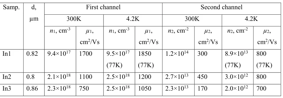
Descending RH(B) dependences corresponding to the conductivity through several channels were observed for the undoped In-polar InN films in contrast to N-polar ones (Fig. 1(b)).
Approximation of the experimental |RH|(B) dependences for the In-polar InN layers (Fig. 1(b)) was performed using a model of two conductive layers connected in parallel [25], using
equations (1)
22 2 2 2 2 1 2 1 1 2 2 2 2 2 1 1 1 2 2 1 1 ) ( 1 1 ) ( / ) ( B B en B B en B B en B en B B B R xy xx xy xx xy H
, (1)
where n1,2 and µ1,2 are the values of electron concentration and mobility, respectively, for the first and second conductive channels. Additionally, contribution of the conductivity of the GaN
template was taken into account. Transport parameters of both conductive channels for selected
undoped In-polar InN layers are presented in Table 2. Since the 2D surface electron
accumulation layer and 2D interface layer should not influence the conductivity of the undoped
InN films, it is reasonable to assume that the first and second channels correspond to the
conductivity of the bulk and 3D near-interface layers of the InN semiconductor matrix,
respectively. It has been found that the electron mobility of the 3D near-interface sublayer is less
than that for the bulk layer in the In-polar InN films (Table 2) in contrast to N-polar ones, which
explains why the 3D near-interface layer influences the magnetic-field dependence of the Hall
coefficient of the In-polar samples. Apparently, such decrease of the electron mobility of the
near-interface layer corresponds to the enhanced density of the near-interface extended defects in
the In-polar InN films. It is not surprising, as the In-polar InN growth should be nucleated at
essentially lower temperatures than the N-polar ones, which results in smaller grain size in the
9
propagate into the bulk. This assumption is confirmed by the fact that no SdH oscillations were
observed for both the near-interface layer and the bulk layer of the In-polar InN samples. The
worse structural quality of the In-polar InN films leads to smaller values of the bulk electron
mobility of (1050-1850 cm2/Vs) in comparison with the N-polar ones (1300-2600 cm2/Vs) at the
[image:10.612.87.567.224.391.2]same electron concentration.
Table 2. Transport parameters of the In-polar undoped InN films. Samp. d,
µm
First channel Second channel
300K 4.2K 300K 4.2K
n1, cm-3 µ1, cm2/Vs
n1, cm-3 µ1, cm2/Vs
n2, cm-2 µ2, cm2/Vs
n2, cm-2 µ2, cm2/Vs In1 0.82 9.4×10¹⁷ 1700 9.5×10¹⁷
(77K)
1850 (77K)
1.2×10¹⁴ 300 8.9×10¹³ (77K)
800 (77K) In2 0.8 2.1×10¹⁸ 1100 2.5×10¹⁸ 1200 2.7×10¹³ 450 3.0×10¹² 800 In3 0.86 2.3×10¹⁸ 750 2.5×10¹⁸ 1050 2.3×10¹³ 170 2.0×10¹² 700
In conclusion, the values of electron concentration and mobility were experimentally
determined for the surface, interface and bulk layers of undoped and Mg-doped N-polar InN
films grown at different temperatures. Two types (2D and 3D) of the interface layers may exist
in the N-polar InN epitaxial layers. It has been shown that 2D surface and interface layers do not
influence noticeably the electrical properties of the InN films with electron concentration and
mobility above 2×1017 cm-3 and 1000 cm2/Vs, respectively. The worse structural and electrical
quality of the In-polar InN layers in comparison with N-polar ones was observed, which is
presumably related to the lower growth nucleation temperatures used for the former. Strong
contribution of the conductivity of the highly defected 3D near-interface layer to the total InN
10
Acknowledgements
T.A.K. and V.N.J. acknowledge the financial support of this work by the Government of the
Russian Federation (contract # 14.W03.31.0011 at the Ioffe Institute). X. Wang acknowledges
the financial supports from the Science Challenge Project (No. TZ2016003-2) and the National
Natural Science Foundation of China (Nos. 61376060 and 61734001).
References
[1] J. Wu, J. Appl. Phys. 106, 011101 (2009)
[2] J.W. Ager III, N. Miller, R.E. Jones, K.M. Yu, J. Wu, W.J. Schaff, and W. Walukiewicz, Phys. Stat. Sol. (b) 245, 873 (2008)
[3] L. Colakerol, T.D. Veal, H.-K. Jeong, L. Plucinski, A. DeMasi, T. Learmonth, P.-A. Glans, S. Wang, Y. Zhang, L.F.J. Piper, P.H. Jefferson, A. Fedorov, T.-C. Chen, T.D. Moustakas, C.F. McConville, K.E. Smith, Phys. Rev. Lett. 97, 237601 (2006)
[4] I. Mahboob, T.D. Veal, C.F. McConville, H. Lu, W.J. Schaff, Phys. Rev. Lett. 92, 036804 (2004)
[5] J.W.L. Yim, R.E. Jones, K.M. Yu, J.W. Ager III, W. Walukiewicz, W.J. Schaff, J. Wu, Phys. Rev. B 76, 041303 (2007)
[6] S.V. Ivanov, T.V. Shubina, T.A. Komissarova, V.N. Jmerik, J. Cryst. Growth 403, 83 (2014)
[7] H.H. Wieder, Appl. Phys. Lett. 25, 206 (1974)
[8] O. Bierwagen, S. Choi, J.S. Speck, Phys. Rev. B. 85, 165205 (2012)
[9] W.M. Linhart, J. Chai, R.J.H. Morris, M.G. Dowsett, C.. McConville, S.M. Durbin, T.D. Veal, Phys. Rev. Lett. 109, 247605 (2012)
[10] P.A. Anderson, C.H. Swartz, D. Carder, R.J. Reeves, S.M. Durbin, S. Chandril, T.H. Myers, Appl. Phys. Lett. 89, 184104 (2006)
[11] C.H. Swartz, R.P. Tomkins, T.H. Myers, H. Lu, and W.J. Schaff, Phys. Stat. Sol. (c) 2, 2250 (2005)
[12] N. Miller, J.W. Ager III, N.M. Smith III, M.A. Mayer, K.M. Yu, E.E. Haller, W. Walukiewicz, W.J. Schaff, C. Gallinat, G. Koblmüller, J.S. Speck, J. Appl. Phys. 107, 113712 (2010)
11
[14] T.A. Komissarova, M.A. Shakhov, V.N. Jmerik, T.V. Shubina, R.V. Parfeniev, S.V. Ivanov, X. Wang and A. Yoshikawa, Appl. Phys. Lett. 95, 012107 (2009)
[15] T.A. Komissarova, M.A. Shakhov, V.N. Jmerik, R.V. Parfeniev, P. Paturi, X. Wang, A. Yoshikawa, S.V. Ivanov, Phys. Rev. B 82, 245204 (2010)
[16] P.D.C. King, T.D. Veal, and C.F. McConville, J. Phys.: Condens. Matter 21, 174201 (2009) [17] L.H. Dmowski, M. Baj, X.Q. Wang, X.T. Zheng, D.Y. Ma, L. Konczewicz, and T. Suski, J.
Appl. Phys. 115, 173704 (2014)
[18] S.V. Ivanov and V.N. Jmerik, Chapter in Nitrides as Seen by the Technology, edited by T. Paskova and B. Monemar, Publisher Research Signpost, Kerala, (2002), p. 369-400.
[19] A. Yoshikawa, X. Wang, Y. Ishitani, A. Uedono, Phys. Stat. Sol. A 207, 1011 (2010)
[20] X. Wang, S. Liu, N. Ma, L. Feng, G. Chen, F. Xu, N. Tang, S. Huang, K.J. Chen, Appl. Phys. Express 5, 015502 (2012)
[21] X. Wang, S.-B. Che, Y. Ishitani, and A. Yoshikawa, Appl. Phys. Lett. 91, 242111 (2007) [22] D. Imai, Y. Ishitani, M. Fujiwara, K. Kusakabe, X. Wang, and A. Yoshikawa, Appl. Phys.
Lett. 98, 181908 (2011)
[23] T.A. Komissarova, V.N. Jmerik, S.V. Ivanov, O. Drachenko, X. Wang, and A. Yoshikawa, Phys. Rev. B 84, 035205 (2011)
[24] Z. Liliental-Weber, M.E. Hawkridge, X. Wang, and A. Yoshikawa, Phys. Stat. Sol. c 7, 2025 (2010)