ISSN Print: 1949-243X
DOI: 10.4236/epe.2018.109025 Sep. 28, 2018 399 Energy and Power Engineering
Performance Analysis of a Boost Converter
with Components Losses
Prince Abdoul Aziz Honadia, Fabé Idrissa Barro
*, Moustapha Sané
Department of Physics, Semiconductors and Solar Energy Laboratory, Faculty of Science and Technique, Cheikh Anta Diop University, Dakar, Senegal
Abstract
A theoretical study of a conventional boost converter is presented. Based on the real behavior of the components, two models of the boost converter are introduced: one dealing only with losses through inductor and capacitor and another taking into account switching losses in addition to resistive ones. From these two models, the detailed analytical expressions of both voltage gain factor and conversion efficiency are established taking into account the losses through parasitic resistances and switching losses. The behavior of the converter is then analyzed for each model by simulation for the voltage gain factor and the conversion efficiency.
Keywords
Boost, Gain Factor, Efficiency, ESR
1. Introduction
Actually, the demand for clean energy sources is actively growing leading to the development of new or alternative energy technologies. These alternative energy technologies are essentially the renewable ones. The most promising renewable energy sources are wind energy, photovoltaic (PV) cells, and fuel cells (FC) [1] [2] [3]. However, renewable energy sources have low output voltage characteris-tics. So, due to this low voltage generation associated to generally high input current requirement, a high step-up DC-DC converter with high efficiency is needed to convert the low DC input to the required voltage, current, and fre-quency. This is particularly true in the case where a microinverter [4]-[9] is pro-vided to each PV module of solar PV systems. Such a microinverter has general-ly two stages; the first stage uses the high step-up DC-DC converter to meet the voltage demand of the second stage and also act as a maximum power point
How to cite this paper: Honadia, P.A.A., Barro, F.I. and Sané, M. (2018) Perfor-mance Analysis of a Boost Converter with Components Losses. Energy and Power Engineering, 10, 399-413.
https://doi.org/10.4236/epe.2018.109025
Received: August 11, 2018 Accepted: September 25, 2018 Published: September 28, 2018
Copyright © 2018 by authors and Scientific Research Publishing Inc. This work is licensed under the Creative Commons Attribution International License (CC BY 4.0).
DOI: 10.4236/epe.2018.109025 400 Energy and Power Engineering
tracker in order to get maximum power from the PV module. The second stage is a DC to AC inverter to meet the load demand.
Many high step-up DC-DC converters have been designed [10] [11] [12] [13] [14] with advantages and disadvantages but all of them derive from the conven-tional boost converter [15]-[20].
The conventional boost converter has many disadvantages like high voltage stress across the switching device and reverse recovery problem of output diode. It is also well know that its performance is limited due to higher on state resis-tance leading to more conduction losses in the switch, losses in the inductor se-ries resistance and the ESR of the output capacitor [21] [22] [23] [24].
These disadvantages are the major limitation of the use of that type of conver-ter. Many works [25] [26] [27] [28] have been carried out dealing with loss mod-els or loss calculation platforms in order to analyze and optimize the power converters before using them into real operation. Some of them use only con-duction loss, missing the switching loss and core loss, which take a large part in the high frequency system losses. Some others took into account switching loss and core loss. A third category used mixed loss model that are able to syntheti-cally and analytisyntheti-cally calculate and analyze the component losses and system losses as functions of voltages, power, switching frequency, operating tempera-ture of the heatsink on the semiconductors and so on. Unfortunately, these stu-dies were not carried out on the basic boost converter but on some, more so-phisticated structure [28] [29]. Even for studies conducted on boost converter, the inductor loss is calculated in number of turn associated to core loss with magnetic effects [30] [31] [32] but not directly versus inductor parasitic resis-tance. Thus, it is important to know exactly how resistive losses and switching losses affect the performance of the converter and what is the contribution of both resistive and switching losses relative to each other and compared to the total losses in the converter. That is the aim of this present study. Based on two loss models of the boost converter, this study will present a detailed mathemati-cal formulation of the voltage gain factor and the conversion efficiency for a conventional boost converter. Simulations are then performed in order to exhi-bit the effects of the different losses but also to quantify these losses compared to the ideal model.
2. Modeling of the Converter and Mathematical Formulation
The studied converter is presented in Figure 1; assuming that all components are ideal and the converter is operating in Continuous Conduction Mode (CCM) [33] as this operating mode is more suited for photovoltaic applications, the ba-sic equations are as follows [34]:
0
0 d
d
in L L
in
V t T
i
v L
V V T t T
t
α
α
< <
= = − < <
(1)
(
)
0 1Vin
V = α
DOI: 10.4236/epe.2018.109025 401 Energy and Power Engineering
with α being the steady state duty cycle and T the switching period.
When taking into account resistive losses through inductor and capacitor, the boost converter can be presented as shown in Figure 2 and the power balance is written as:
0 L C
I r r
P =P P+ +P (3)
PI, PO, PrL, PrC are respectively the input power, the output power, the power
losses through the inductor series resistance rL and the power losses through the
capacitor series resistance rC. Expressing the different terms in Equation (3), see
Appendix, Equation (3) can be rewritten in the form:
(
)
(
)
(
)
2 2
0 0 0 0
0 2 2 2 2
1 1 1
in V V L V C V
V V r r
R R R
α
α
= +α
+α
− − −
∗ ∗ ∗ ∗
(4)
R is the load resistor.
We can then derive the gain factor G as:
(
)
(
)
2(
)
1
1 L C 1
R G
R r r
α
α α α
− =
− + + −
(5)
The conversion efficiency η is defined by:
0 0 rL rC
P
P P P
η=
+ + (6)
Replacing PO, PrL, PrC by their respective expressions, the conversion
[image:3.595.205.541.170.732.2]effi-ciency becomes:
Figure 1. Ideal model of the boost converter.
[image:3.595.212.537.424.710.2]DOI: 10.4236/epe.2018.109025 402 Energy and Power Engineering
(
)
(
)
21 1 1 1 L C r r R η α α α = + − + −
(7)
The model presented above (model 1) did not take into account the switching losses through active components (the Mosfet T and the diode D). The following model of the converter (Figure 3, model 2) do take into account these losses.
The power balance for the converter is:
0 L C
I r r FET D
P P P= + +P +P +P (8)
PFET, PD are respectively the power losses though the switch T and the diode D.
After some mathematical manipulations, we obtain (see Appendix):
(
)
(
)
(
)
(
)
(
)
2 2
0 0 0 0
0 2 2 2
2 2
2
0 0 0
0 0
2 2
1 1 1
1 2
1 1
in L C
DS F F
S
V V V V
V V r r
R R R
r V f C V R V V V
R
R R
α
α α α
α α α ∗ = ∗ + ∗ + − − − + + + + − ∗ −
(9)
fS, rDSon, CO are respectively the transistor switching frequency, on resistance
and output capacitance; rF and VF are the diode dynamic resistance and forward
voltage.
The voltage gain factor G is then deduced as:
(
)
(
)
2(
)
(
)
2 2(
)
2(
)
0
0 1
1
1 1 1 1 1
2 F
L C DS S F
R
G V
R r r r f C R R R
V α
α α α α α α α
− =
− + + − + + − + − + − (10)
For the conversion efficiency, we have:
0
0 rL rC FET D P
P P P P P
η=
+ + + +
(11)
This leads to:
(
)
2(
)
2 00 1 1 1 2 1 1
L DS F C F
S
r r R r V f C R
V
R R
η
α
α
α
α
= + +
+ + + +
− −
(12)
3. Results and Discussions
[image:4.595.219.530.585.707.2]Based on the above mathematical formulation, simulations were performed by
DOI: 10.4236/epe.2018.109025 403 Energy and Power Engineering
varying duty cycle, series resistances, and choosing different transistors and dio-des parameters. This is done for the two models and the effects of the series resis-tances are pointed out, as well as transistor and diode losses.
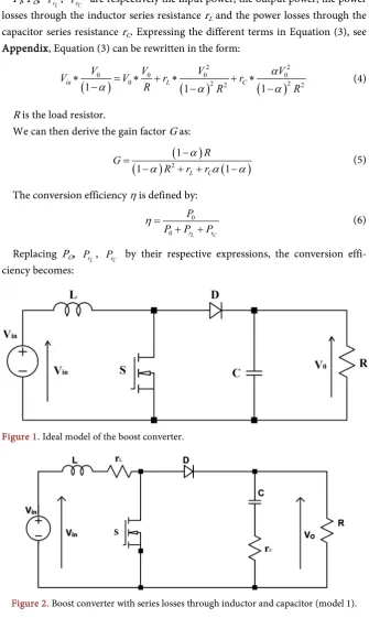
3.1. Voltage Gain Factor
Define We present in Figure 4 the voltage gain factor G versus duty cycle α
for various inductor series resistance rL considering small capacitor series
re-sistance rC (Figure 4(a)) and then larger rC(Figure 4(b)).
(a)
[image:5.595.229.514.203.686.2](b)
DOI: 10.4236/epe.2018.109025 404 Energy and Power Engineering
These figures show that voltage gain factor first increase until a certain du-ty cycle α0value from which it began decreasing. In fact, when the duty cycle
is increasing the losses in the series resistance of the inductor also increase to a threshold from which the losses are so important that the voltage gain factor begin decreasing for duty cycle approaching unity. We can see that this thre-shold depend directly on the series resistance value rL. For low rL the
thre-shold is reached very close to duty cycle equal to unity but for increasing rL
the threshold is reached far from duty cycle equal to unity. This means that the maximum voltage gain factor (corresponding to a duty cycle α0) is shifted
left as rL increases. As losses in the inductor increase, the voltage gain factor
decrease very rapidly. This means that in practical design the value of rL must
be absolutely know otherwise the output voltage could not be guaranteed. Figure 4(a) & Figure 4(b) also show that, regarding the voltage gain factor, there is no significant differences between low rCvalues and high rCvalues.
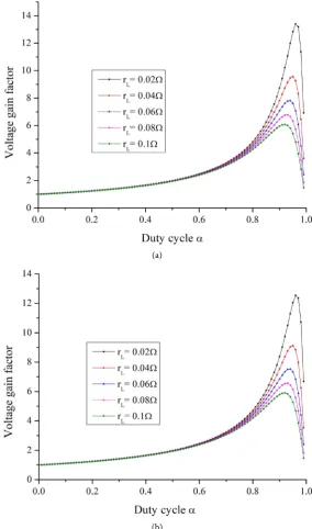
We plotted in Figure 5 the voltage gain factor G versus duty cycle α for various rCconsidering small rL(Figure 5(a)) and larger rL (Figure 5(b)).
These two figures illustrate very well the above situation; for low rLvalue as
for high rLvalue, the effect of the capacitor series resistance is very negligible
on the voltage gain factor. That is, the effect of the capacitor series resistance could be neglected in a first approach in a practical design contrary to the in-ductor series resistance.
Taking into account inductor’s series resistance could lead up to about 54% lower value of the voltage gain factor than that of ideal calculation (rL = 0);
for the case of rC, the gain factor is only up to about 8% lower than ideal
cal-culation (rC= 0). If the output voltage ripple must be kept as low as possible,
then the capacitor resistance should be very low, typically about 10 mΩ (ex-ample for X5R/X7R capacitors). Given that inductor losses also depend on operating frequency the selected inductor must have high quality factor value, typically before quality turning point.
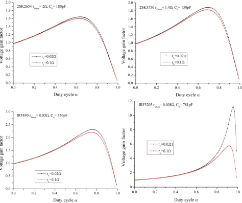
The effect of the output diode is related to its forward voltage VF; this
for-ward voltage has to be as low as possible with also a low dynamic resistance value. This goal can be reached by choosing an appropriate Schottky diode.
For a given operating frequency and a set of inductor, capacitor and diode, the voltage gain factor only depend on the switching transistor characteristics. Figure 6 illustrates the importance of the transistor intrinsic parameters on the voltage gain.
We can see that the major problem comes from the rDSon resistance value for a
given operating frequency: the rDSon value dictate the choice of the switching
tran-sistor when power-rating conditions are satisfied. It can also be noted that the quality of inductor plays a role only when rDSon is low (nearly 50% decrease for a
poor quality inductor); indeed, for higher rDSon values the losses in the transistor
prevail on those from the inductor. When rDSondecrease, the losses through the
DOI: 10.4236/epe.2018.109025 405 Energy and Power Engineering (a) (b)
Figure 5. Voltage gain factor versus duty cycle for various capacitor’s series resistance values. (a) rL = 0.02 Ω; (b) rL = 0.1 Ω.
[image:7.595.60.535.310.707.2]DOI: 10.4236/epe.2018.109025 406 Energy and Power Engineering
3.2. Conversion Efficiency
Figure 6 shows the conversion efficiency profile versus duty cycle for various rL
values considering small rC (Figure 6(a)) and larger rC (Figure 6(b)).
This figure shows that as the duty cycle increases, the conversion decrease and this decrease is very marked for duty cycles close to unity if the series resistance
rLof the inductor is small. When rL is high, the losses in the inductor prevail as
duty cycle increase leading to the observed decrease of the conversion efficiency. It can be noted that the effect of rLis very important for both low and high
capacitor’s series resistance. Taking into account rL could lead to an efficiency
difference up to about 40% compared to unity (ideal conversion efficiency). In Figure 8 the Conversion efficiency profile is presented versus duty cycle for various rC values considering small rL (Figure 8(a)) and larger rL(Figure 8(b)).
As observed before (Figure 5), we can see in Figure 8 that the effect of the se-ries resistance of the capacitor is smaller than that of the sese-ries resistance of the inductor.
With both Figure 7 and Figure 8, we can see that it is recommended to not operate at duty cycles more than 0.8 as series resistances effect are more marked in that area. In fact operating with duty cycle close to unity increase the semi-conductor stress and then decrease markedly the lifetime of the converter.
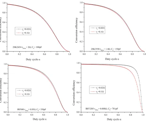
We now present in Figure 9 the conversion efficiency versus duty cycle for different transistors to illustrate transistor characteristics effect on the conver-sion efficiency for a given operating frequency and a set of inductor, capacitor and diode.
Figure 9 shows that rDSon is a very important parameter as noted before in
Figure 6; for high rDSonthe conversion efficiency decrease very markedly as the
duty cycle increase. This decrease can reach 20% or more in the conversion effi-ciency depending on the operating duty cycle. This point out the importance of
(a) (b)
DOI: 10.4236/epe.2018.109025 407 Energy and Power Engineering (a) (b)
Figure 8. Conversion efficiency versus duty cycle for various capacitor’s series resistance values. (a) rL = 0.02 Ω; (b) rL = 0.1 Ω.
[image:9.595.64.538.308.701.2]DOI: 10.4236/epe.2018.109025 408 Energy and Power Engineering
the choice of the switching transistor. The good transistor should then have and
rDSon value as low as possible and in that case inductor losses are the main source
of losses. The capacitance of the transistor is also a limiting factor at high fre-quencies.
4. Conclusions
We have presented in this paper a detailed theoretical study of a conventional boost converter. We have taken into account the real behavior of the passive and active component of the boost converter and we analyzed its voltage gain factor and conversion efficiency. It has been showed that inductor series resistance and transistor rDSon resistance play the most important role leading to a decrease to
up to 50% in the voltage gain factor. We also showed that it is not recommended to use duty cycle close to unity because losses effects are most important there with a markedly decrease of both voltage gain factor and conversion efficiency.
The effect of the capacitor series resistance is negligible for the voltage gain factor (less than 8%) and conversion efficiency; however, the designer must keep in mind that the series resistance of the capacitor directly affect the output ripple voltage and the control loop stability. The last parameter is the switching tran-sistor rDSon that must be as low as possible as the conversion efficiency of the
converter will decrease markedly as duty cycle increase (up to 20%).
Despite its low voltage gain factor, a well-designed conventional boost con-verter can reach the fixed goal with the advantage of a simpler control loop leading to a cost effective and more robust design.
Conflicts of Interest
The authors declare no conflicts of interest regarding the publication of this pa-per.
References
[1] Kesraoui, M., Korichi, N. and Belkadi, A. (2011) Maximum Power Point Tracker of Wind Energy Conversion System. Renew Energy, 36, 2655-2662.
https://doi.org/10.1016/j.renene.2010.04.028
[2] Shuhui, L., Timothy, A.H., Dawen, L. and Fei, H. (2011) Integrating Photovoltaic and Power Converter Characteristics for energy Extraction Study of Solar PV Sys-tems. Renew Energy, 36, 3238-3245.https://doi.org/10.1016/j.renene.2011.02.016
[3] Renewables (2017) Global Status Report, REN21.
[4] Wang, T. and Tang, Y. (2013) A High Step-Up Voltage Gain DC/DC Converter for the Micro-Inverter. IEEE 8th Conference on Industrial Electronics and Applications
(ICIEA), Melbourne, 19-21 June 2013, 1089-1094.
[5] Ternifi, Z.E.T., Petit, P., Bachir, G. and Aillerie, M. (2017) New Topology of Photo-voltaic Microinverter Based on Boost Converter. Energy Procedia, 119, 938-944. https://doi.org/10.1016/j.egypro.2017.07.106
DOI: 10.4236/epe.2018.109025 409 Energy and Power Engineering
Proceedings IPEC, Singapore, 27-29 October 2010, 310-316.
[7] Li, Q. and Wolfs, P. (2008) A Review of the Single Phase Photovoltaic Module Inte-grated Converter Topologies with Three Different DC Link Configurations. IEEE Transactions on Power Electronics,23, 320-1333.
[8] Haibing, H., Qian, Z., Xiang, F., Shen, Z.J. and Batarseh, I. (2011) A Single Stage Micro-Inverter Based on a Three-Port Flyback with Power Decoupling Capability.
Energy Conversion Congress and Exposition (ECCE), Phoenix, 17-22 September 2011, 1411-1416.
[9] Petreuş, D., Daraban, S., Ciocan, I., Patarau, T., Morel, C. and Machmoum, M. (2013) Low Cost Single Stage Micro-Inverter with MPPT for Grid Connected Ap-plications. Solar Energy,92, 241-255. https://doi.org/10.1016/j.solener.2013.03.016
[10] Kazimierczuk, M.K. (2015) Pulse-Width Modulated DC-DC Power Converters. John Wiley and Sons,Hoboken.
[11] Li, W., Lv, X., Deng, Y., Liu, J. and He, X. (2009) A Review of Non-Isolated High Step-Up DC/DC Converters in Renewable Energy Applications. 2009 Twen-ty-Fourth Annual IEEE Applied Power Electronics Conference and Exposition, Washington DC, 15-19 February 2009,364-369.
[12] Wu, G., Ruan, X. and Ye, Z. (2018) Non-Isolated High Step-Up DC-DC Converter Adopting Auxiliary Capacitor and Coupled Inductor. Journal of Modern Power Systems and Clean Energy,6, 384-398.https://doi.org/10.1007/s40565-017-0342-8
[13] Taghvaee, M.H., Radzi, M.A.M., Moosavain, S.M., Hizam, H. and Marhaban, M.H. (2013) A Current and Future Study on Non-Isolated DC-DC Converters for Pho-tovoltaic Applications. Renewable and Sustainable Energy Reviews, 17, 216-227. https://doi.org/10.1016/j.rser.2012.09.023
[14] Wu, K.C. (1997) Pulse Width Modulated DC-DC Converters. Springer,Berlin.
https://doi.org/10.1007/978-1-4615-6021-0
[15] Ayop, R. and Tan, C.W. (2018) Design of Boost Converter Based on Maximum Power Point Resistance for Photovoltaic Applications. Solar Energy, 160, 322-335. https://doi.org/10.1016/j.solener.2017.12.016
[16] Winder, S. (2017) Power Supplies for LED Driving. 2nd Edition, Newnes, Oxford and Boston.
[17] Dash, S.S. and Nayak, B. (2015) Control Analysis and Experimental Verification of a Practical DC-DC Boost Converter. Journal of Electrical Systems and Information Technology, 2, 378-390. https://doi.org/10.1016/j.jesit.2015.08.001
[18] Abusorrah, A., Al-Hindawi, M.M., Al-Turki, Y., Mandal, K., Giaouris, D., Banerjee, S., Voutetakis, S. and Papadopoulou, S. (2013) Stability of a Boost Converter Fed from Photovoltaic Source. Solar Energy, 98, 458-471.
https://doi.org/10.1016/j.solener.2013.09.001
[19] Wu, K. (2016) Power Converters with Digital Filter Feedback Control. Academic Press, Cambridge.
[20] Sadek, U., Sarjaš, A., Svečko, R. and Chowdhury, A. (2015) FPGA-Based Control of a DC-DC Boost Converter. IFAC-PapersOnLine, 48, 22-27.
https://doi.org/10.1016/j.ifacol.2015.08.102
[21] Erickson, R.W. and Maksimovic, D. (2004) Fundamentals of Power Electronics. 2nd Edition, Kluwer Academic Publishers, New York.
Oc-DOI: 10.4236/epe.2018.109025 410 Energy and Power Engineering tober 2012, 5744-5749.
[23] Rajesh, R. and Mabel, M.C. (2015) A Comprehensive Review of Photovoltaic Sys-tems. Renewable and Sustainable Energy Reviews, 51, 231-248.
https://doi.org/10.1016/j.rser.2015.06.006
[24] Mahela, O.P. and Shaik, A.G. (2017) Comprehensive Overview of Grid Interfaced Solar Photovoltaic Systems. Renewable and Sustainable Energy Reviews, 68, 316-332. https://doi.org/10.1016/j.rser.2016.09.096
[25] Bae, J.Y., Kim, Y., Lee, D.H., Kwon, S.D., Kim P.S. and Han, D.H. (2004) A Study on the Loss Model and Characteristic Comparison of Three Level Converter and Full-Bridge Converter through the Conduction Loss Analysis of Power Devices.
IEEE IECON, 3, 2314-2320.
[26] Hayashi, Y., Takao, K., Shimizu, T. and Ohashi, H. (2007) Power Loss Design Plat-form for High Output Power Density Converters. European Conference on Power Electronics and Applications, Aalborg, 2-5 September 2007, 1-10.
[27] Deng, S., Mao, H., Wu, T., Xiao, S. and Batarseh, I. (2004) Power Losses Estimation Platform for Power Converters. IEEE 19th Annual Applied Power Electronics Con-ference and Exposition, Anaheim, 22-26 February 2004, Vol. 3, 1784-1789.
[28] Wang, Y., Haan, S. and Ferreira, J.A. (2008) Methods for Experimental Assessment of Component Losses to Validate the Converter Loss Model. IEEE 13th Interna-tional Power Electronics and Motion Control Conference, Poznan, 1-3 September 2008, 187-194.
[29] Beldjajev, V., Roasto, I. and Zakis, J. (2013) Impact of Component Losses on the Ef-ficiency of a New Quasi-Z-Source-Based Dual Active Bridge. Doctoral Conference on Computing, Electrical and Industrial Systems, Costa de Caparica, 15-17 April 2013, 485-492.
[30] Gadalla, B.S.A., Schaltz, E., Siwakoti, Y.P. and Blaabjerg, F. (2017) Analysis of Loss Distribution of Conventional Boost, Z-Source and Y-Source Converters for Wide Power and Voltage Range. Transaction on Environment and Electrical Engineering, 2, 1-9. https://doi.org/10.22149/teee.v2i1.68
[31] Tsai, M.-Y., Liang, T.-J. and Lin, Y.-M. (2017) Loss Analysis and Optimized Design of DC-DC Converter for Battery Module. IEEE 3rd International Future Energy Electronics Conference and ECCE Asia, Kaohsiung, 3-7 Jun 2017, 692-697.
[32] Hinov, N., Arnaudov, D., Valchev, V. and Vuchev, S. (2017) Comparative Loss Analysis of Boost and Synchronous Boost DC-DC Converters. International Scien-tific Conference Electronics, Sozopol, 13-15 September 2017, 1-4.
[33] Durán, E., Andújar, J.M., Segura, F. and Barragán, A.J. (2011) A High-Flexibility DC Load for Fuel Cell and Solar Arrays Power Sources Based on DC-DC Conver-ters. Applied Energy, 88, 1690-1702. https://doi.org/10.1016/j.apenergy.2010.11.002
DOI: 10.4236/epe.2018.109025 411 Energy and Power Engineering
Appendix
When the switch S is on, we have:
d dL
L in i
v V L
t
= =
(A.1) Integrating this equation give rise to the current flowing through the coil L:
( )
IL Lm V
i t I t
L
= + (A.2)
with ILm being the minimum of iL.
When T is off, the voltage across L can be written as:
0 ddL
L I i
v V V L
t
= − =
(A.3) This above equation give rise to iL in the form:
( )
I 0L LM V V
i t I t
L −
= +
(A.4) with now ILM being the maximum of iL.
ILMand ILmare reached respectively at the switching on and off of S and are
related by:
(
)
0 I Lm LM V V
I I T
L τ
−
= + −
I LM Lm V
I I
Lτ
= +
with T being the switching period, α the duty cycle and τ α= T. Combining
these two equations, we obtain the output voltage V0 as (2):
(
)
0 1Vin
V
α =
−
The power dissipated through rL is: 2
L
r L ISR
P = +r I
(A.5) with
(
1 0)
ISR I I
I I
α = =
−
(A.6)
The power dissipated through rCis given by: 2
C rms
r C C
P =r +I (A.7)
with 2 0 1 d rms T C C
I i t
T =
∫
(A.8) and 0 0 0 C II t T
i
I I T t T
α α − < <
= − < <
DOI: 10.4236/epe.2018.109025 412 Energy and Power Engineering
replacing iC by the above equation leads to:
(
)
0 1
rms
C
I I
α
α
=
−
(A.10)
The output current IO is:
0 0 V I
R =
The power dissipated in the switch can be written as:
1 2
DS
FET r SW
P =P + P
(A.11)
where PrDS is the losses through the drain-source on resistance rDS and PSW the
switching losses. We then have:
2
DS rms
r DS S
P =r ∗I
(A.12) where 2 0 1 d rms T S S
I i t
T
=
∫
(A.13)and
(
1 0)
00 I C
I
I t T
i
T t T α α
α
= < <
−
=
< <
(A.14)
Inserting Equation (A.14) into Equation (A.13) we obtain:
(
)
0 1
rms
S
I I
α
α
=
−
(A.15)
The switching losses are given by:
2 0 2
0 0
SW S SM S
P = f C V = f C V (A.16)
The total losses in the switch S are then:
(
)
02 2 0 02 1 2 1
FET DS S
P r I α f C V
α
= +
− (A.17)
The power losses in the diode D is
F F
D R V
P =P +P
(A.18) where
2
F rms
R F D
P =R ∗I
and 2 0 1 d rms T D D
I i t
T
=
∫
DOI: 10.4236/epe.2018.109025 413 Energy and Power Engineering
(
0)
0 0
1 D
I
t T
I
i I T t T
α
α α
< <
= = < <
−
These above equations lead to:
(
10)
rmsD I
I
α
= −
and then:
(
)
2 0 1
F
R F I
P R
α
=
− (A.19)
The last term in the power losses in the diode D is:
0
F
V F D F
P =V I =V I